EP4131335A1 - Procédé de fabrication de tranche liée et tranche liée - Google Patents
Procédé de fabrication de tranche liée et tranche liée Download PDFInfo
- Publication number
- EP4131335A1 EP4131335A1 EP21775084.3A EP21775084A EP4131335A1 EP 4131335 A1 EP4131335 A1 EP 4131335A1 EP 21775084 A EP21775084 A EP 21775084A EP 4131335 A1 EP4131335 A1 EP 4131335A1
- Authority
- EP
- European Patent Office
- Prior art keywords
- wafer
- bonded
- bonding
- layer
- compound semiconductor
- Prior art date
- Legal status (The legal status is an assumption and is not a legal conclusion. Google has not performed a legal analysis and makes no representation as to the accuracy of the status listed.)
- Pending
Links
Images




Classifications
-
- H—ELECTRICITY
- H10—SEMICONDUCTOR DEVICES; ELECTRIC SOLID-STATE DEVICES NOT OTHERWISE PROVIDED FOR
- H10H—INORGANIC LIGHT-EMITTING SEMICONDUCTOR DEVICES HAVING POTENTIAL BARRIERS
- H10H20/00—Individual inorganic light-emitting semiconductor devices having potential barriers, e.g. light-emitting diodes [LED]
- H10H20/01—Manufacture or treatment
- H10H20/011—Manufacture or treatment of bodies, e.g. forming semiconductor layers
- H10H20/018—Bonding of wafers
-
- H—ELECTRICITY
- H10—SEMICONDUCTOR DEVICES; ELECTRIC SOLID-STATE DEVICES NOT OTHERWISE PROVIDED FOR
- H10P—GENERIC PROCESSES OR APPARATUS FOR THE MANUFACTURE OR TREATMENT OF DEVICES COVERED BY CLASS H10
- H10P10/00—Bonding of wafers, substrates or parts of devices
- H10P10/12—Bonding of semiconductor wafers or semiconductor substrates to semiconductor wafers or semiconductor substrates
- H10P10/128—Bonding of semiconductor wafers or semiconductor substrates to semiconductor wafers or semiconductor substrates by direct semiconductor to semiconductor bonding
-
- H—ELECTRICITY
- H10—SEMICONDUCTOR DEVICES; ELECTRIC SOLID-STATE DEVICES NOT OTHERWISE PROVIDED FOR
- H10H—INORGANIC LIGHT-EMITTING SEMICONDUCTOR DEVICES HAVING POTENTIAL BARRIERS
- H10H20/00—Individual inorganic light-emitting semiconductor devices having potential barriers, e.g. light-emitting diodes [LED]
- H10H20/01—Manufacture or treatment
- H10H20/011—Manufacture or treatment of bodies, e.g. forming semiconductor layers
- H10H20/013—Manufacture or treatment of bodies, e.g. forming semiconductor layers having light-emitting regions comprising only Group III-V materials
-
- H—ELECTRICITY
- H10—SEMICONDUCTOR DEVICES; ELECTRIC SOLID-STATE DEVICES NOT OTHERWISE PROVIDED FOR
- H10H—INORGANIC LIGHT-EMITTING SEMICONDUCTOR DEVICES HAVING POTENTIAL BARRIERS
- H10H20/00—Individual inorganic light-emitting semiconductor devices having potential barriers, e.g. light-emitting diodes [LED]
- H10H20/80—Constructional details
- H10H20/81—Bodies
- H10H20/822—Materials of the light-emitting regions
- H10H20/824—Materials of the light-emitting regions comprising only Group III-V materials, e.g. GaP
-
- H—ELECTRICITY
- H10—SEMICONDUCTOR DEVICES; ELECTRIC SOLID-STATE DEVICES NOT OTHERWISE PROVIDED FOR
- H10P—GENERIC PROCESSES OR APPARATUS FOR THE MANUFACTURE OR TREATMENT OF DEVICES COVERED BY CLASS H10
- H10P10/00—Bonding of wafers, substrates or parts of devices
- H10P10/12—Bonding of semiconductor wafers or semiconductor substrates to semiconductor wafers or semiconductor substrates
-
- H—ELECTRICITY
- H10—SEMICONDUCTOR DEVICES; ELECTRIC SOLID-STATE DEVICES NOT OTHERWISE PROVIDED FOR
- H10P—GENERIC PROCESSES OR APPARATUS FOR THE MANUFACTURE OR TREATMENT OF DEVICES COVERED BY CLASS H10
- H10P90/00—Preparation of wafers not covered by a single main group of this subclass, e.g. wafer reinforcement
-
- H—ELECTRICITY
- H10—SEMICONDUCTOR DEVICES; ELECTRIC SOLID-STATE DEVICES NOT OTHERWISE PROVIDED FOR
- H10P—GENERIC PROCESSES OR APPARATUS FOR THE MANUFACTURE OR TREATMENT OF DEVICES COVERED BY CLASS H10
- H10P50/00—Etching of wafers, substrates or parts of devices
- H10P50/60—Wet etching
- H10P50/64—Wet etching of semiconductor materials
- H10P50/642—Chemical etching
- H10P50/646—Chemical etching of Group III-V materials
Definitions
- the present invention relates to a method for manufacturing a bonded wafer, and a bonded wafer.
- Epitaxial wafers for various compound semiconductor devices have been manufactured by using GaAs substrates and InP substrates.
- the maximum diameters of GaAs substrates are 6 inches (150 mm), and InP substrates are 4 inches (100 mm) substrates.
- a groove designed for small diameter is cut in a wafer with large diameter to prepare a template, and a compound semiconductor wafer is placed thereon and subjected to the subsequent process.
- This method can be performed easily at low cost, but has a problem that the template and the wafer are not physically in close contact.
- a photolithography process requires a step of heating a wafer with a hot plate before and after exposing a resist to light.
- this brings about a problem that the thermal resistance between the template and the wafer is increased, making the photolithography conditions unstable.
- Patent Document 1 discloses a method in which a template wafer and an EPW are bonded using a polyimide material for tentative immobilization, and then processed.
- This method is an excellent method in terms of attachment to the template.
- the delamination from the template is necessary.
- a residue remains on the delaminated surface, so that the removal step needs to be performed.
- oxygen plasma ashing needs to be performed. This results in a problem that the surface of the compound wafer is oxidized in the removal step.
- compound EPWs have hetero-epitaxial structures.
- the growth is carried out such that lattice constants are made substantially the same by adjusting the growth temperature.
- warp is caused due to difference in coefficient of thermal expansion.
- internal stress is generated in the compound semiconductor epitaxial layer. This internal stress continuously changes with temperatures.
- a to-be-bonded member has a smaller coefficient of thermal expansion than an EPW substrate
- tensile stress is applied to the EPW substrate. The larger the tensile stress, the more likely it is that the substrate is cracked.
- a template substrate is made of silicon, the coefficient of thermal expansion is lower than that of a compound semiconductor. Hence, the compound semiconductor EPW bonded by heating receives tensile stress after the temperature is lowered to room temperature.
- Patent Document 1 6213977 B2
- An object of the present invention is to provide a method for manufacturing a bonded wafer by which crack formation in an epitaxial layer is suppressed when a substrate allowing device processing is prepared by bonding the compound semiconductor epitaxial wafer with small diameter or small size onto a to-be-bonded wafer.
- the present invention provides a method for manufacturing a bonded wafer, the method comprising bonding a to-be-bonded wafer and a compound semiconductor wafer that includes a compound semiconductor epitaxially grown on a growth substrate, wherein
- a substrate allowing device processing is prepared by bonding a compound semiconductor wafer with small diameter or small size onto a to-be-bonded wafer, a growth substrate is removed after the bonding, so that the epitaxial layer in the resulting bonded wafer has less crack formation.
- the bonding of the to-be-bonded wafer and the compound semiconductor wafer is preferably performed by any method of direct bonding with no interposition therebetween, metal bonding with a metal, and bonding with a resin or polymer interposed therebetween.
- Such bonding methods can facilitate the bonding to some extent, and the bonded product can be directly utilized as a final device element.
- the metal preferably comprises at least one or more of Au, Ag, Al, In, and Ga.
- the resin or polymer preferably comprises benzocyclobutene, polyimide, or glass with TEOS.
- the bonding is preferably performed such that a center of the compound semiconductor wafer and a center of the to-be-bonded wafer are arranged to deviate from each other by 5 mm or less.
- the compound semiconductor wafer from which the growth substrate has been removed may have a total thickness of 15 um or less.
- the to-be-bonded wafer comprises silicon, sapphire, or quartz preferably.
- the present invention provides a bonded wafer comprising:
- the epitaxial layer in the bonded wafer has less crack formation.
- the inventive method for manufacturing a bonded wafer makes it possible to manufacture a bonded wafer in a thin film form whose epitaxial layer has crack formation suppressed by removing a growth substrate after the compound semiconductor epitaxial wafer with small diameter or small size is bonded onto a to-be-bonded wafer when a substrate allowing device processing is prepared. Moreover, the inventive bonded wafer has an epitaxial layer with successfully suppressed crack formation.
- the present inventors have earnestly studied the above problems and consequently found the following method for manufacturing a bonded wafer by bonding a to-be-bonded wafer and a compound semiconductor wafer including a compound semiconductor epitaxially grown on a growth substrate.
- the bonding surface area of the to-be-bonded wafer is larger than the bonding surface area of the compound semiconductor wafer.
- the growth substrate is removed after the to-be-bonded wafer is bonded to the bonding surface of the compound semiconductor wafer, which is the compound semiconductor side, where the epitaxial growth takes place.
- a bonded wafer including a compound semiconductor wafer and a to-be-bonded wafer bonded thereto and having an area larger than the bonding surface area of the compound semiconductor wafer.
- the compound semiconductor wafer has a total thickness of 15 ⁇ m or less.
- This bonded wafer is a bonded wafer with satisfactorily suppressed crack formation in the epitaxial layer. This finding has led to the completion of the present invention.
- a bonded wafer according to the present invention and a method for manufacturing a bonded wafer which can be employed for the inventive bonded wafer. Nevertheless, the present invention is not limited thereto.
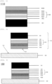
- a compound semiconductor wafer (EPW) 110 is prepared which includes: a growth substrate (starting substrate) 101, for example, made of GaAs having a thickness of 550 um and a diameter of 6 inches; a light-emitting-diode-functional layer 103 made of AlGaInP; and an etch stop (ES) layer 102 made of InGaP or InAlP or AlGaInP having a thickness of 0.1 um.
- the light-emitting-diode-functional layer 103 and the etch stop (ES) layer 102 are formed by an MOVPE method, for example.
- the etch stop (ES) layer 102 is formed between the growth substrate and the light-emitting-diode-functional layer.
- the AlGaInP-based light-emitting-diode-functional layer 103 can sequentially include from the starting substrate 101 side: for example, a p-type Al 1-y In y P layer 1031 (0.4 ⁇ y ⁇ 0.5) having a thickness of 1 um and a carrier concentration of approximately 1 ⁇ 10 17 /cm 3 ; an (Al 1-x Ga x ) 1-y In y P layer (active layer) 1032 (0.45 ⁇ x ⁇ 1, 0.4 ⁇ y ⁇ 0.5) having a thickness of 0.6 ⁇ m; and an n-type Al 1-y In y P layer 1033 (0.4 ⁇ y ⁇ 0.5) having a thickness of 1 ⁇ m and a carrier concentration of approximately 1 ⁇ 10 17 /cm 3 .
- the thicknesses of the p-type Al 1-y In y P layer 1031, the active layer 1032, and the n-type Al 1-y In y P layer 1033 are not limited to the exemplified numerical values.
- the carrier concentrations can be set within a range up to approximately 3 ⁇ 10 18 /cm 3 depending on the required function. Further, the carrier concentration profiles are not limited to uniform distribution, either. Furthermore, the exemplified carrier concentrations are average carrier concentrations, and it is a matter of course that these concentrations conceptually include partially low carrier concentration state (e.g., approximately 0.7 ⁇ 10 15 /cm 3 ).
- a window layer may be provided as necessary.
- GaP is suitably selected for the AlGaInP-based light-emitting-diode-functional layer structure.
- the window layer 1035 made of GaP and having a thickness of approximately 10 um may be stacked.
- a reduction layer 1034 made of Ga 1-y In y P layer (0 ⁇ y ⁇ 1) may be provided to reduce band discontinuity amount.
- AlGaInP-based light-emitting-diode-functional layer is exemplified here, any function and structure can be selected, as long as the lattice constant of the material matches that of the GaAs substrate.
- AlGaInP-based semiconductor laser it is also possible to apply InGaP-based hetero bipolar transistor and field-effect transistor, InGaP/GaAs-based solar cell, GaAsP-based photodiode, etc.
- InGaAs-based hetero bipolar transistor and field-effect transistor InGaAs-based light-emitting device (semiconductor laser and light-emitting diode), InGaAs(P)-based photodiode, etc.
- the functional layer including a window layer has a total thickness of 15 um or less; in other words, the compound semiconductor wafer from which the growth substrate is removed, which will be described later, has a total thickness of 15 um or less.
- designing the total thickness to be 7 ⁇ m or less can further suppress crack formation.
- the lower limit value of the total thickness is not particularly limited, but is preferably 0.5 ⁇ m or more.
- the to-be-bonded wafer 120 is prepared as shown in FIG. 2 .
- the to-be-bonded wafer is preferably a wafer having sufficient flatness, for example, silicon, sapphire, or quartz. This can reduce the cost of the to-be-bonded wafer.
- a silicon wafer having a diameter of 8 inches is usable.
- an area of a bonding surface of the to-be-bonded wafer is larger than an area of a bonding surface of the compound semiconductor wafer.
- a circular wafer is exemplified, but the wafer shape is not particularly limited and may be, for example, rectangular, square, etc.
- both of the EPW 110 and the to-be-bonded wafer 120 are subjected to wet surface treatment with an alkaline solvent.
- the wafers may be immersed in a 5 wt% NaOH aqueous solution for 10 minutes, then rinsed, and dried in air.
- both of the EPW 110 and the to-be-bonded wafer 120 are introduced into a bonding apparatus such that an epitaxial surface 131 of the EPW 110 and a polished surface 121 of the to-be-bonded wafer 120 face and are superposed on each other.
- the wafers are bonded at 200°C under vacuum atmosphere to prepare a bonded substrate 150.
- the bonding is preferably performed such that the center of the compound semiconductor wafer and the center of the to-be-bonded wafer are arranged to deviate from each other by 5 mm or less. In this manner, crack formation can be suppressed.
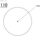
- a central point 1101 of the EPW 110 shown in FIG. 4 is preferably arranged at such a position that the deviation from a central point 1201 of the to-be-bonded wafer 120 shown in FIG. 5 is minimized to 5 mm or less.
- the centers are obvious.
- the central point 1101 is re-defined as the center of mass. (e.g., in the case of a rectangular shape, the central point 1101 is defined as an intersection where diagonals intersect.)
- the to-be-bonded wafer is bonded to a side, where the compound semiconductors are epitaxially grown, as the bonding surface of the compound semiconductor wafer.
- the pressure during the bonding can be 5 N/cm 2 or more and 400 N/cm 2 or less based on the pressure applied to the EPW 110.
- the applied pressure thus exemplified is not limited to this range.
- the applied pressure is not limited to the exemplified range. It is a matter of course that a pressure higher than this range is also applicable.
- the bonding progresses when the alkali-treated surfaces contact.
- the bonding is possible even at a pressure lower than the exemplified pressure.
- a buffer material is placed between the two wafers, and the buffer material is pulled out under vacuum to bring the wafers into contact with each other. In this case, no pressure is applied. At this process stage, the pressure application is not always necessary.
- the starting substrate 101 is removed from the bonded substrate 150 by wet etching.
- the wet etching is performed with a liquid mixture of ammonia and hydrogen peroxide water (APM). Since the APM liquid has etching selectivity with respect to the ES layer 102, only GaAs is etched, and the etching is stopped at the ES layer 102.
- APM liquid has etching selectivity with respect to the ES layer 102, only GaAs is etched, and the etching is stopped at the ES layer 102.
- a starting substrate-removed wafer 160 can be obtained from the bonded substrate 150 from which only the GaAs substrate serving as the growth substrate is removed.
- the substrate-removed surface is covered with a silicon wafer 170 having a diameter of 6 inches.
- a silicon wafer is selected as the cover material, an inexpensive material reliably having flatness is preferable and is not limited to silicon.
- the silicon wafer 170 is not limited to silicon having a diameter of 6 inches, and a wafer having a diameter of 8 inches or more can also be selected in accordance with the diameter of the to-be-bonded member 120. Selecting either wafer makes no difference in result.
- the bonded wafer having the cover wafer placed thereon is subjected to compression bonding under vacuum atmosphere and heated at a temperature of 500°C or less.
- the compression bonding is performed at a pressure of 5 N/cm 2 or more and 400 N/cm 2 or less.
- the heating time can be approximately 5 minutes. The longer the heating time, the higher the strength. In this step, the heating may be performed at a higher temperature than this disclosure, as long as it is possible to keep sufficient strength to prevent delamination of the epitaxial layer in the subsequent heating step.
- the silicon wafer 170 is removed and the starting substrate-removed wafer 160 is introduced into a heating furnace.
- the atmosphere of the heating furnace is selected in accordance with the material of the surface from which the substrate has been removed. Since the InGaP layer is exposed in the first embodiment, the heating is performed under a P atmosphere (1 ⁇ 10 5 atm). When an InP substrate is used, an As-based material, such as GaAs, is exposed; in this case, the heating is performed under an As atmosphere (1 ⁇ 10 5 atm).
- the heating is performed at a temperature of 600 to 800°C.
- the heating temperature is preferably higher because high strength is obtained within shorter time by higher temperature. To achieve this, high group-V pressure is required. Thus, adjustment may be made appropriately depending on the system to be manufactured, design, etc.
- a compound semiconductor wafer (EPW) 210 is prepared which includes: a growth substrate (starting substrate) 201, for example, made of GaAs having a thickness of 550 ⁇ m and a diameter of 6 inches; a light-emitting-diode-functional layer 203 made of AlGaInP; and an etch stop (ES) layer 202 made of InGaP or InAlP or AlGaInP having a thickness of 0.1 um.
- the light-emitting-diode-functional layer 203 and the etch stop (ES) layer 202 are formed by an MOVPE method, for example.
- the etch stop (ES) layer 202 is formed between the starting substrate and the functional layer.
- the AlGaInP-based light-emitting-diode-functional layer 203 can sequentially include from the starting substrate 201 side: for example, a p-type Al 1-y In y P layer 2031 (0.4 ⁇ y ⁇ 0.5) having a thickness of 1 um and a carrier concentration of approximately 1 ⁇ 10 17 /cm 3 ; an (Al 1-x Ga x ) 1-y In y P layer (active layer) 2032 (0.45 ⁇ x ⁇ 1, 0.4 ⁇ y ⁇ 0.5) having a thickness of 0.6 um; and an n-type Al 1-y In y P layer 2033 (0.4 ⁇ y ⁇ 0.5) having a thickness of 1 um and a carrier concentration of approximately 1 ⁇ 10 17 /cm 3 .
- the thicknesses of the p-type Al 1-y In y P layer 2031, the active layer 2032, and the n-type Al 1-y In y P layer 2033 are not limited to the exemplified numerical values.
- the carrier concentrations can be set within a range up to approximately 3 ⁇ 10 18 /cm 3 , depending on the required function. Further, the carrier concentration profiles are not limited to uniform distribution, either. Furthermore, the exemplified carrier concentrations are average carrier concentrations, and it is a matter of course that these concentrations conceptually include partially low carrier concentration state (e.g., approximately 0.7 ⁇ 10 15 /cm 3 ).
- a window layer may be provided as necessary.
- GaP is suitably selected for the AlGaInP-based light-emitting-diode-functional layer structure.
- the window layer 2035 made of GaP and having a thickness of approximately 10 um may be stacked.
- a reduction layer 2034 made of Ga 1-y In y P layer (0 ⁇ y ⁇ 1) may be provided to reduce band discontinuity amount.
- AlGaInP-based light-emitting-diode-functional layer is exemplified here, any function and structure can be selected, as long as the lattice constant of the material matches that of the GaAs substrate.
- AlGaInP-based semiconductor laser it is also possible to apply InGaP-based hetero bipolar transistor and field-effect transistor, InGaP/GaAs-based solar cell, GaAsP-based photodiode, etc.
- InGaAs-based hetero bipolar transistor and field-effect transistor InGaAs-based light-emitting device (semiconductor laser and light-emitting diode), InGaAs(P)-based photodiode, etc.
- the functional layer including a window layer has a total thickness of 15 ⁇ m or less; in other words, the compound semiconductor wafer from which the growth substrate is removed, which will be described later, has a total thickness of 15 ⁇ m or less.
- the lower limit value of the total thickness is not particularly limited, but is preferably 0.5 um or more.
- the to-be-bonded wafer is preferably a wafer having sufficient flatness, for example, silicon, sapphire, or quartz. These can reduce the cost of the to-be-bonded wafer.
- the to-be-bonded wafer 220 a silicon wafer having a diameter of 8 inches is usable.
- an area of a bonding surface of the to-be-bonded wafer is larger than an area of a bonding surface of the compound semiconductor wafer.
- a circular wafer is exemplified, but the wafer shape is not particularly limited and may be, for example, rectangular, square, etc.
- the to-be-bonded wafer and the compound semiconductor wafer are preferably bonded by metal bonding with a metal.
- the bonding can be performed relatively easily, and the bonded resultant can be directly used as a final device element.
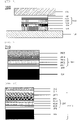
- metal films are vapor-deposited on both of the EPW 210 and the to-be-bonded wafer 220.
- EPW 210 for example, a 0.1- ⁇ m Ti layer 211 and a 1-pm Au layer 212 can be provided as vapor-deposited films.
- silicon wafer for example, a 0.1-pm Ti layer 221 and a 1- ⁇ m Au layer 222 can be provided as vapor-deposited films.
- these structures and film thicknesses are exemplified, it is a matter of course that any material can be selected if required for the bonding.
- the metal in the metal bonding preferably includes at least one or more of Au, Ag, Al, In, and Ga. These can suppress yield reduction due to bonding failure in the bonding.
- the material of the uppermost layer desirably contains at least one or more of Au, Ag, Al, In, and Ga, and the film thickness is desirably 0.3 um or more.
- the film thickness may be large without limitation. However, the large thickness brings similar effect in terms of yield.
- the upper limit of the film thickness is determined from economical viewpoint. From economical viewpoint, 3 ⁇ m or less is desirable.
- both of the EPW 210 and the to-be-bonded wafer 220 are introduced into a bonding apparatus such that the Au layer 212 of the EPW and the Au layer 222 of the to-be-bonded wafer face and are superposed on each other.
- the wafers are bonded to prepare a bonded substrate 250.
- the bonding is preferably performed such that the center of the compound semiconductor wafer and the center of the to-be-bonded wafer are arranged to deviate from each other by 5 mm or less. In this manner, crack formation can be further suppressed.
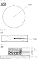
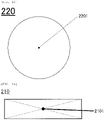
- a central point 2101 of the EPW 210 shown in FIG. 14 is preferably arranged at such a position that the deviation from a central point 2201 of the to-be-bonded wafer 220 shown in FIG. 15 is minimized to 5 mm or less.
- the centers are obvious.
- the central point 2101 is re-defined as the center of mass. (e.g., in the case of a rectangular shape, the central point 2101 is defined as an intersection where diagonals intersect.)
- the to-be-bonded wafer is bonded to a side, where the compound semiconductors are epitaxially grown, as the bonding surface of the compound semiconductor wafer.
- the pressure during the bonding can be 5 N/cm 2 or more and 400 N/cm 2 or less based on the pressure applied to the compound EPW with small diameter. Simultaneously, a heat at a temperature of 400°C or less can also be applied.
- the applied pressure thus exemplified is not limited to this range.
- the bonding is performed under a condition where the EPW 210 with small diameter withstands the applied pressure (e.g., the substrate thickness is increased)
- the applied pressure is not limited to the exemplified range, and a pressure higher than this range is also applicable.
- the pressure application and heating are simultaneously performed here.
- the pressure application and the heat treatment may be performed separately such that the application is performed solely, followed by heating, for example.
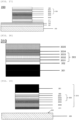
- the starting substrate 201 is removed from the bonded substrate 250 shown in FIG. 13 by wet etching.
- the wet etching is performed with a liquid mixture of ammonia and hydrogen peroxide water (APM). Since the APM liquid has etching selectivity with respect to the ES layer 202, only GaAs is etched, and the etching is stopped at the ES layer 202.
- APM liquid has etching selectivity with respect to the ES layer 202, only GaAs is etched, and the etching is stopped at the ES layer 202.
- a starting substrate-removed wafer 260 can be obtained from the bonded substrate 250 from which only the GaAs substrate serving as the growth substrate is removed.
- a compound semiconductor epitaxial wafer (EPW) 310 is prepared which includes: a growth substrate (starting substrate) 301, for example, made of GaAs having a thickness of 550 um and a diameter of 6 inches; a light-emitting-diode-functional layer 303 made of AlGaInP; and an etch stop (ES) layer 302 made of InGaP or InAlP or AlGaInP having a thickness of 0.1 ⁇ m between the starting substrate and the functional layer.
- start substrate starting substrate
- ES etch stop
- the AlGaInP-based light-emitting-diode-functional layer 303 can sequentially include from the starting substrate 301 side: for example, a p-type Al 1-y In y P layer 3031 (0.4 ⁇ y ⁇ 0.5) having a thickness of 1 um and a carrier concentration of approximately 1 ⁇ 10 17 /cm 3 ; an (Al 1-x Ga x ) 1-y In y P layer (active layer) 3032 (0.45 ⁇ x ⁇ 1, 0.4 ⁇ y ⁇ 0.5) having a thickness of 0.6 ⁇ m; and an n-type Al 1-y In y P layer 3033 (0.4 ⁇ y ⁇ 0.5) having a thickness of 1 um and a carrier concentration of approximately 1 ⁇ 10 17 /cm 3 .
- a basic structure is exemplified, and the thicknesses of the p-type layer 3031, the active layer 3032, and the n-type layer 3033 are not limited to the exemplified numerical values.
- the carrier concentrations can be set within a range up to approximately 3 ⁇ 10 18 /cm 3 depending on the required function. Further, the carrier concentration profiles are not limited to uniform distribution, either. Furthermore, the exemplified carrier concentrations are average carrier concentrations, and it is a matter of course that these concentrations conceptually include partially low carrier concentration state (e.g., approximately 0.7 ⁇ 10 15 /cm 3 ).
- a window layer may be provided as necessary.
- GaP is suitably selected for the AlGaInP-based light-emitting-diode-functional layer structure.
- the window layer 3035 made of GaP and having a thickness of 10 ⁇ m is stacked.
- a reduction layer 3034 made of Ga 1-y In y P layer (0 ⁇ y ⁇ 1) may be provided to reduce band discontinuity amount.
- AlGaInP-based light-emitting-diode-functional layer is exemplified here, any function and structure can be selected, as long as the lattice constant of the material matches that of the GaAs substrate.
- AlGaInP-based semiconductor laser it is also possible to apply InGaP-based hetero bipolar transistor and field-effect transistor, InGaP/GaAs-based solar cell, GaAsP-based photodiode, etc.
- InGaAs-based hetero bipolar transistor and field-effect transistor InGaAs-based light-emitting device (semiconductor laser and light-emitting diode), InGaAs(P)-based photodiode, etc.
- the functional layer including a window layer has a total thickness of 15 ⁇ m or less; in other words, the compound semiconductor wafer from which the growth substrate is removed, which will be described later, has a total thickness of 15 ⁇ m or less.
- the lower limit value of the total thickness is not particularly limited, but is preferably 0.5 ⁇ m or more.
- a to-be-bonded wafer 320 is prepared as shown in FIG. 19 .
- the to-be-bonded wafer is preferably a wafer having sufficient flatness, for example, silicon, sapphire, or quartz. This can reduce the cost of the to-be-bonded wafer.
- a silicon wafer having a diameter of 8 inches is usable.
- an area of a bonding surface of the to-be-bonded wafer is larger than an area of a bonding surface of the compound semiconductor wafer.
- a circular wafer is exemplified, but the wafer shape is not particularly limited and may be, for example, rectangular, square, etc.
- the to-be-bonded wafer and the compound semiconductor wafer are preferably bonded by bonding with a resin or polymer interposed therebetween.
- the bonding can be performed relatively easily, and the bonded resultant can be directly used as a final device element.
- the resin or polymer is preferably benzocyclobutene, polyimide, or glass with TEOS. In these ways, yield reduction due to bonding failure in the bonding can be further suppressed.
- the EPW 310 is spin-coated with benzocyclobutene (BCB).
- BCB benzocyclobutene
- the viscosity and the number of spinnings are adjusted to form a BCB film 311 having a thickness of approximately 3 ⁇ m, for example.
- exemplified is a case of forming the BCB film 311 on only the EPW 310.
- the BCB film 311 may be formed on both of the EPW 310 and the to-be-bonded wafer 320, or may be formed on only the to-be-bonded wafer 320. In these cases, similar effects are obtained.
- the film thickness can be changed within approximately 0.5 to 20 um by adjusting the viscosity. Nevertheless, since increasing the BCB film thickness increases the thermal resistance, the BCB thickness is preferably approximately 0.5 to 20 ⁇ m at most. Further, forming a thick BCB film causes cost increase. From these viewpoints, the film thickness is appropriately 12 ⁇ m or less, but may exceed this range.
- spin-coating with BCB is exemplified here, spin-coating with polyimide (PI) instead of BCB may be performed. Meanwhile, similar effects are obtained by spin-coating with TEOS after a porous silicon film or another porous film is formed on the EPW 310, or on the to-be-bonded wafer 320, or on both of the EPW 310 and the to-be-bonded wafer 320.
- PI polyimide
- both of the EPW 310 and the to-be-bonded wafer 320 are introduced into a bonding apparatus such that the BCB layer 311 of the EPW and a surface 321 of the to-be-bonded wafer face and are superposed on each other.
- the wafers are bonded to prepare a bonded substrate 350.
- the bonding is preferably performed such that the center of the compound semiconductor wafer and the center of the to-be-bonded wafer are arranged to deviate from each other by 5 mm or less. In this manner, crack formation can be suppressed.
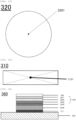
- a central point 3101 of the EPW 310 shown in FIG. 21 is preferably arranged at such a position that the deviation from a central point 3201 of the to-be-bonded wafer 320 shown in FIG. 22 is minimized to 5 mm or less.
- the centers are obvious.
- the central point 3101 is re-defined as the center of mass. (e.g., in the case of a rectangular shape, the central point 3101 is defined as an intersection where diagonals intersect.)
- the to-be-bonded wafer is bonded to a side, where the compound semiconductors are epitaxially grown, as the bonding surface of the compound semiconductor wafer.
- the pressure during the bonding can be 5 N/cm 2 or more and 400 N/cm 2 or less based on the pressure applied to the compound EPW with small diameter.
- the applied pressure thus exemplified is not limited to this range.
- the bonding is performed under a condition where the EPW 310 with small diameter withstands the applied pressure (e.g., the substrate thickness is increased), is not limited to the exemplified range, a pressure higher than this range is also applicable.
- the pressure application and heating may be performed simultaneously here. Similar effects are obtained even when the pressure application and the heat treatment are performed separately such that the application is performed solely, followed by heating, for example.
- the starting substrate 301 is removed from the bonded substrate 350 by wet etching.
- the wet etching is performed with a liquid mixture of ammonia and hydrogen peroxide water (APM). Since the APM liquid has etching selectivity with respect to the ES layer 302, only GaAs is etched, and the etching is stopped at the ES layer 302. Hence, as shown in FIG. 24 , a starting substrate-removed wafer 360 can be obtained from the bonded substrate 350 from which only the GaAs substrate serving as the growth substrate is removed.
- APM ammonia and hydrogen peroxide water
- the epitaxial wafers (EPWs) 110 were prepared each of which included: the growth substrate (starting substrate) 101 made of GaAs having a thickness of 550 um and a diameter of 6 inches (150 mm); the AlGaInP-based light-emitting-diode-functional layer 103; and the etch stop (ES) layer 102 made of InGaP having a thickness of 0.1 um and located between the starting substrate and the light-emitting-diode-functional layer.
- the growth substrate (starting substrate) 101 made of GaAs having a thickness of 550 um and a diameter of 6 inches (150 mm
- the AlGaInP-based light-emitting-diode-functional layer 103 the etch stop (ES) layer 102 made of InGaP having a thickness of 0.1 um and located between the starting substrate and the light-emitting-diode-functional layer.
- the AlGaInP-based light-emitting-diode-functional layer 103 sequentially included from the starting substrate 101 side: the p-type Al 1-y In y P layer 1031 (0.4 ⁇ y ⁇ 0.5) having a thickness of 1 ⁇ m and a carrier concentration of approximately 1 ⁇ 10 17 /cm 3 ; the (Al 1-x Ga x ) 1-y In y P layer (active layer) 1032 (0.45 ⁇ x ⁇ 1, 0.4 ⁇ y ⁇ 0.5) having a thickness of 0.6 um; and the n-type Al 1-y In y P layer 1033 (0.4 ⁇ y ⁇ 0.5) having a thickness of 1 ⁇ m and a carrier concentration of approximately 1 ⁇ 10 17 /cm 3 .
- the window layer 1035 made of GaP having a thickness of 10 um was stacked. Further, between the window layer 1035 and the functional layer 103, the reduction layer 1034 made of Ga 1-y In y P layer (0 ⁇ y ⁇ 1) was provided to reduce band discontinuity amount.
- silicon wafers having a diameter of 8 inches (200 mm) were used as the to-be-bonded wafers 120.
- Each pair of the EPW 110 and the to-be-bonded wafer 120 were introduced into a bonding apparatus such that the epitaxial surface 131 of the EPW 110 and the polished surface 121 of the to-be-bonded wafer 120 faced and were superposed on each other.
- the wafers were bonded at 200°C under vacuum atmosphere to prepare the bonded substrate 150.
- the paired wafers were bonded such that the deviation of the central point 1101 of the EPW 110 from the central point 1201 of the to-be-bonded wafer 120 was altered from 1 to 9 mm by 1 mm among the pairs. Moreover, the pressure during the bonding was 50 N/cm 2 . These are shown in Table 1.
- Example 1 Example 2
- Example 3 Growth substrate GaAs GaAs GaAs Thickness [ ⁇ m] of growth substrate 550 550 550 Diameter [inch] of growth substrate 6 6 6 Etch stop layer InGaP InGaP InGaP Thickness [um] of etch stop layer 0.1 0.1 0.1 Functional layer AlGaInP-based AlGaInP-based AlGaInP-based Thickness [um] of p-type Al 1-y In y P layer 1 1 1 Thickness [ ⁇ m] of active layer 0.6 0.6 0.6 Thickness [um] of n-type Al 1-y In y P layer 1 1 1 1 Window layer GaP GaP GaP Thickness [ ⁇ m] of window layer 10 10 10 Reduction layer Ga 1-y In y P Ga 1-y In y P Ga 1-y In y P Ga 1-y In y P To-be-bonded wafer silicon silicon silicon Diameter [inch] of to-be-bonded wafer 8 8 8 Bonding method direct bonding metal bonding resin or polymer
- the starting substrate 101 was removed from the bonded substrate 150 by wet etching.
- the wet etching was performed with a liquid mixture of ammonia and hydrogen peroxide water (APM). Since the APM liquid has etching selectivity with respect to the ES layer 102, only GaAs is etched, and the etching is stopped at the ES layer 102. Thus, only the GaAs substrate serving as the growth substrate was removed from the bonded substrate 150, and the starting substrate-removed wafer 160 was obtained.
- APM ammonia and hydrogen peroxide water
- the surface from which the starting substrate was removed was covered with the silicon wafer 170 having a diameter of 6 inches.
- the bonded wafer having the cover wafer placed thereon was subjected to compression bonding under vacuum atmosphere and heated at a temperature of 200°C.
- the pressure was 50 N/cm 2 .
- the heating time was 5 minutes in this Example.
- the silicon wafer 170 was removed, and the starting substrate-removed wafer 160 was introduced into a heating furnace.
- the InGaP layer was exposed.
- the heating was performed under a P atmosphere (1 ⁇ 10 5 atm). The heating was performed at a temperature of 700°C for approximately 30 minutes.
- FIG. 25 shows the number of cracks in relation to the deviation of the central point 1101 of the EPW 110 from the central point 1201 of the to-be-bonded wafer 120 in the bonded wafers prepared as above.
- the epitaxial wafers (EPWs) 210 were prepared each of which included: the growth substrate (starting substrate) 201 made of GaAs having a thickness of 550 ⁇ m and a diameter of 6 inches; the AlGaInP-based light-emitting-diode-functional layer 203; and the etch stop (ES) layer 202 made of InGaP having a thickness of 0.1 ⁇ m and located between the starting substrate and the light-emitting-diode-functional layer.
- starting substrate the growth substrate
- ES etch stop
- the AlGaInP-based light-emitting-diode-functional layer 203 sequentially included from the starting substrate 201 side: the p-type Al 1-y In y P layer 2031 (0.4 ⁇ y ⁇ 0.5) having a thickness of 1 ⁇ m and a carrier concentration of approximately 1 ⁇ 10 17 /cm 3 ; the (Al 1-x Ga x ) 1-y In y P layer (active layer) 2032 (0.45 ⁇ x ⁇ 1, 0.4 ⁇ y ⁇ 0.5) having a thickness of 0.6 ⁇ m; and the n-type Al 1-y In y P layer 2033 (0.4 ⁇ y ⁇ 0.5) having a thickness of 1 um and a carrier concentration of approximately 1 ⁇ 10 17 /cm 3 .
- the window layer 2035 made of GaP having a thickness of 10 ⁇ m was stacked. Further, between the window layer 2035 and the functional layer 203, the reduction layer 2034 made of Ga 1-y In y P layer (0 ⁇ y ⁇ 1) was provided to reduce band discontinuity amount.
- silicon wafers having a diameter of 8 inches were used as the to-be-bonded wafers 220.
- metal films were vapor-deposited on each EPW 210 and to-be-bonded wafer 220.
- the EPW 210 the 0.1- ⁇ m Ti layer 211 and the 1-pm Au layer 212 were provided as vapor-deposited films.
- the silicon wafer the 0.1-pm Ti layer 221 and the I- ⁇ m Au layer 222 were provided as vapor-deposited films.
- Each pair of the EPW 210 and the to-be-bonded wafer 220 were introduced into a bonding apparatus such that the Au layer 212 of the EPW and the Au layer 222 of the to-be-bonded wafer faced and were superposed on each other.
- the wafers were bonded to prepare the bonded substrate 250.
- the paired wafers were bonded such that the deviation of the central point 2101 of the EPW 210 from the central point 2201 of the to-be-bonded wafer 220 was altered from 1 to 9 mm by 1 mm among the pairs.
- the pressure during the bonding was 50 N/cm 2 .
- heating was also performed at 350°C. These are also shown in Table 1.
- the starting substrate 201 was removed from the bonded substrate 250 by wet etching.
- the wet etching was performed with a liquid mixture of ammonia and hydrogen peroxide water (APM).
- FIG. 25 also shows the number of cracks in relation to the deviation of the central point 2101 of the EPW 210 from the central point 2201 of the to-be-bonded wafer 220 in the bonded wafers prepared as above.
- the epitaxial wafers (EPWs) 310 were prepared each of which included: the growth substrate (starting substrate) 301 made of GaAs having a thickness of 550 ⁇ m and a diameter of 6 inches; the AlGaInP-based light-emitting-diode-functional layer 303; and the etch stop (ES) layer 302 made of InGaP having a thickness of 0.1 ⁇ m and located between the starting substrate and the light-emitting-diode-functional layer.
- the growth substrate (starting substrate) 301 made of GaAs having a thickness of 550 ⁇ m and a diameter of 6 inches
- the AlGaInP-based light-emitting-diode-functional layer 303 the etch stop (ES) layer 302 made of InGaP having a thickness of 0.1 ⁇ m and located between the starting substrate and the light-emitting-diode-functional layer.
- the AlGaInP-based light-emitting-diode-functional layer 303 sequentially included from the starting substrate 301 side: the p-type Al 1-y In y P layer 3031 (0.4 ⁇ y ⁇ 0.5) having a thickness of 1 ⁇ m and a carrier concentration of approximately 1 ⁇ 10 17 /cm 3 ; the (Al 1-x Ga x ) 1-y In y P layer (active layer) 3032 (0.45 ⁇ x ⁇ 1, 0.4 ⁇ y ⁇ 0.5) having a thickness of 0.6 ⁇ m; and the n-type Al 1-y In y P layer 3033 (0.4 ⁇ y ⁇ 0.5) having a thickness of 1 ⁇ m and a carrier concentration of approximately 1 ⁇ 10 17 /cm 3 .
- the window layer 3035 made of GaP having a thickness of 10 ⁇ m was stacked. Further, between the window layer 3035 and the functional layer 303, the reduction layer 3034 made of Ga 1-y In y P layer (0 ⁇ y ⁇ 1) was provided to reduce band discontinuity amount.
- silicon wafers having a diameter of 8 inches were used as the to-be-bonded wafers 320.
- the EPWs 310 were each spin-coated with benzocyclobutene (BCB). The viscosity and the number of spinnings were adjusted to form the BCB film 311 having a thickness of approximately 3 ⁇ m. Then, each pair of the EPW 310 and the to-be-bonded wafer 320 were introduced into a bonding apparatus such that the BCB layer 311 of the EPW and the surface 321 of the to-be-bonded wafer faced and were superposed on each other. The wafers were bonded to prepare the bonded substrate 350.
- BCB benzocyclobutene
- the paired wafers were bonded such that the deviation of the central point 3101 of the EPW 310 from the central point 3201 of the to-be-bonded wafer 320 was altered from 1 to 9 mm by 1 mm among the pairs.
- the pressure during the bonding was 50 N/cm 2 .
- heating was also performed at 350°C. These are also shown in Table 1.
- the starting substrate 301 was removed from the bonded substrate 350 by wet etching.
- the wet etching was performed with a liquid mixture of ammonia and hydrogen peroxide water (APM).
- FIG. 25 also shows the number of cracks in relation to the deviation of the central point 3101 of the EPW 310 from the central point 3201 of the to-be-bonded wafer 320 in the bonded wafers prepared as above.
- FIG. 26 shows a relation between the distance from the center to an edge portion of each compound semiconductor wafer and the wafer height in bonded wafers prepared as described above. Note that, in the horizontal axis of FIG. 26 , 0 mm represents the center of the compound semiconductor wafer in the bonded wafer, and -25.4 mm (-1 inch) represents the outermost peripheral portion.
- Epitaxial wafers were prepared each of which included: a growth substrate (starting substrate) made of GaAs having a thickness of 550 um and a diameter of 6 inches; an AlGaInP-based light-emitting-diode-functional layer; and an etch stop (ES) layer made of InGaP having a thickness of 0.1 ⁇ m and located between the starting substrate and the functional layer.
- start substrate made of GaAs having a thickness of 550 um and a diameter of 6 inches
- AlGaInP-based light-emitting-diode-functional layer an etch stop (ES) layer made of InGaP having a thickness of 0.1 ⁇ m and located between the starting substrate and the functional layer.
- ES etch stop
- the AlGaInP-based light-emitting-diode-functional layer sequentially included from the starting substrate side: a p-type Al 1-y In y P layer (0.4 ⁇ y ⁇ 0.5) having a thickness of 1 ⁇ m and a carrier concentration of approximately 1 ⁇ 10 17 /cm 3 ; an (Al 1-x Ga x ) 1-y In y P layer (active layer) (0.45 ⁇ x ⁇ 1, 0.4 ⁇ y ⁇ 0.5) having a thickness of 0.6 ⁇ m; and an n-type Al 1-y In y P layer (0.4 ⁇ y ⁇ 0.5) having a thickness of 1 ⁇ m and a carrier concentration of approximately 1 ⁇ 10 17 /cm 3 .
- a window layer made of GaP having a thickness of 10 um was stacked. Further, between the window layer and the functional layer, a reduction layer made of Ga 1-y In y P layer (0 ⁇ y ⁇ 1) was provided to reduce band discontinuity amount.
- each starting substrate was lapped and then polished to form a polished surface with a thickness of 150 ⁇ m.
- silicon wafers having a diameter of 8 inches were used as to-be-bonded wafers.
- Each pair of the EPW and the to-be-bonded wafer were introduced into a bonding apparatus such that the polished surface of the starting substrate of the EPW and a polished surface of the to-be-bonded wafer faced and were superposed on each other.
- the wafers were bonded at 350°C under vacuum atmosphere to prepare a bonded substrate.
- the paired wafers were bonded such that the deviation of the central point of the EPW from the central point of the to-be-bonded wafer was altered from 1 to 4 mm by 1 mm among the pairs.
- the pressure during the bonding was such that the pressure of 50 N/cm 2 was applied to the EPW.
- the starting substrate-removed wafer was introduced into a heating furnace.
- the atmosphere of the heating furnace was selected in accordance with the material of the surface from which the substrate was removed. Since the starting substrate was exposed in Comparative Example 1, the heating was performed under an As atmosphere (1 ⁇ 10 5 atm) at 700°C for approximately 30 minutes.
- FIG. 25 also shows the number of cracks in relation to the deviation of the central point of the epitaxial layer from the central point of the to-be-bonded wafer in the bonded wafers prepared as above.
- the bonded wafers were found to have such a trend that the larger the degree of the deviation of the epitaxial layer from the center position, the larger the number of cracks formed in the epitaxial layer.
- the starting substrate side of the small-diameter wafer has to be flat at such a level as to enable bonding at the atomic level.
- polishing is required after lapping.
- the polishing speed at the wafer peripheral portion is fast. Consequently, the film thickness at the peripheral portion was decreased. In the area of approximately 1 mm from the wafer peripheral portion, the film thickness was especially decreased.
- the wafer bonding is possible in this state, the wafer will have a height variation between the peripheral portion and the inner side, and the yield is lowered due to the difference in focal depth during the photolithography process. Since the film thickness variation is in micron order, the height greatly varies only in Comparative Example 2, so that the focal depth cannot be kept at a fixed level. Consequently, in the area of approximately 1 mm from the peripheral portion, the pattern size varies, and the yield is considerably lowered.
- Example 4 employing the inventive method for manufacturing a bonded wafer, the large height variation (i.e., film thickness variation) at the peripheral portion as in Comparative Example hardly occurred in any case. It was found that in Examples, omitting polishing step after the epitaxial growth essentially contributed to this result. Thus, Example 4 did not have the problems as described above, and the yield will be stable.
Landscapes
- Recrystallisation Techniques (AREA)
Applications Claiming Priority (2)
| Application Number | Priority Date | Filing Date | Title |
|---|---|---|---|
| JP2020054968A JP7276221B2 (ja) | 2020-03-25 | 2020-03-25 | 接合ウェーハの製造方法及び接合ウェーハ |
| PCT/JP2021/008849 WO2021192938A1 (fr) | 2020-03-25 | 2021-03-08 | Procédé de fabrication de tranche liée et tranche liée |
Publications (2)
| Publication Number | Publication Date |
|---|---|
| EP4131335A1 true EP4131335A1 (fr) | 2023-02-08 |
| EP4131335A4 EP4131335A4 (fr) | 2024-04-17 |
Family
ID=77891314
Family Applications (1)
| Application Number | Title | Priority Date | Filing Date |
|---|---|---|---|
| EP21775084.3A Pending EP4131335A4 (fr) | 2020-03-25 | 2021-03-08 | Procédé de fabrication de tranche liée et tranche liée |
Country Status (6)
| Country | Link |
|---|---|
| US (1) | US20240213399A1 (fr) |
| EP (1) | EP4131335A4 (fr) |
| JP (1) | JP7276221B2 (fr) |
| CN (1) | CN115315781A (fr) |
| TW (1) | TWI884234B (fr) |
| WO (1) | WO2021192938A1 (fr) |
Families Citing this family (2)
| Publication number | Priority date | Publication date | Assignee | Title |
|---|---|---|---|---|
| WO2023243255A1 (fr) * | 2022-06-15 | 2023-12-21 | 信越半導体株式会社 | Procédé de production d'une tranche d'éléments électroluminescents liés et procédé de transfert de micro-del |
| JP2026056457A (ja) * | 2024-09-19 | 2026-04-01 | 信越半導体株式会社 | 接合型ウェーハ及びその製造方法 |
Family Cites Families (12)
| Publication number | Priority date | Publication date | Assignee | Title |
|---|---|---|---|---|
| SE9502285D0 (sv) | 1995-06-22 | 1995-06-22 | Pharmacia Ab | Improvements related to injections |
| US6664169B1 (en) * | 1999-06-08 | 2003-12-16 | Canon Kabushiki Kaisha | Process for producing semiconductor member, process for producing solar cell, and anodizing apparatus |
| JP2004296796A (ja) | 2003-03-27 | 2004-10-21 | Shin Etsu Handotai Co Ltd | 発光素子および発光素子の製造方法 |
| JP2008166646A (ja) * | 2007-01-04 | 2008-07-17 | Covalent Materials Corp | 半導体基板の製造方法 |
| JP5132524B2 (ja) | 2008-11-04 | 2013-01-30 | キヤノン株式会社 | 窒化ガリウム系化合物半導体層の移設方法、及び窒化ガリウム系化合物半導体層が接合された基板 |
| EP2912685B1 (fr) | 2012-10-26 | 2020-04-08 | RFHIC Corporation | Dispositif à semi-conducteurs à fiabilité et durée de vie améliorées et leurs procédés de fabrication |
| US20140170792A1 (en) * | 2012-12-18 | 2014-06-19 | Nthdegree Technologies Worldwide Inc. | Forming thin film vertical light emitting diodes |
| US10535685B2 (en) * | 2013-12-02 | 2020-01-14 | The Regents Of The University Of Michigan | Fabrication of thin-film electronic devices with non-destructive wafer reuse |
| US9209596B1 (en) * | 2014-02-07 | 2015-12-08 | Soraa Laser Diode, Inc. | Manufacturing a laser diode device from a plurality of gallium and nitrogen containing substrates |
| DE102015103323A1 (de) * | 2015-03-06 | 2016-09-08 | Infineon Technologies Austria Ag | Verfahren zum Herstellen von Halbleitervorrichtungen durch Bonden einer Halbleiterscheibe auf ein Basissubstrat, zusammengesetzter Wafer und Halbleitervorrichtung |
| KR20180010274A (ko) * | 2015-06-19 | 2018-01-30 | 큐맷, 인코포레이티드 | 본드 및 릴리스 레이어 이송 프로세스 |
| JP6854516B2 (ja) * | 2017-07-19 | 2021-04-07 | 株式会社テンシックス | 化合物半導体基板及びその製造方法 |
-
2020
- 2020-03-25 JP JP2020054968A patent/JP7276221B2/ja active Active
-
2021
- 2021-03-08 US US17/909,785 patent/US20240213399A1/en not_active Abandoned
- 2021-03-08 EP EP21775084.3A patent/EP4131335A4/fr active Pending
- 2021-03-08 WO PCT/JP2021/008849 patent/WO2021192938A1/fr not_active Ceased
- 2021-03-08 CN CN202180023402.1A patent/CN115315781A/zh active Pending
- 2021-03-15 TW TW110109071A patent/TWI884234B/zh active
Also Published As
| Publication number | Publication date |
|---|---|
| US20240213399A1 (en) | 2024-06-27 |
| JP7276221B2 (ja) | 2023-05-18 |
| JP2021158159A (ja) | 2021-10-07 |
| TWI884234B (zh) | 2025-05-21 |
| EP4131335A4 (fr) | 2024-04-17 |
| CN115315781A (zh) | 2022-11-08 |
| TW202205378A (zh) | 2022-02-01 |
| WO2021192938A1 (fr) | 2021-09-30 |
Similar Documents
| Publication | Publication Date | Title |
|---|---|---|
| Van Geelen et al. | Epitaxial lift-off GaAs solar cell from a reusable GaAs substrate | |
| KR100348513B1 (ko) | 반도체기판의 제작방법 | |
| EP0190508B1 (fr) | Procédé pour fabriquer un dispositif à semi-conducteur composé | |
| KR100390670B1 (ko) | 디바이스제조방법 | |
| KR100352368B1 (ko) | 반도체기판 및 이것의 제조방법 | |
| EP0984483B1 (fr) | Substrat semiconducteur et methode pour sa fabrication | |
| JP4838504B2 (ja) | 半導体装置の製造方法 | |
| US20140167230A1 (en) | Composite substrate and process for producing same | |
| EP4131335A1 (fr) | Procédé de fabrication de tranche liée et tranche liée | |
| US8785294B2 (en) | Silicon carbide lamina | |
| US8796054B2 (en) | Gallium nitride to silicon direct wafer bonding | |
| JPH09181349A (ja) | 半導体デバイスの製造方法 | |
| JP7711612B2 (ja) | 接合型ウェーハの製造方法 | |
| CN104979312B (zh) | 半导体结构及其制备方法 | |
| JP7666608B2 (ja) | 仮接合ウェーハ及びその製造方法 | |
| CN114664958A (zh) | 一种同侧电极InGaAs背光监控探测器及其制作方法 | |
| TW202027289A (zh) | 發光元件用半導體基板之製造方法及發光元件之製造方法 | |
| US20260068615A1 (en) | Production method for optical semiconductor element | |
| KR102735920B1 (ko) | 자기 지지 서브스트레이트의 제조 방법 | |
| US20250391698A1 (en) | Chips direct bonding method | |
| JP7619464B2 (ja) | 接合型ウェーハの製造方法 | |
| US20260006943A1 (en) | Method for producing light emitting device | |
| CN121484636A (zh) | Iii-v族激光器与硅基波导的键合方法、集成器件 | |
| WO2026063088A1 (fr) | Tranche liée et son procédé de fabrication | |
| CN120921230A (zh) | 化合物薄膜复合衬底及其形成方法、半导体器件 |
Legal Events
| Date | Code | Title | Description |
|---|---|---|---|
| STAA | Information on the status of an ep patent application or granted ep patent |
Free format text: STATUS: THE INTERNATIONAL PUBLICATION HAS BEEN MADE |
|
| PUAI | Public reference made under article 153(3) epc to a published international application that has entered the european phase |
Free format text: ORIGINAL CODE: 0009012 |
|
| STAA | Information on the status of an ep patent application or granted ep patent |
Free format text: STATUS: REQUEST FOR EXAMINATION WAS MADE |
|
| 17P | Request for examination filed |
Effective date: 20220905 |
|
| AK | Designated contracting states |
Kind code of ref document: A1 Designated state(s): AL AT BE BG CH CY CZ DE DK EE ES FI FR GB GR HR HU IE IS IT LI LT LU LV MC MK MT NL NO PL PT RO RS SE SI SK SM TR |
|
| DAV | Request for validation of the european patent (deleted) | ||
| DAX | Request for extension of the european patent (deleted) | ||
| A4 | Supplementary search report drawn up and despatched |
Effective date: 20240315 |
|
| RIC1 | Information provided on ipc code assigned before grant |
Ipc: H01L 21/78 20060101ALI20240311BHEP Ipc: H01L 33/00 20100101ALI20240311BHEP Ipc: H01L 21/18 20060101ALI20240311BHEP Ipc: H01L 21/02 20060101AFI20240311BHEP |