EP4131346A1 - Dispositif à semi-conducteur au nitrure et son procédé de fabrication - Google Patents
Dispositif à semi-conducteur au nitrure et son procédé de fabrication Download PDFInfo
- Publication number
- EP4131346A1 EP4131346A1 EP20926775.6A EP20926775A EP4131346A1 EP 4131346 A1 EP4131346 A1 EP 4131346A1 EP 20926775 A EP20926775 A EP 20926775A EP 4131346 A1 EP4131346 A1 EP 4131346A1
- Authority
- EP
- European Patent Office
- Prior art keywords
- nitride semiconductor
- layer
- substrate
- semiconductor layer
- graphene
- Prior art date
- Legal status (The legal status is an assumption and is not a legal conclusion. Google has not performed a legal analysis and makes no representation as to the accuracy of the status listed.)
- Pending
Links
Images



Classifications
-
- H—ELECTRICITY
- H10—SEMICONDUCTOR DEVICES; ELECTRIC SOLID-STATE DEVICES NOT OTHERWISE PROVIDED FOR
- H10D—INORGANIC ELECTRIC SEMICONDUCTOR DEVICES
- H10D30/00—Field-effect transistors [FET]
- H10D30/40—FETs having zero-dimensional [0D], one-dimensional [1D] or two-dimensional [2D] charge carrier gas channels
- H10D30/47—FETs having zero-dimensional [0D], one-dimensional [1D] or two-dimensional [2D] charge carrier gas channels having two-dimensional [2D] charge carrier gas channels, e.g. nanoribbon FETs or high electron mobility transistors [HEMT]
- H10D30/471—High electron mobility transistors [HEMT] or high hole mobility transistors [HHMT]
- H10D30/475—High electron mobility transistors [HEMT] or high hole mobility transistors [HHMT] having wider bandgap layer formed on top of lower bandgap active layer, e.g. undoped barrier HEMTs such as i-AlGaN/GaN HEMTs
-
- H—ELECTRICITY
- H10—SEMICONDUCTOR DEVICES; ELECTRIC SOLID-STATE DEVICES NOT OTHERWISE PROVIDED FOR
- H10W—GENERIC PACKAGES, INTERCONNECTIONS, CONNECTORS OR OTHER CONSTRUCTIONAL DETAILS OF DEVICES COVERED BY CLASS H10
- H10W40/00—Arrangements for thermal protection or thermal control
- H10W40/20—Arrangements for cooling
- H10W40/25—Arrangements for cooling characterised by their materials
- H10W40/254—Diamond
-
- C—CHEMISTRY; METALLURGY
- C01—INORGANIC CHEMISTRY
- C01B—NON-METALLIC ELEMENTS; COMPOUNDS THEREOF; METALLOIDS OR COMPOUNDS THEREOF NOT COVERED BY SUBCLASS C01C
- C01B32/00—Carbon; Compounds thereof
- C01B32/25—Diamond
- C01B32/28—After-treatment, e.g. purification, irradiation, separation or recovery
-
- C—CHEMISTRY; METALLURGY
- C01—INORGANIC CHEMISTRY
- C01B—NON-METALLIC ELEMENTS; COMPOUNDS THEREOF; METALLOIDS OR COMPOUNDS THEREOF NOT COVERED BY SUBCLASS C01C
- C01B32/00—Carbon; Compounds thereof
- C01B32/15—Nano-sized carbon materials
- C01B32/182—Graphene
-
- C—CHEMISTRY; METALLURGY
- C01—INORGANIC CHEMISTRY
- C01B—NON-METALLIC ELEMENTS; COMPOUNDS THEREOF; METALLOIDS OR COMPOUNDS THEREOF NOT COVERED BY SUBCLASS C01C
- C01B32/00—Carbon; Compounds thereof
- C01B32/15—Nano-sized carbon materials
- C01B32/182—Graphene
- C01B32/184—Preparation
-
- H—ELECTRICITY
- H10—SEMICONDUCTOR DEVICES; ELECTRIC SOLID-STATE DEVICES NOT OTHERWISE PROVIDED FOR
- H10D—INORGANIC ELECTRIC SEMICONDUCTOR DEVICES
- H10D30/00—Field-effect transistors [FET]
- H10D30/01—Manufacture or treatment
- H10D30/015—Manufacture or treatment of FETs having heterojunction interface channels or heterojunction gate electrodes, e.g. HEMT
-
- H—ELECTRICITY
- H10—SEMICONDUCTOR DEVICES; ELECTRIC SOLID-STATE DEVICES NOT OTHERWISE PROVIDED FOR
- H10D—INORGANIC ELECTRIC SEMICONDUCTOR DEVICES
- H10D30/00—Field-effect transistors [FET]
- H10D30/01—Manufacture or treatment
- H10D30/061—Manufacture or treatment of FETs having Schottky gates
-
- H—ELECTRICITY
- H10—SEMICONDUCTOR DEVICES; ELECTRIC SOLID-STATE DEVICES NOT OTHERWISE PROVIDED FOR
- H10D—INORGANIC ELECTRIC SEMICONDUCTOR DEVICES
- H10D62/00—Semiconductor bodies, or regions thereof, of devices having potential barriers
- H10D62/10—Shapes, relative sizes or dispositions of the regions of the semiconductor bodies; Shapes of the semiconductor bodies
- H10D62/17—Semiconductor regions connected to electrodes not carrying current to be rectified, amplified or switched, e.g. channel regions
- H10D62/351—Substrate regions of field-effect devices
- H10D62/357—Substrate regions of field-effect devices of FETs
-
- H—ELECTRICITY
- H10—SEMICONDUCTOR DEVICES; ELECTRIC SOLID-STATE DEVICES NOT OTHERWISE PROVIDED FOR
- H10P—GENERIC PROCESSES OR APPARATUS FOR THE MANUFACTURE OR TREATMENT OF DEVICES COVERED BY CLASS H10
- H10P14/00—Formation of materials, e.g. in the shape of layers or pillars
- H10P14/20—Formation of materials, e.g. in the shape of layers or pillars of semiconductor materials
- H10P14/29—Formation of materials, e.g. in the shape of layers or pillars of semiconductor materials characterised by the substrates
- H10P14/2901—Materials
- H10P14/2902—Materials being Group IVA materials
- H10P14/2903—Carbon, e.g. diamond-like carbon
-
- H—ELECTRICITY
- H10—SEMICONDUCTOR DEVICES; ELECTRIC SOLID-STATE DEVICES NOT OTHERWISE PROVIDED FOR
- H10P—GENERIC PROCESSES OR APPARATUS FOR THE MANUFACTURE OR TREATMENT OF DEVICES COVERED BY CLASS H10
- H10P14/00—Formation of materials, e.g. in the shape of layers or pillars
- H10P14/20—Formation of materials, e.g. in the shape of layers or pillars of semiconductor materials
- H10P14/29—Formation of materials, e.g. in the shape of layers or pillars of semiconductor materials characterised by the substrates
- H10P14/2901—Materials
- H10P14/2902—Materials being Group IVA materials
- H10P14/2904—Silicon carbide
-
- H—ELECTRICITY
- H10—SEMICONDUCTOR DEVICES; ELECTRIC SOLID-STATE DEVICES NOT OTHERWISE PROVIDED FOR
- H10P—GENERIC PROCESSES OR APPARATUS FOR THE MANUFACTURE OR TREATMENT OF DEVICES COVERED BY CLASS H10
- H10P14/00—Formation of materials, e.g. in the shape of layers or pillars
- H10P14/20—Formation of materials, e.g. in the shape of layers or pillars of semiconductor materials
- H10P14/32—Formation of materials, e.g. in the shape of layers or pillars of semiconductor materials characterised by intermediate layers between substrates and deposited layers
- H10P14/3202—Materials thereof
- H10P14/3204—Materials thereof being Group IVA semiconducting materials
- H10P14/3206—Carbon, e.g. diamond-like carbon
-
- H—ELECTRICITY
- H10—SEMICONDUCTOR DEVICES; ELECTRIC SOLID-STATE DEVICES NOT OTHERWISE PROVIDED FOR
- H10P—GENERIC PROCESSES OR APPARATUS FOR THE MANUFACTURE OR TREATMENT OF DEVICES COVERED BY CLASS H10
- H10P14/00—Formation of materials, e.g. in the shape of layers or pillars
- H10P14/20—Formation of materials, e.g. in the shape of layers or pillars of semiconductor materials
- H10P14/32—Formation of materials, e.g. in the shape of layers or pillars of semiconductor materials characterised by intermediate layers between substrates and deposited layers
- H10P14/3202—Materials thereof
- H10P14/3214—Materials thereof being Group IIIA-VA semiconductors
- H10P14/3216—Nitrides
-
- H—ELECTRICITY
- H10—SEMICONDUCTOR DEVICES; ELECTRIC SOLID-STATE DEVICES NOT OTHERWISE PROVIDED FOR
- H10P—GENERIC PROCESSES OR APPARATUS FOR THE MANUFACTURE OR TREATMENT OF DEVICES COVERED BY CLASS H10
- H10P14/00—Formation of materials, e.g. in the shape of layers or pillars
- H10P14/20—Formation of materials, e.g. in the shape of layers or pillars of semiconductor materials
- H10P14/32—Formation of materials, e.g. in the shape of layers or pillars of semiconductor materials characterised by intermediate layers between substrates and deposited layers
- H10P14/3242—Structure
- H10P14/3244—Layer structure
- H10P14/3251—Layer structure consisting of three or more layers
-
- H—ELECTRICITY
- H10—SEMICONDUCTOR DEVICES; ELECTRIC SOLID-STATE DEVICES NOT OTHERWISE PROVIDED FOR
- H10P—GENERIC PROCESSES OR APPARATUS FOR THE MANUFACTURE OR TREATMENT OF DEVICES COVERED BY CLASS H10
- H10P14/00—Formation of materials, e.g. in the shape of layers or pillars
- H10P14/20—Formation of materials, e.g. in the shape of layers or pillars of semiconductor materials
- H10P14/34—Deposited materials, e.g. layers
- H10P14/3402—Deposited materials, e.g. layers characterised by the chemical composition
- H10P14/3414—Deposited materials, e.g. layers characterised by the chemical composition being group IIIA-VIA materials
- H10P14/3416—Nitrides
-
- H—ELECTRICITY
- H10—SEMICONDUCTOR DEVICES; ELECTRIC SOLID-STATE DEVICES NOT OTHERWISE PROVIDED FOR
- H10P—GENERIC PROCESSES OR APPARATUS FOR THE MANUFACTURE OR TREATMENT OF DEVICES COVERED BY CLASS H10
- H10P95/00—Generic processes or apparatus for manufacture or treatments not covered by the other groups of this subclass
- H10P95/11—Separation of active layers from substrates
-
- H—ELECTRICITY
- H10—SEMICONDUCTOR DEVICES; ELECTRIC SOLID-STATE DEVICES NOT OTHERWISE PROVIDED FOR
- H10W—GENERIC PACKAGES, INTERCONNECTIONS, CONNECTORS OR OTHER CONSTRUCTIONAL DETAILS OF DEVICES COVERED BY CLASS H10
- H10W99/00—Subject matter not provided for in other groups of this subclass
-
- H—ELECTRICITY
- H10—SEMICONDUCTOR DEVICES; ELECTRIC SOLID-STATE DEVICES NOT OTHERWISE PROVIDED FOR
- H10D—INORGANIC ELECTRIC SEMICONDUCTOR DEVICES
- H10D62/00—Semiconductor bodies, or regions thereof, of devices having potential barriers
- H10D62/80—Semiconductor bodies, or regions thereof, of devices having potential barriers characterised by the materials
- H10D62/85—Semiconductor bodies, or regions thereof, of devices having potential barriers characterised by the materials being Group III-V materials, e.g. GaAs
- H10D62/8503—Nitride Group III-V materials, e.g. AlN or GaN
Definitions
- a silicon carbide substrate 30 is prepared as illustrated in FIG. 3 .
- the silicon carbide substrate 30 has a cubic or hexagonal crystal structure.
- An upper surface of the silicon carbide substrate 30 is flattened at a level of atomic layer using a known method such as mechanical polishing, chemical mechanical polishing, dry etching, or wet etching, for example, and a surface roughness is smaller than 1.0 nm, and is more preferably smaller than 0.5 nm.
- a silicon atom on a surface of the silicon carbide substrate 30 is desorbed from the silicon carbide substrate 30 in accordance with such a thermal treatment, and a remaining carbon atom forms the graphene layer 40 taking over a crystal structure of the silicon carbide substrate 30.
- the graphene layer is formed on the silicon carbide substrate 30 by such a method, thus the graphene layer 40 having low surface roughness with a controlled number of layers and having extremely little lattice defect can be provided on a whole surface of the silicon carbide substrate 30.
- a thickness of the graphene layer 40 is 0.6 nm to 0.7 nm (6 to 7 ⁇ ), for example.
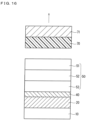
- FIG. 8 and FIG. 9 Described next using FIG. 8 and FIG. 9 is a step of fixing the nitride semiconductor layer on the diamond substrate to form the nitride semiconductor device. Firstly, in a step illustrated in FIG. 8 , the diamond substrate 10 illustrated in FIG. 2 is bonded to the nitride semiconductor layer 50 separated from the silicon carbide substrate 30.
Landscapes
- Chemical & Material Sciences (AREA)
- Organic Chemistry (AREA)
- Inorganic Chemistry (AREA)
- Engineering & Computer Science (AREA)
- Materials Engineering (AREA)
- Nanotechnology (AREA)
- Life Sciences & Earth Sciences (AREA)
- General Life Sciences & Earth Sciences (AREA)
- Geology (AREA)
- Recrystallisation Techniques (AREA)
- Junction Field-Effect Transistors (AREA)
Applications Claiming Priority (1)
| Application Number | Priority Date | Filing Date | Title |
|---|---|---|---|
| PCT/JP2020/012665 WO2021191956A1 (fr) | 2020-03-23 | 2020-03-23 | Dispositif à semi-conducteur au nitrure et son procédé de fabrication |
Publications (2)
| Publication Number | Publication Date |
|---|---|
| EP4131346A1 true EP4131346A1 (fr) | 2023-02-08 |
| EP4131346A4 EP4131346A4 (fr) | 2023-04-19 |
Family
ID=72829254
Family Applications (1)
| Application Number | Title | Priority Date | Filing Date |
|---|---|---|---|
| EP20926775.6A Pending EP4131346A4 (fr) | 2020-03-23 | 2020-03-23 | Dispositif à semi-conducteur au nitrure et son procédé de fabrication |
Country Status (6)
| Country | Link |
|---|---|
| US (1) | US12476165B2 (fr) |
| EP (1) | EP4131346A4 (fr) |
| JP (1) | JP6771706B1 (fr) |
| KR (1) | KR102731260B1 (fr) |
| CN (1) | CN115298807A (fr) |
| WO (1) | WO2021191956A1 (fr) |
Families Citing this family (6)
| Publication number | Priority date | Publication date | Assignee | Title |
|---|---|---|---|---|
| CN113594110B (zh) * | 2021-07-29 | 2024-04-16 | 东南大学苏州研究院 | 一种半导体器件及其制备方法 |
| TWI806457B (zh) * | 2022-03-01 | 2023-06-21 | 鴻創應用科技有限公司 | 複合基板及其製造方法 |
| CN115863399A (zh) * | 2023-02-24 | 2023-03-28 | 成都功成半导体有限公司 | 一种在金刚石衬底上键合GaN层的方法及其器件 |
| CN116314268A (zh) * | 2023-03-21 | 2023-06-23 | 西安电子科技大学 | 一种抑制自热效应的氮化镓器件及其制备方法 |
| CN117410013B (zh) * | 2023-12-14 | 2024-03-12 | 浙江正泰电器股份有限公司 | 一种石墨烯导体及石墨烯导体的制备方法 |
| WO2025243391A1 (fr) * | 2024-05-21 | 2025-11-27 | 三菱電機株式会社 | Dispositif à semi-conducteur et procédé de fabrication de dispositif à semi-conducteur |
Family Cites Families (17)
| Publication number | Priority date | Publication date | Assignee | Title |
|---|---|---|---|---|
| JP2009190918A (ja) | 2008-02-13 | 2009-08-27 | New Japan Radio Co Ltd | 窒化物半導体基板の製造方法及び窒化物半導体装置の製造方法 |
| US8409366B2 (en) | 2009-06-23 | 2013-04-02 | Oki Data Corporation | Separation method of nitride semiconductor layer, semiconductor device, manufacturing method thereof, semiconductor wafer, and manufacturing method thereof |
| JP5070247B2 (ja) | 2009-06-23 | 2012-11-07 | 株式会社沖データ | 半導体装置の製造方法、及び半導体装置 |
| US20110108854A1 (en) * | 2009-11-10 | 2011-05-12 | Chien-Min Sung | Substantially lattice matched semiconductor materials and associated methods |
| JP5545567B2 (ja) * | 2010-06-17 | 2014-07-09 | 国立大学法人金沢大学 | 単結晶ダイヤモンド成長用の基材及び単結晶ダイヤモンドの製造方法 |
| US20120141799A1 (en) * | 2010-12-03 | 2012-06-07 | Francis Kub | Film on Graphene on a Substrate and Method and Devices Therefor |
| JP5681959B2 (ja) * | 2010-12-07 | 2015-03-11 | 国立大学法人金沢大学 | グラフェン・ダイヤモンド積層体 |
| JP6098048B2 (ja) * | 2012-06-29 | 2017-03-22 | 株式会社豊田自動織機 | 半導体装置の製造方法 |
| WO2014030040A1 (fr) * | 2012-08-24 | 2014-02-27 | Soitec | Procédés de formation de structures et dispositifs semiconducteurs comprenant du graphène, et structures et dispositifs associés |
| JP2015015321A (ja) * | 2013-07-03 | 2015-01-22 | 高槻電器工業株式会社 | 半導体発光素子及びその製造方法 |
| CN103779193A (zh) * | 2014-01-27 | 2014-05-07 | 苏州能讯高能半导体有限公司 | 基于金刚石衬底的氮化物半导体器件及其制备方法 |
| CN119349566A (zh) | 2015-09-08 | 2025-01-24 | 麻省理工学院 | 基于石墨烯的层转移的系统和方法 |
| FR3061167B1 (fr) * | 2016-12-22 | 2019-07-05 | Commissariat A L'energie Atomique Et Aux Energies Alternatives | Procede de production d'un film de graphene |
| JP6930229B2 (ja) | 2017-06-05 | 2021-09-01 | 富士通株式会社 | 半導体装置の製造方法 |
| US10504722B2 (en) | 2017-07-25 | 2019-12-10 | United States Of America As Represented By The Secretary Of The Air Force | Growth of III-nitride semiconductors on thin van der Waals buffers for mechanical lift off and transfer |
| CN108878266B (zh) * | 2018-07-03 | 2020-09-08 | 北京大学 | 一种在多晶或非晶衬底上生长单晶氮化镓薄膜的方法 |
| CN109950131B (zh) * | 2019-02-28 | 2021-09-14 | 天津大学 | 以非极性晶面SiC为衬底的单层石墨烯及可控生长方法 |
-
2020
- 2020-03-23 WO PCT/JP2020/012665 patent/WO2021191956A1/fr not_active Ceased
- 2020-03-23 CN CN202080098651.2A patent/CN115298807A/zh active Pending
- 2020-03-23 EP EP20926775.6A patent/EP4131346A4/fr active Pending
- 2020-03-23 JP JP2020539304A patent/JP6771706B1/ja active Active
- 2020-03-23 US US17/799,272 patent/US12476165B2/en active Active
- 2020-03-23 KR KR1020227030438A patent/KR102731260B1/ko active Active
Also Published As
| Publication number | Publication date |
|---|---|
| JP6771706B1 (ja) | 2020-10-21 |
| EP4131346A4 (fr) | 2023-04-19 |
| US12476165B2 (en) | 2025-11-18 |
| WO2021191956A1 (fr) | 2021-09-30 |
| CN115298807A (zh) | 2022-11-04 |
| KR20220137070A (ko) | 2022-10-11 |
| US20230083507A1 (en) | 2023-03-16 |
| JPWO2021191956A1 (fr) | 2021-09-30 |
| KR102731260B1 (ko) | 2024-11-15 |
Similar Documents
| Publication | Publication Date | Title |
|---|---|---|
| US12476165B2 (en) | Nitride semiconductor device, and method of manufacturing nitride semiconductor device | |
| US10158009B2 (en) | Method of making a graphene base transistor with reduced collector area | |
| KR102403038B1 (ko) | 가공된 기판과 통합된 전자 전력 디바이스 | |
| US10134848B2 (en) | Semiconductor device having a graphene layer, and method of manufacturing thereof | |
| US8901536B2 (en) | Transistor having graphene base | |
| US20120056202A1 (en) | Semiconductor device | |
| US8703623B2 (en) | Fabrication technique for gallium nitride substrates | |
| US11576259B2 (en) | Carrier, laminate and method of manufacturing semiconductor devices | |
| TW200301016A (en) | Strain balanced nitride heterojunction transistors and methods of fabricating strain balanced nitride heterojunction transistors | |
| JP2007519262A5 (fr) | ||
| US11430875B2 (en) | Method for manufacturing transistor | |
| CN104798206B (zh) | 具有工程衬底的iii族氮化物晶体管 | |
| CN111211161A (zh) | 一种双向散热的纵向氮化镓功率晶体管及其制备方法 | |
| WO2017086253A1 (fr) | Élément électronique au diamant | |
| CN111863957A (zh) | 一种常闭型高电子迁移率晶体管及其制造方法 | |
| WO2019130546A1 (fr) | Dispositif à semi-conducteur au nitrure et son procédé de production | |
| CN112750898A (zh) | 基于氮化镓的半导体功率器件及其制造方法 | |
| KR101172857B1 (ko) | 인헨스먼트 노멀리 오프 질화물 반도체 소자 및 그 제조방법 | |
| US20240234139A9 (en) | Diamond-Capped Gallium Oxide Transistor | |
| JP5415668B2 (ja) | 半導体素子 | |
| JPWO2012099209A1 (ja) | 炭化ケイ素単結晶基板及び半導体素子の製造方法 | |
| JP7656701B2 (ja) | 高電子移動度を有するトランジスタを製造する方法及び製造したトランジスタ | |
| CN101322229A (zh) | 半导体soi器件 | |
| Mehta | Development of FETs based on ultra-wide band gap materials for high voltage power electronics | |
| JP2024179648A (ja) | 窒化物半導体装置および窒化物半導体装置の製造方法 |
Legal Events
| Date | Code | Title | Description |
|---|---|---|---|
| STAA | Information on the status of an ep patent application or granted ep patent |
Free format text: STATUS: THE INTERNATIONAL PUBLICATION HAS BEEN MADE |
|
| PUAI | Public reference made under article 153(3) epc to a published international application that has entered the european phase |
Free format text: ORIGINAL CODE: 0009012 |
|
| STAA | Information on the status of an ep patent application or granted ep patent |
Free format text: STATUS: REQUEST FOR EXAMINATION WAS MADE |
|
| 17P | Request for examination filed |
Effective date: 20220913 |
|
| AK | Designated contracting states |
Kind code of ref document: A1 Designated state(s): AL AT BE BG CH CY CZ DE DK EE ES FI FR GB GR HR HU IE IS IT LI LT LU LV MC MK MT NL NO PL PT RO RS SE SI SK SM TR |
|
| A4 | Supplementary search report drawn up and despatched |
Effective date: 20230321 |
|
| RIC1 | Information provided on ipc code assigned before grant |
Ipc: H01L 29/66 20060101ALI20230315BHEP Ipc: C01B 32/28 20170101ALI20230315BHEP Ipc: C01B 32/184 20170101ALI20230315BHEP Ipc: H01L 21/20 20060101ALI20230315BHEP Ipc: H01L 29/812 20060101ALI20230315BHEP Ipc: H01L 29/778 20060101ALI20230315BHEP Ipc: H01L 21/338 20060101AFI20230315BHEP |
|
| DAV | Request for validation of the european patent (deleted) | ||
| DAX | Request for extension of the european patent (deleted) | ||
| STAA | Information on the status of an ep patent application or granted ep patent |
Free format text: STATUS: EXAMINATION IS IN PROGRESS |
|
| 17Q | First examination report despatched |
Effective date: 20260204 |
|
| STAA | Information on the status of an ep patent application or granted ep patent |
Free format text: STATUS: THE APPLICATION HAS BEEN WITHDRAWN |