EP4131354A1 - Halbleiterstruktur und herstellungsverfahren dafür - Google Patents
Halbleiterstruktur und herstellungsverfahren dafür Download PDFInfo
- Publication number
- EP4131354A1 EP4131354A1 EP21931178.4A EP21931178A EP4131354A1 EP 4131354 A1 EP4131354 A1 EP 4131354A1 EP 21931178 A EP21931178 A EP 21931178A EP 4131354 A1 EP4131354 A1 EP 4131354A1
- Authority
- EP
- European Patent Office
- Prior art keywords
- patterns
- mask
- mask patterns
- sacrificial
- dielectric layer
- Prior art date
- Legal status (The legal status is an assumption and is not a legal conclusion. Google has not performed a legal analysis and makes no representation as to the accuracy of the status listed.)
- Pending
Links
Images




Classifications
-
- H—ELECTRICITY
- H10—SEMICONDUCTOR DEVICES; ELECTRIC SOLID-STATE DEVICES NOT OTHERWISE PROVIDED FOR
- H10P—GENERIC PROCESSES OR APPARATUS FOR THE MANUFACTURE OR TREATMENT OF DEVICES COVERED BY CLASS H10
- H10P76/00—Manufacture or treatment of masks on semiconductor bodies, e.g. by lithography or photolithography
- H10P76/40—Manufacture or treatment of masks on semiconductor bodies, e.g. by lithography or photolithography of masks comprising inorganic materials
- H10P76/405—Manufacture or treatment of masks on semiconductor bodies, e.g. by lithography or photolithography of masks comprising inorganic materials characterised by their composition, e.g. multilayer masks
-
- H—ELECTRICITY
- H10—SEMICONDUCTOR DEVICES; ELECTRIC SOLID-STATE DEVICES NOT OTHERWISE PROVIDED FOR
- H10B—ELECTRONIC MEMORY DEVICES
- H10B12/00—Dynamic random access memory [DRAM] devices
- H10B12/01—Manufacture or treatment
- H10B12/02—Manufacture or treatment for one transistor one-capacitor [1T-1C] memory cells
- H10B12/03—Making the capacitor or connections thereto
- H10B12/033—Making the capacitor or connections thereto the capacitor extending over the transistor
-
- H—ELECTRICITY
- H10—SEMICONDUCTOR DEVICES; ELECTRIC SOLID-STATE DEVICES NOT OTHERWISE PROVIDED FOR
- H10P—GENERIC PROCESSES OR APPARATUS FOR THE MANUFACTURE OR TREATMENT OF DEVICES COVERED BY CLASS H10
- H10P50/00—Etching of wafers, substrates or parts of devices
- H10P50/73—Etching of wafers, substrates or parts of devices using masks for insulating materials
-
- H—ELECTRICITY
- H10—SEMICONDUCTOR DEVICES; ELECTRIC SOLID-STATE DEVICES NOT OTHERWISE PROVIDED FOR
- H10P—GENERIC PROCESSES OR APPARATUS FOR THE MANUFACTURE OR TREATMENT OF DEVICES COVERED BY CLASS H10
- H10P76/00—Manufacture or treatment of masks on semiconductor bodies, e.g. by lithography or photolithography
- H10P76/40—Manufacture or treatment of masks on semiconductor bodies, e.g. by lithography or photolithography of masks comprising inorganic materials
- H10P76/408—Manufacture or treatment of masks on semiconductor bodies, e.g. by lithography or photolithography of masks comprising inorganic materials characterised by their sizes, orientations, dispositions, behaviours or shapes
- H10P76/4085—Manufacture or treatment of masks on semiconductor bodies, e.g. by lithography or photolithography of masks comprising inorganic materials characterised by their sizes, orientations, dispositions, behaviours or shapes characterised by the processes involved to create the masks
-
- H—ELECTRICITY
- H10—SEMICONDUCTOR DEVICES; ELECTRIC SOLID-STATE DEVICES NOT OTHERWISE PROVIDED FOR
- H10W—GENERIC PACKAGES, INTERCONNECTIONS, CONNECTORS OR OTHER CONSTRUCTIONAL DETAILS OF DEVICES COVERED BY CLASS H10
- H10W20/00—Interconnections in chips, wafers or substrates
- H10W20/01—Manufacture or treatment
- H10W20/071—Manufacture or treatment of dielectric parts thereof
- H10W20/081—Manufacture or treatment of dielectric parts thereof by forming openings in the dielectric parts
- H10W20/084—Manufacture or treatment of dielectric parts thereof by forming openings in the dielectric parts for dual-damascene structures
- H10W20/087—Manufacture or treatment of dielectric parts thereof by forming openings in the dielectric parts for dual-damascene structures involving multiple stacked pre-patterned masks
Definitions
- the present application relates to a semiconductor structure and a method for forming a semiconductor structure.
- Dimensional uniformity is an important technical index of semiconductor manufacturing process.
- the improvement of dimensional uniformity plays an important role in improving process window and product yield.
- the dimensional uniformity of capacitance holes in Dynamic Random Access Memory, DRAM is particularly critical to the performance of the product.
- the dimensional uniformity of capacitance holes in the related art still needs to be improved.
- the present application provides a method for forming a semiconductor structure, which includes the following operations.
- a base is provided.
- a first dielectric layer is formed on the base.
- a plurality of first mask patterns each having zigzag shape are formed on the first dielectric layer, in which the first mask patterns extend in a first direction.
- a plurality of second mask patterns each having zigzag shape are formed on the first mask patterns, in which the second mask patterns extend in a second direction different from the first direction, and projections of the first mask patterns on the first dielectric layer and projections of the second mask patterns on the first dielectric layer overlap with each other to form polygons.
- the first dielectric layer is etched by using the second mask patterns and the first mask patterns as masks to form openings.
- the present application further provides a semiconductor structure, which includes:
- the present application provides a semiconductor structure and a method for forming a semiconductor structure.
- the method for forming the semiconductor structure includes the following operations.
- a base is provided.
- a first dielectric layer is formed on the base.
- a plurality of first mask patterns each having zigzag shape are formed on the first dielectric layer, in which the first mask patterns extend in a first direction.
- a plurality of second mask patterns each having zigzag shape are formed on the first mask patterns, in which the second mask patterns extend in a second direction different from the first direction, and projections of the first mask patterns on the first dielectric layer and projections of the second mask patterns on the first dielectric layer overlap with each other to form polygons.
- the first dielectric layer is etched by using the second mask patterns and the first mask patterns as masks to form openings.
- the polygonal shape is defined by the cooperation between the first mask patterns each having zigzag shape and the second mask patterns each having zigzag shape, and the openings are formed by etching the first dielectric layer by using the first mask patterns and the second mask patterns as masks, so that the etching uniformity problem caused by the etching load effect may be improved.
- a base 200 is provided.
- the base 200 may be served as a platform for subsequent processes.
- the base 200 includes a semiconductor substrate 201 and at least one interlayer dielectric layer 202 arranged on the semiconductor substrate 201.
- a connection pad 220 may be formed in the interlayer dielectric layer 202.
- the connection pad 202 may be subsequently configured to be connected to an electrode of a capacitor formed in a capacitance hole.
- the material of the semiconductor substrate 201 may be silicon (Si), germanium (Ge), silicon germanium (GeSi), or silicon carbide (SiC); it may also be Silicon On Insulator, SOI, or Germanium On Insulator, GOI. Alternatively, it may be other materials, for example, group III-V compounds, such as gallium arsenide.
- the material of the semiconductor substrate 201 in this embodiment is silicon.
- the semiconductor substrate is doped with certain impurity ions as required, and the impurity ions may be N-type impurity ions or P-type impurity ions.
- a plurality of trench type transistors may be formed in the semiconductor substrate 201, and each of the trench type transistors includes an active region.
- the active region is at least provided with one trench, and the active region is divided into a drain region and at least one source region by the trench. Specifically, when therein is one trench, the active region is divided into a source region and a drain region respectively arranged on both sides of the trench by the trench.
- the two trenches are parallel to each other, and the active region is divided into a drain region arranged between the two trenches and two source regions respectively arranged on the outside of the two trenches by the two trenches.
- a gate structure or word line, WL is arranged in the trench.
- connection pad 220 formed in the interlayer dielectric layer is connected to the respective source region.
- the connection pad 220 may be connected to the respective source region through a metal connection plug or a semiconductor connection plug.
- the interlayer dielectric layer 202 may be a single layer or a multilayer (two or more layers) stacked structure.
- the material of the interlayer dielectric layer may be silicon nitride, silicon oxynitride, silicon oxide, fluorine-doped silicon dioxide, FSG, boron-doped silicon dioxide, BSG, phosphorus-doped silicon dioxide, PSG, or boron-phosphorus-doped silicon dioxide, BPSG, a low dielectric material, other suitable materials, and/or a combination thereof.
- a first dielectric layer 205 is formed on the base 200.
- the first dielectric layer 205 may be configured to define and support a functional structure subsequently formed, such as a capacitance structure.
- the first dielectric layer 205 may be a single layer or multilayer stacked structure.
- the material of the first dielectric layer 205 may be any one of silicon oxide, silicon nitride, silicon oxynitride, silicon oxycarbide, or silicon carbide nitride.
- the multilayer stacked structure may include several supporting layers and sacrificial layers alternately stacked onto one another.
- the material of the sacrificial layer is different from the material of the supporting layer.
- the material of the sacrificial layer may include any one of silicon oxide, silicon oxynitride, silicon oxycarbide, silicon carbide nitride, fluorine-doped silicon dioxide, FSG, boron-doped silicon dioxide, BSG, phosphorus-doped silicon dioxide, PSG, or boron-phosphorus-doped silicon dioxide, BPSG.
- the material of the supporting layer includes silicon nitride or doped silicon nitride, such as boron-doped or phosphorus-doped silicon nitride.
- the first dielectric layer 205 includes a first supporting layer, a first sacrificial layer, a second supporting layer, a second sacrificial layer and a third supporting layer sequentially stacked onto one another on the base 200.
- the materials of the first sacrificial layer and the second sacrificial layer include any one of silicon oxide, silicon oxynitride, silicon oxycarbide, silicon carbide nitride, fluorine-doped silicon dioxide, FSG, boron-doped silicon dioxide, BSG, phosphorus-doped silicon dioxide, PSG, or boron-phosphorus-doped silicon dioxide, BPSG.
- the materials of the first supporting layer, the second supporting layer and the third supporting layer include silicon nitride or doped silicon nitride, such as boron-doped or phosphorus-doped silicon nitride.
- the materials of the first sacrificial layer and the second sacrificial layer may be the same or different, and the materials of the first supporting layer, the second supporting layer and the third supporting layer may be the same or different.
- the thickness of the first dielectric layer 205 is comprised between 500 nm and 3000 nm.
- a plurality of first mask patterns 209 each having zigzag shape are formed on the first dielectric layer 205.
- the first mask patterns 209 extend in the first direction D1.
- the plurality of first mask patterns 209 extend along the first direction D1, and are arranged adjacent to each other on the first dielectric layer 205.
- each first mask pattern 209 has sawteeth. Specifically, each sawtooth has a same angle, for example, 120°. Each sawtooth may also have a same length.
- each two adjacent first mask patterns 209 are axisymmetric patterns. As illustrated in FIG. 7 , each two adjacent first mask patterns 209 are axially symmetrical about a first symmetry axis A1. The first symmetry axis A1 is located in the middle of the two adjacent first mask patterns 209 and parallel to the first direction D1.
- a method for forming the first mask patterns is described in detail below with reference to a specific embodiment.
- FIG. 4 is a schematic top view of FIG. 3 .
- a plurality of first sacrificial patterns 207 which are separated from each other and extend in the first direction D1, are formed on the first dielectric layer 205.
- Each first sacrificial pattern 207 includes sidewalls 11 each having zigzag shape on both sides of each first sacrificial pattern 207.
- the plurality of first sacrificial patterns 207 extend in the first direction D1 and is arranged adjacent to each other.
- the adjacent first sacrificial patterns 207 may be arranged adjacent to each other in parallel at equal intervals, and each first sacrificial pattern 207 includes sidewalls 11 each having symmetrical zigzag shape on both sides of each first sacrificial pattern 207.
- each first sacrificial pattern 207 may be a photoresist. Specifically, a photoresist is spin-coated on the first dielectric layer 205, and a photoresist pattern having zigzag shape is formed through exposure and development. In other examples, the material of each first sacrificial pattern 207 may be polysilicon, amorphous silicon, amorphous carbon, or the like. Specifically, a first mask sacrificial layer is formed on the first dielectric layer 205. A photoresist is spin-coated on the first mask sacrificial layer. A photoresist pattern having zigzag shape is formed through exposure and development.
- the first mask sacrificial layer is etched by using the photoresist pattern, so as to form the first sacrificial patterns 207.
- a plurality of first sacrificial patterns 207 which are separated from each other and extend along the first direction D1 may be formed, and the distances between the centers of two adjacent first sacrificial patterns 207 may be equal to each other.
- the first direction D1 is parallel to the direction of X-axis, and a plurality of first sacrificial patterns 207 separated from each other may be arranged at equal intervals in the direction of Y-axis.
- the shapes of the sidewalls of the first sacrificial patterns 207 define the shapes of the first mask patterns subsequently formed.
- the first sacrificial patterns 207 may include sidewalls 11 each having symmetrical zigzag shape. Specifically, each of the sidewalls 11 on both sides of each first sacrificial pattern 207 has zigzag shape, and the sidewalls 11 on both sides of each first sacrificial patterns 207 are axially symmetrical about the symmetry axis A1 (with reference to FIG. 4 ).
- the zigzag shape of each of the sidewalls 11 of each first sacrificial pattern 207 has sawteeth.
- Each sawtooth has the same angle or the same length, or each sawtooth has the same angle and the same length.
- each first mask pattern subsequently formed also has zigzag shape
- the zigzag shape of each first mask pattern also has sawteeth
- each sawtooth has the same angle or the same length, or each sawtooth has the same angle and the same length.
- the angle of each sawtooth is 120°.
- first sidewall layers 208 are formed on the sidewalls and the top portions of the first sacrificial patterns 207 and on the first dielectric layer 205 between the adjacent first sacrificial patterns 207.
- the first sidewall layers 208 are configured to subsequently form the first mask patterns.
- the material of the first sidewall layer 208 is different from the material of the first sacrificial pattern 207.
- Each first sidewall layer 208 has a higher etching selection ratio with respect to the first sacrificial patterns 207, so that the first sidewall layers 208 may be selectively etched through a dry etching process, thereby improving the accuracy of the positions and shapes of the formed first mask patterns 209.
- the first mask patterns 209 will not be excessively damaged during subsequent removal of the first sacrificial patterns 207.
- the material of the first sidewall layer 208 may be one of silicon oxide, silicon nitride, silicon oxynitride, silicon oxycarbide, or silicon carbide nitride.
- the first sidewall layers 208 may be formed through the PVD or ALD process.
- the first sidewall layers 208 with thinner thickness, such as 1 ⁇ -200 ⁇ , may be formed through the ALD process.
- a first hard mask layer 206 is formed on the first dielectric layer 205. A portion of the first sidewall layers 208 are arranged on the surface of the first hard mask layer 206. Specifically, a first hard mask layer 206 is formed on the first dielectric layer 205, and the first sacrificial patterns 207 are arranged on the first hard mask layer 206.
- the first hard mask layer 206 is etched by using the first sidewall layers 209 remaining on the sidewalls of the first sacrificial patterns 207, so as to form the first mask patterns. Specifically, the first hard mask layer 206 arranged below the first sidewall layers 209 remaining on the sidewalls of the first sacrificial patterns 207 form the first mask patterns.
- the first sidewall layers 208 on the top portions of the first sacrificial patterns 207 and the first sidewall layers 208 between the adjacent first sacrificial patterns 207 are removed, so that the first sidewall layers 208 remaining on the sidewalls of the first sacrificial patterns 207 form the first mask patterns 209.
- an anisotropic dry etching process may be used.
- the first sidewall layers 208 on the top portions of the first sacrificial patterns 207 and the first sidewall layers 208 between the adjacent first sacrificial patterns 207 are removed through the etching selection ratio of the first sacrificial pattern 207 to the first sidewall layer 208, so that the first sidewall layers 208 on the sidewalls of the first sacrificial patterns 207 are remained to form the first mask patterns 209.
- each formed first mask pattern 209 has sawteeth.
- Each sawtooth has the same angle or the same length, or each sawtooth has the same angle and the same length.
- the angle of each sawtooth is 120°
- each two adjacent first mask patterns 209 among the plurality of first mask patterns 209 each having zigzag shape are axisymmetric patterns.
- two adjacent first mask patterns 209 on the sidewalls of a single first sacrificial pattern 207 are axially symmetrical about the first symmetry axis A1.
- the first symmetry axis A1 is located in the middle of the two adjacent first mask patterns 209 and parallel to the first direction D1.
- the dimensions of the first mask patterns 209 formed by the above-mentioned method are relatively small.
- thinner first sidewall layers 208 may be conformally formed on the first sacrificial patterns 207 through the ALD process, and the second mask patterns with smaller dimensions may be subsequently formed on the first mask patterns through the same process, so that openings having thinner sidewall thickness and better dimensional uniformity may be formed when the first dielectric layer 205 is etched by using the first mask patterns 209 and the second mask patterns, thereby improving the density and quality of the openings.
- the first sacrificial patterns 207 may be removed by a wet or dry process.
- the first sacrificial patterns 207 may be removed through an ashing process.
- subsequent operations of forming the second mask patterns may be directly performed without removing the first sacrificial patterns 207.
- a plurality of second mask patterns 213 each having zigzag shape are formed on the first mask patterns 209.
- the plurality of second mask patterns 213 each having zigzag shape extend in the second direction D2 different from the first direction D1.
- the projections of the plurality of first mask patterns 209 each having zigzag shape on the first dielectric layer 205 and the projections of the plurality of second mask patterns 213 each having zigzag shape on the first dielectric layer 205 overlap with each other, so as to form polygons.
- a method for forming the second mask patterns is described in detail below with reference to a specific embodiment.
- a covering layer 210 is formed on the first mask patterns 209.
- the covering layer 210 has a flat surface.
- the covering layer 210 may be a single layer or multilayer stacked structure.
- the second sacrificial patterns are subsequently formed on the covering layer 210.
- the covering layer 210 may include a first covering layer filling the gap between the first mask patterns 209, and a second covering layer arranged on the first covering layer.
- the second sacrificial patterns are subsequently formed on the second covering layer.
- a second hard mask layer may also be formed on the surface of the covering layer 210.
- the second sacrificial patterns are subsequently formed on the second hard mask layer.
- the material of the covering layer 210 is different from the material of the first mask pattern 209.
- the material of the covering layer 210 may contain carbon or silicon oxide.
- each second sacrificial pattern 211 includes sidewalls 12 each having zigzag shape on both sides of each second sacrificial pattern 211.
- each second sacrificial pattern 211 includes sidewalls 12 each having symmetrical zigzag shape on both sides of each second sacrificial pattern 211.
- the material of the second sacrificial pattern 211 may be a photoresist or other suitable material (such as polysilicon, amorphous silicon, or amorphous carbon).
- a plurality of second sacrificial patterns 211 separated from each other may be formed through exposure and development processes, or through exposure, development, and etching processes.
- the plurality of second sacrificial patterns 211 separated from each other extend parallel to the second direction D2, and the distances between the centers of two adjacent second sacrificial patterns 211 are equal to each other.
- an angle B between the second direction D2 and the first direction D1 is 60°.
- the shapes of the sidewalls of the second sacrificial patterns 211 define the shapes of second mask patterns subsequently formed.
- the second sacrificial patterns 211 include sidewalls 12 each having symmetrical zigzag shape. Specifically, each of the sidewalls 12 on both sides of each second sacrificial pattern 211 has zigzag shape, and the sidewalls 12 on both sides of each second sacrificial patterns 211 are axially symmetrical about the symmetry axis A2 (with reference to FIG. 11 )
- the zigzag shape of each of the sidewalls 12 of each second sacrificial pattern 211 has sawteeth.
- Each sawtooth has the same angle or the same length, or each sawtooth has the same angle and the same length.
- each second mask pattern subsequently formed also has zigzag shape, the zigzag shape of each second mask pattern also has sawteeth, and each sawtooth has the same angle or the same length, or each sawtooth has the same angle and the same length.
- the angle of each sawtooth is 120°.
- second sidewall layers 212 are formed on the sidewalls and the top portions of the second sacrificial patterns 211 and on the covering layer 210 between the adjacent second sacrificial patterns 211.
- the second sidewall layers 212 are configured to subsequently form the second mask patterns.
- the material of the second sidewall layer 212 is different from the material of the second sacrificial pattern 211.
- Each second sidewall layer 212 has a higher etching selection ratio with respect to the second sacrificial patterns 211, so that the second sidewall layers 212 may be selectively etched through a dry etching process, thereby improving the accuracy of the positions and shapes of the formed second mask patterns 213.
- the second mask patterns 213 will not be excessively damaged during subsequent removal of the second sacrificial patterns 211.
- the material of the second sidewall layer 212 may be any one of silicon oxide, silicon nitride, silicon oxynitride, silicon oxycarbide, or silicon carbide nitride.
- the second sidewall layers 212 are formed through the CVD or ALD process.
- the second sidewall layers 212 with thinner thickness, such as 1 ⁇ -200 ⁇ , may be formed through the ALD process.
- a portion of the second sidewall layers 212 are arranged on the surface of the second hard mask layer.
- the second sidewall layers 212 on the top portions of the second sacrificial patterns 211 and on the covering layer 210 are removed, so that the second sidewall layers 212 remaining on the sidewalls of the second sacrificial patterns 211form the second mask patterns 213.
- the second sidewall layers 212 on the top portions of the second sacrificial patterns 211 and on the covering layer 210 may be removed by using an anisotropic dry etching process, so that the second sidewall layers 212 on the sidewalls of the second sacrificial patterns 211 are remained to form second mask patterns 213.
- Each formed second mask pattern 213 has zigzag shape.
- the zigzag shape of each second mask pattern has sawteeth.
- Each sawtooth has the same angle or the same length, or each sawtooth has the same angle and the same length.
- the angle of each sawtooth is 120°
- each two adjacent second mask patterns 213 among the plurality of second mask patterns 213 each having zigzag shape are axisymmetric patterns.
- two adjacent second mask patterns 213 among the plurality of second mask patterns 213 each having zigzag shape are axially symmetrical about the second symmetry axis A2.
- the second symmetry axis A2 is located in the middle of the two adjacent second mask patterns 213 and parallel to the second direction D2.
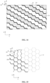
- the projection of an edge of each sawtooth in each second mask pattern 213 on the first dielectric layer coincides with the projection of an edge of a respective sawtooth in each first mask pattern 209 on the first dielectric layer, so that the projection 209T of the plurality of first mask patterns 209 each having zigzag shape on the first dielectric layer and the projection 213T of the plurality of second mask patterns 213 each having zigzag shape on the first dielectric layer overlap with each other, so as to form a plurality of regular hexagons 13 arranged in a honeycomb shape (with reference to FIG. 15 ).
- the openings subsequently formed by etching the first dielectric layer 205 through the first mask patterns 209 and the second mask patterns 213 are also arranged in a honeycomb shape.
- the second sacrificial patterns 211 are removed.
- the second sacrificial patterns 211 may be removed through wet etching or dry etching.
- the second sacrificial patterns 211 may be removed through an ashing process.
- the first dielectric layer 205 is etched by using a plurality of second mask patterns 213 each having zigzag shape and a plurality of first mask patterns 209 each having zigzag shape as masks, so as to form a plurality of openings 215 in the first dielectric layer 205.
- the openings may be capacitance holes.
- the first dielectric layer 205 may be etched by using an anisotropic dry etching process.
- the gases used for etching the first dielectric layer 205 include one or more of CF4, C4F8, and CHF3.
- the openings 215 are formed in a regular hexagonal shape, and a plurality of regular hexagonal openings 215 are arranged in a honeycomb shape (with reference to FIG. 18 ).
- the shape of the regular hexagon is defined by the first mask patterns and the second mask patterns in an above-mentioned specific shape.
- the load effect during etching may be better prevented, so that the formed openings 215 have better dimensional uniformity, thereby facilitating the improvement of the production yield and performance of chip.
- the dimensions of the first mask patterns and the second mask patterns may be made smaller, so that the thickness of the sidewalls of the openings 215 in a regular hexagonal shape may be thinner, thereby increasing the density of the openings 215 formed per unit area.
- Another embodiment of the present application further provides a method for forming a semiconductor structure.
- the specific value of the angle B between the extending direction of each first mask pattern and the extending direction of each second mask pattern is different from the specific value of the angles B between the extending direction of each first mask pattern and the extending direction of each second mask pattern in the above-mentioned embodiment.
- Other definitions and descriptions are the same as those in the above-mentioned embodiment, which are not repeated herein.
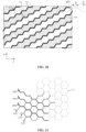
- the detail description may refer to FIG. 19 to FIG. 21 .
- the first mask patterns 209 extend along the first direction D1.
- the second mask patterns 213 extend along the second direction D2.
- the angle between the first direction D1 and the second direction D2 is 120°.
- projections 209T of a plurality of first mask patterns 209 each having zigzag shape on the first dielectric layer and the projections 213T of a plurality of second mask patterns 213 each having zigzag shape on the first dielectric layer overlap with each other, so as to form a plurality of regular hexagons 13 arranged in a honeycomb shape.
- the present application further provides a semiconductor structure.
- the semiconductor structure includes:
- the zigzag shape of each first mask pattern 209 and the zigzag shape of each second mask patterns 213 have sawteeth.
- each sawtooth has a same angle or a same length, or each sawtooth has the same angle and the same length.
- the angle of each sawtooth may be 120°.
- each two adjacent first mask patterns 209 are axisymmetric patterns, or each two adjacent second mask patterns 213 are axisymmetric patterns.
- two adjacent first mask patterns 209 among the plurality of first mask patterns 209 each having zigzag shape are axially symmetrical about a first symmetry axis A1.
- the first symmetry axis A1 is located in the middle of the two adjacent first mask patterns 209 and parallel to the first direction D1 (with reference to FIG. 7 ).
- Two adjacent second mask patterns 213 among the plurality of second mask patterns 213 each having zigzag shape are axially symmetrical about a second symmetry axis A2.
- the second symmetry axis A2 is located in the middle of the two adjacent second mask patterns and parallel to the second direction D2 (with reference to FIG. 14 ).
- the angle between the first direction D1 and the second direction D2 is 60° or 120°, and each polygon is a regular hexagon.
- a projection of an edge of each sawtooth in each second mask pattern 213 on the first dielectric layer 205 coincides with a projection of an edge of a respective sawtooth in each first mask pattern 209 on the first dielectric layer 205.
- the embodiments of the present application provide a semiconductor structure and a method for forming a semiconductor structure.
- the polygonal shape is defined by the cooperation between the first mask patterns each having zigzag shape and the second mask patterns each having zigzag shape, and the openings are formed by etching the first dielectric layer by using the first mask patterns and the second mask patterns as masks, so that the etching uniformity problem caused by the etching load effect may be improved.
Landscapes
- Engineering & Computer Science (AREA)
- Manufacturing & Machinery (AREA)
- Drying Of Semiconductors (AREA)
- Semiconductor Memories (AREA)
Applications Claiming Priority (2)
| Application Number | Priority Date | Filing Date | Title |
|---|---|---|---|
| CN202110289168.9A CN115116959B (zh) | 2021-03-18 | 2021-03-18 | 半导体结构及其形成方法 |
| PCT/CN2021/120121 WO2022193603A1 (zh) | 2021-03-18 | 2021-09-24 | 半导体结构及其形成方法 |
Publications (2)
| Publication Number | Publication Date |
|---|---|
| EP4131354A1 true EP4131354A1 (de) | 2023-02-08 |
| EP4131354A4 EP4131354A4 (de) | 2023-12-13 |
Family
ID=83284176
Family Applications (1)
| Application Number | Title | Priority Date | Filing Date |
|---|---|---|---|
| EP21931178.4A Pending EP4131354A4 (de) | 2021-03-18 | 2021-09-24 | Halbleiterstruktur und herstellungsverfahren dafür |
Country Status (2)
| Country | Link |
|---|---|
| US (1) | US12278107B2 (de) |
| EP (1) | EP4131354A4 (de) |
Family Cites Families (22)
| Publication number | Priority date | Publication date | Assignee | Title |
|---|---|---|---|---|
| US7358146B2 (en) * | 2003-06-24 | 2008-04-15 | Micron Technology, Inc. | Method of forming a capacitor |
| US7153778B2 (en) | 2004-02-20 | 2006-12-26 | Micron Technology, Inc. | Methods of forming openings, and methods of forming container capacitors |
| KR100594326B1 (ko) * | 2005-03-22 | 2006-06-30 | 삼성전자주식회사 | 2-비트 동작을 위한 비휘발성 메모리 소자 및 그 제조 방법 |
| US9152039B2 (en) * | 2011-10-18 | 2015-10-06 | Taiwan Semiconductor Manufacturing Company, Ltd. | Multiple patterning technology method and system for achieving minimal pattern mismatch |
| KR101883327B1 (ko) * | 2012-03-28 | 2018-07-30 | 삼성전자주식회사 | 반도체 소자의 미세 패턴 형성 방법 |
| KR102065481B1 (ko) * | 2012-12-06 | 2020-01-13 | 삼성전자주식회사 | 반도체 소자의 미세 패턴 형성 방법 |
| KR102064265B1 (ko) * | 2013-06-20 | 2020-01-09 | 삼성전자주식회사 | 패드 형성 방법, 이를 이용한 반도체 장치 제조 방법, 도전성 패드 어레이 및 이를 포함하는 반도체 장치 |
| KR102219460B1 (ko) * | 2014-09-04 | 2021-02-24 | 삼성전자주식회사 | 반도체 장치의 레이아웃 분리 방법 및 이를 사용한 반도체 장치 제조 방법 |
| KR102414612B1 (ko) * | 2015-10-13 | 2022-07-01 | 삼성전자주식회사 | 반도체 소자 및 그 제조 방법 |
| KR102606308B1 (ko) * | 2016-06-28 | 2023-11-24 | 삼성전자주식회사 | 포토 마스크의 제조 방법, 패턴 형성 방법 및 반도체 장치의 제조 방법 |
| CN108155149B (zh) | 2016-12-02 | 2020-10-30 | 中芯国际集成电路制造(上海)有限公司 | 鳍式场效应管的形成方法以及半导体结构 |
| US11901190B2 (en) * | 2017-11-30 | 2024-02-13 | Taiwan Semiconductor Manufacturing Company, Ltd. | Method of patterning |
| CN110634733B (zh) | 2018-06-22 | 2024-10-25 | 长鑫存储技术有限公司 | 半导体存储器电容孔的制备方法 |
| US10790155B2 (en) * | 2018-06-27 | 2020-09-29 | Taiwan Semiconductor Manufacturing Co., Ltd. | Method of manufacturing semiconductor devices |
| CN111199875B (zh) | 2018-11-16 | 2022-03-15 | 长鑫存储技术有限公司 | 图形化硬掩膜层制备方法、电容器阵列结构及其制备方法 |
| KR102778777B1 (ko) * | 2019-01-07 | 2025-03-11 | 삼성전자주식회사 | 패턴 형성 방법 및 이를 이용한 반도체 장치의 제조 방법 |
| CN111524795B (zh) | 2019-02-03 | 2024-02-27 | 中芯国际集成电路制造(上海)有限公司 | 自对准双重图形化方法及其形成的半导体结构 |
| CN112349588B (zh) | 2019-08-07 | 2023-11-10 | 中芯国际集成电路制造(上海)有限公司 | 半导体结构的形成方法、晶体管 |
| CN120936025A (zh) | 2019-09-27 | 2025-11-11 | 福建省晋华集成电路有限公司 | 半导体器件 |
| WO2022052040A1 (en) * | 2020-09-11 | 2022-03-17 | Yangtze Memory Technologies Co., Ltd. | Method of forming top select gate trenches |
| KR102899927B1 (ko) * | 2021-07-27 | 2025-12-15 | 삼성전자주식회사 | 반도체 소자 |
| US11892774B2 (en) * | 2021-08-30 | 2024-02-06 | Taiwan Semiconductor Manufacturing Company, Ltd. | Lithography |
-
2021
- 2021-09-24 EP EP21931178.4A patent/EP4131354A4/de active Pending
-
2022
- 2022-02-21 US US17/676,293 patent/US12278107B2/en active Active
Also Published As
| Publication number | Publication date |
|---|---|
| US20220301871A1 (en) | 2022-09-22 |
| EP4131354A4 (de) | 2023-12-13 |
| US12278107B2 (en) | 2025-04-15 |
Similar Documents
| Publication | Publication Date | Title |
|---|---|---|
| US8399916B2 (en) | Semiconductor device and manufacturing method thereof | |
| US8637364B2 (en) | Semiconductor device and method of manufacturing the same | |
| US8120103B2 (en) | Semiconductor device with vertical gate and method for fabricating the same | |
| US7387930B2 (en) | Method of fabricating a bottle trench and a bottle trench capacitor | |
| US20040266101A1 (en) | Storage node contact forming method and structure for use in semiconductor memory | |
| US11690213B2 (en) | Semiconductor devices having a decreasing height gate structure | |
| CN114005791B (zh) | 存储器件及其形成方法 | |
| US12342535B2 (en) | Memory forming method and memory | |
| KR20210018683A (ko) | 지지 패턴을 포함하는 반도체 소자 및 이의 제조 방법 | |
| JP3640763B2 (ja) | 半導体メモリ素子のキャパシタの製造方法 | |
| US20160027743A1 (en) | Semiconductor device | |
| CN115116959B (zh) | 半导体结构及其形成方法 | |
| US12278107B2 (en) | Semiconductor structure and method for forming semiconductor structure | |
| US11723185B2 (en) | Capacitor structure, method for manufacturing same, and memory | |
| US7638827B2 (en) | Semiconductor memory device | |
| KR100744218B1 (ko) | 하나 이상의 커패시터를 포함하는 집적 회로 및 그 제조방법 | |
| TWI695485B (zh) | 埋入式字元線結構 | |
| WO2022028175A1 (zh) | 一种存储器的形成方法和存储器 | |
| US20260047074A1 (en) | Semiconductor device | |
| US11889677B2 (en) | Method for forming capacitor holes | |
| CN114068536B (zh) | 一种半导体器件及其制造方法 | |
| TWI856426B (zh) | 半導體結構的形成方法及半導體結構 | |
| KR100870338B1 (ko) | 반도체 소자의 커패시터 및 커패시터의 제조 방법 | |
| TW202439933A (zh) | 半導體裝置 | |
| CN120692845A (zh) | 半导体装置与其制作方法 |
Legal Events
| Date | Code | Title | Description |
|---|---|---|---|
| STAA | Information on the status of an ep patent application or granted ep patent |
Free format text: STATUS: THE INTERNATIONAL PUBLICATION HAS BEEN MADE |
|
| PUAI | Public reference made under article 153(3) epc to a published international application that has entered the european phase |
Free format text: ORIGINAL CODE: 0009012 |
|
| STAA | Information on the status of an ep patent application or granted ep patent |
Free format text: STATUS: REQUEST FOR EXAMINATION WAS MADE |
|
| 17P | Request for examination filed |
Effective date: 20221027 |
|
| AK | Designated contracting states |
Kind code of ref document: A1 Designated state(s): AL AT BE BG CH CY CZ DE DK EE ES FI FR GB GR HR HU IE IS IT LI LT LU LV MC MK MT NL NO PL PT RO RS SE SI SK SM TR |
|
| REG | Reference to a national code |
Ref country code: DE Ref legal event code: R079 Free format text: PREVIOUS MAIN CLASS: H01L0021824200 Ipc: H01L0021033000 |
|
| A4 | Supplementary search report drawn up and despatched |
Effective date: 20231115 |
|
| RIC1 | Information provided on ipc code assigned before grant |
Ipc: H01L 21/311 20060101ALI20231109BHEP Ipc: H01L 21/033 20060101AFI20231109BHEP |
|
| DAV | Request for validation of the european patent (deleted) | ||
| DAX | Request for extension of the european patent (deleted) |