EP4131366B1 - Elementmontierte platte und verfahren zur herstellung der elementmontierten platte - Google Patents
Elementmontierte platte und verfahren zur herstellung der elementmontierten platte Download PDFInfo
- Publication number
- EP4131366B1 EP4131366B1 EP21780084.6A EP21780084A EP4131366B1 EP 4131366 B1 EP4131366 B1 EP 4131366B1 EP 21780084 A EP21780084 A EP 21780084A EP 4131366 B1 EP4131366 B1 EP 4131366B1
- Authority
- EP
- European Patent Office
- Prior art keywords
- heat
- dissipating plate
- plate
- dissipating
- aluminum
- Prior art date
- Legal status (The legal status is an assumption and is not a legal conclusion. Google has not performed a legal analysis and makes no representation as to the accuracy of the status listed.)
- Active
Links
Images

Classifications
-
- H—ELECTRICITY
- H05—ELECTRIC TECHNIQUES NOT OTHERWISE PROVIDED FOR
- H05K—PRINTED CIRCUITS; CASINGS OR CONSTRUCTIONAL DETAILS OF ELECTRIC APPARATUS; MANUFACTURE OF ASSEMBLAGES OF ELECTRICAL COMPONENTS
- H05K7/00—Constructional details common to different types of electric apparatus
- H05K7/20—Modifications to facilitate cooling, ventilating, or heating
- H05K7/2039—Modifications to facilitate cooling, ventilating, or heating characterised by the heat transfer by conduction from the heat generating element to a dissipating body
-
- H—ELECTRICITY
- H10—SEMICONDUCTOR DEVICES; ELECTRIC SOLID-STATE DEVICES NOT OTHERWISE PROVIDED FOR
- H10W—GENERIC PACKAGES, INTERCONNECTIONS, CONNECTORS OR OTHER CONSTRUCTIONAL DETAILS OF DEVICES COVERED BY CLASS H10
- H10W40/00—Arrangements for thermal protection or thermal control
- H10W40/20—Arrangements for cooling
- H10W40/25—Arrangements for cooling characterised by their materials
- H10W40/258—Metallic materials
-
- H—ELECTRICITY
- H10—SEMICONDUCTOR DEVICES; ELECTRIC SOLID-STATE DEVICES NOT OTHERWISE PROVIDED FOR
- H10W—GENERIC PACKAGES, INTERCONNECTIONS, CONNECTORS OR OTHER CONSTRUCTIONAL DETAILS OF DEVICES COVERED BY CLASS H10
- H10W40/00—Arrangements for thermal protection or thermal control
- H10W40/20—Arrangements for cooling
- H10W40/25—Arrangements for cooling characterised by their materials
- H10W40/255—Arrangements for cooling characterised by their materials having a laminate or multilayered structure, e.g. direct bond copper [DBC] ceramic substrates
Definitions
- the present invention relates to an element-mounted board and a method for manufacturing an element-mounted board. More specifically, the present invention relates to an element-mounted board on which an electronic element including a ceramic plate is mounted on at least one surface of a specific heat-dissipating plate.
- heat-dissipating plates formed of metal-silicon carbide complexes have come to be used as heat-dissipating components for power modules in electric vehicle and electric railway applications, replacing the copper of the related art.
- metal for metal-silicon carbide complexes aluminum and alloys thereof are often used.
- heat-dissipating plates electronic elements including power semiconductor elements and the like are usually mounted on one surface side of the heat-dissipating plate.
- the other surface side of the heat-dissipating plate is often bonded to other heat-dissipating components such as heat-dissipating fins or heat-dissipating units in order to improve the heat dissipation property for heat generated from the electronic elements.
- the heat-dissipating plate and other heat-dissipating components are bonded with as little space therebetween as possible. For this reason, the properties of the other surface side (the side opposite to the surface on which the electronic elements are mounted) of the heat-dissipating plate are important.
- the heat-dissipating plate is generally fixed with screws to other heat-dissipating components using holes provided on the outer peripheral portion of the heat-dissipating plate.
- the "other surface" of the heat-dissipating plate is a concave surface or when there are a large number of fine irregularities present on the "other surface"
- gaps occur between the heat-dissipating plate and the other heat-dissipating components, resulting in decreased thermal conductivity.
- a heat-dissipating plate was proposed in which a surface that is bonded to other heat-dissipating components is curved in a slightly convex manner, such that as few gaps as possible are created between the heat-dissipating plate and other heat-dissipating components.
- WO 2015/115649 A describes a silicon carbide complex which is a plate-shaped complex formed by impregnating a metal of which the main component is aluminum in a porous silicon carbide molded body, having warping in which warpage with respect to a 10 cm length of the main surface of the complex is 250 ⁇ m or less.
- WO 2016/017689 A1 and/or US 2017/0236767 A1 discloses a heat-dissipating plate, including an aluminium-silicon carbide composite comprising a flat-plate-shaped composited portion containing silicon carbide and an aluminum alloy, and aluminum layers containing an aluminum alloy provided on both plate surfaces of the composited portion, wherein a circuit board is mounted on one of the plate surfaces and the other plate surface is used as a heat-dissipating surface as a heat-dissipating surface having a convex curved shape.
- WO 2016/021645 A1 and/or US 2017/0317007 A1 discloses a heat dissipation component comprising a composite part including silicon carbide and an aluminium alloy.
- the heat dissipation component has a convex shape.
- a heat-dissipating plate has an electronic element mounted on one surface side and other heat-dissipating components bonded to the other surface side.
- a heat-dissipating plate is used in such a manner, if the degree of curvature is optimized for only the heat-dissipating plate, there is a possibility that (due to the influence of the electronic element being mounted thereon) the degree of curvature may not be optimal when actually mounted on an electronic device.
- the electronic element (typically a power element) mounted on one surface side of the heat-dissipating plate usually includes a ceramic material such as a ceramic plate
- a ceramic material such as a ceramic plate
- the present inventors carried out an investigation with the object of obtaining an electronic device with a favorable heat dissipation property from an integrated viewpoint including not only the heat-dissipating plate alone, but also the electronic elements and the like mounted thereon.
- an element-mounted board (electronic device) with a favorable heat dissipation property.
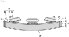
- Fig. 1 is a diagram (cross-sectional view) schematically representing an example of an element-mounted board of the present embodiment.
- the element-mounted board of Fig. 1 is provided with a heat-dissipating plate 1 and electronic elements 11 mounted on one surface side of the heat-dissipating plate 1.
- aluminum or magnesium-containing metal layers 3 are formed on the front and back surfaces of a flat plate-shaped metal-silicon carbide complex 2 (also referred to below as the complex 2) including aluminum or magnesium.
- the surface on the side on which the electronic elements 11 are mounted is a main surface 3A and the other surface is a main surface 3B.
- the heat-dissipating plate 1 has a plurality of through holes 5 in the outer peripheral portion thereof. More specifically, as described below, in a case where the heat-dissipating plate 1 is substantially rectangular, the through holes 5 are preferably provided at least at the four corners of the heat-dissipating plate 1.
- the through holes 5 are used when bonding the heat-dissipating plate 1 to other heat-dissipating components (for example, heat-dissipating fins, and the like) with screws or the like.
- the electronic element 11 includes at least a ceramic plate 12.
- the electronic element 11 has a structure in which the ceramic plate 12 is interposed between two metal layers 13.
- the electronic element 11 is mounted on the main surface 3A side of the heat-dissipating plate 1 by, for example, soldering with solder 14.
- soldering with solder 14.
- the flatness of the main surface 3B (that is, the surface on the opposite side to the surface on which the electronic elements 11 are mounted) is 50 ⁇ m to 600 ⁇ m, preferably 100 ⁇ m to 500 ⁇ m, and more preferably 150 um to 450 um.
- the flatness of the main surface 3B being an appropriate numerical value makes the bonding property between the main surface 3B and other heat-dissipating members favorable when the element-mounted board is bonded with other heat-dissipating members and makes it possible to obtain an excellent heat dissipation performance.
- Flatness is defined as the distance between two parallel planes in a case where the distance between the two parallel planes is the smallest when a flat shape is interposed between two geometrically parallel planes (refer to JIS B 0621).
- An example of a flatness measuring apparatus is the VR-3000 apparatus manufactured by Keyence Corporation.
- the main surface 3B (the surface of the heat-dissipating plate 1 on the opposite side to the surface on which the electronic element 11 is mounted) is curved to be convex in the direction of the opposite side to the main surface 3A. Due to this, when the heat-dissipating plate 1 is fixed to other heat-dissipating members (heat-dissipating fins, and the like) with fixing members such as screws, it is possible to easily make the bonding surface "flat” and to further improve the bonding property (adhesion) between the heat-dissipating plate 1 and the heat-dissipating fins and the like.
- the heat-dissipating plate 1 is substantially rectangular. In other words, when the heat-dissipating plate 1 is viewed from the top surface with one of the main surfaces of the heat-dissipating plate 1 as the top surface, the shape of the heat-dissipating plate 1 is substantially rectangular.
- substantially rectangular means that at least one of the four corners of the heat-dissipating plate 1 may be processed into a rounded shape instead of a right-angled shape (naturally, the four corners may be right-angled shapes).
- the vertical and horizontal lengths of the heat-dissipating plate 1 are from 40 mm ⁇ 90 mm to 250 mm ⁇ 140 mm approximately, as an example.
- the thickness of the heat-dissipating plate 1 is 2 mm or more and 6 mm or less and preferably 3 mm or more and 5 mm or less as an example. In a case where the thickness of the heat-dissipating plate 1 is not uniform, at least the thickness at the center of gravity portion of the heat-dissipating plate 1 is preferably in the range described above.
- the thickness of the metal layer 3 is, for example, approximately 50 um to 300 um for the top and bottom together.
- the heat-dissipating plate 1 is substantially rectangular, the length of the long side of the rectangle is a and the length of the short side is b, and the main surface 3B is curved to be convex in the direction of the opposite side to the main surface 3A may be considered.
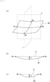
- Fig. 2(a) is a diagram for illustrating the form of the main surface 3B. To paraphrase, the diagram clearly shows only the main surface 3B of the heat-dissipating plate 1 in the element-mounted board of the present embodiment.
- Fig. 2(b) is a cross-sectional view when the main surface 3B is cut at the cross-section ⁇ in Fig. 2(a)
- Fig. 2(c) is a cross-sectional view when the main surface 3B is cut at the cross-section ⁇ in Fig. 2(a) .
- the straight line connecting the midpoints of the two short sides of the main surface 3B (shown by M 1 and M 3 in the diagram) is denoted by l 1
- the straight line connecting the midpoints of the two long sides of the main surface 3B (shown by M 2 and M 4 in the diagram) is denoted by l 2 .
- the maximum distance between a point on the curve formed by the main surface 3B and l 1 in the cross-section is denoted by h 1 .
- the maximum distance between the point on the curve formed by the main surface 3B and l 2 in the cross-section is denoted by h 2 .
- the element-mounted board is designed such that h 1 /a > h 2 /b.
- the value of (h 1 /a)/(h 2 /b) is 1.07 or more and 1.9 or less and preferably 1.07 or more and 1.6 or less.
- h 1 /a means "curvature per unit length in the long side direction" in the heat-dissipating plate 1.
- h 2 /b means "curvature per unit length in the short side direction" in the heat-dissipating plate 1.
- the rectangular shape (oblong shape) of the heat-dissipating plate 1 is more easily deformed (easily bent) in the long side direction than in the short side direction.
- the "degree of curvature" in the long side direction larger than that in the short side direction, it is considered that it is possible to bond the heat-dissipating plate 1 more snugly when bonding to other heat-dissipating components and to obtain an effect of further improving the heat dissipation property, improving the reliability, and the like.
- An arithmetic mean roughness Ra (referred to below as “surface roughness Ra") of the portion in the main surface 3A of the heat-dissipating plate 1 on which the electronic element 11 is not mounted (the portion where the main surface 3A is exposed) is preferably 0.2 um to 2.0 um and more preferably 0.5 um to 1.6 um.
- the electronic element 11 is mounted on the heat-dissipating plate 1 by soldering, for example, with the solder 14. It is considered that the value of the surface roughness Ra being appropriate increases the wettability of the solder and, as a result, it is possible to improve the bonding strength between the heat-dissipating plate 1 and the electronic element 11.
- the roughness (surface roughness Ra) of the main surface 3A being appropriate creates a kind of "play" between the heat-dissipating plate 1 and the electronic element 11. Due to this, it is also considered that the deterioration of the bonding property is suppressed even in the presence of external forces, heat cycles, distortion when connecting the element-mounted board to other heat-dissipating components, and the like.
- a plating layer may be present on the uppermost surface of the heat-dissipating plate 1. Due to this, for example, it is possible to further improve the bonding property with the electronic element 11 (specifically, soldering with the electronic elements 11 is easier). It is possible for the plating layer to be, for example, Ni plating. It is possible to set the thickness of the plating layer to approximately 10 um per layer and approximately 20 ⁇ m for the top and bottom combined.
- the electronic element 11 may be, for example, a power semiconductor element. Although a large amount of heat may be released from the electronic element 11, which is a power semiconductor element, the heat may be efficiently exhausted by appropriately bonding the element-mounted board of the present embodiment to other heat-dissipating members (heat-dissipating fins or the like).
- the electronic element 11 includes at least the ceramic plate 12.
- the electronic element 11 typically includes a metal layer 13.
- the material of the ceramic plate 12 is not particularly limited as long as it is a ceramic material.
- the material it is possible for the material to be a nitride ceramic such as silicon nitride and aluminum nitride, an oxide ceramic such as aluminum oxide and zirconium oxide, a carbide ceramic such as silicon carbide, a boride ceramic such as lanthanum boride, and the like.
- a nitride ceramic such as silicon nitride and aluminum nitride
- an oxide ceramic such as aluminum oxide and zirconium oxide
- a carbide ceramic such as silicon carbide
- a boride ceramic such as lanthanum boride
- aluminum nitride, silicon nitride, and aluminum oxide are preferable from the viewpoint of insulation properties, strength of the bonding property to the metal layer 13, mechanical strength, and the like.
- the metal layer 13 is preferably formed of copper, copper alloys, aluminum, and aluminum alloys from the viewpoint of electrical conductivity, thermal conductivity, and the like.
- the metal layer 13 it is possible for the metal layer 13 to be formed of pure copper (C1020 or C1011 material), an oxygen-free copper sheet, and the like.
- a part of the metal layer 13 may be removed by etching or the like to form a circuit pattern.
- the brazing material is preferably a mixture of Ag powder, Cu powder, or the like. From the viewpoint of moderating the melting temperature and the like, when the total of the Ag powder and Cu powder is 100 parts by mass, the Ag powder is preferably 75 parts by mass or more and 98 parts by mass or less and the Cu powder is preferably 2 parts by mass or more and 25 parts by mass or less.
- the brazing material may include Sn or In for the purpose of improving wettability with the ceramic plate or the like.
- the blending amount of these components is preferably 0.4 parts by mass or more and 3.5 parts by mass or less.
- the brazing material preferably includes active metals from the viewpoint of increasing reactivity with the ceramic plate and the like.
- active metals include titanium, zirconium, hafnium, niobium, and the like. It is preferable to include titanium from the viewpoint of enabling high reactivity with aluminum nitride substrates and silicon nitride substrates and an extremely high bonding strength.
- the added amount of the active metal is preferably 1.5 parts by mass or more and 5.0 parts by mass or less with respect to a total of 100 parts by mass of Ag powder, Cu powder, Sn powder, or In powder.
- brazing material by mixing the metal powder as described above with an organic solvent or binder as necessary.
- an organic solvent or binder for the mixing, it is possible to use a mortar machine, a revolving or orbital mixer, a planetary mixer, three rolls, and the like. Due to this, it is possible to obtain, for example, a paste-like brazing material.
- the organic solvents able to be used here are not particularly limited. Examples thereof include methyl cellusolve, ethyl cellusolve, isophorone, toluene, ethyl acetate, terpineol, diethylene glycol monobutyl ether, texanol, and the like.
- the binders able to be used here are not particularly limited. Examples thereof include polymer compounds such as polyisobutyl methacrylate, ethyl cellulose, methyl cellulose, acrylic resins, and methacrylic resins.
- the method for coating the brazing material paste on the ceramic plate in (1) described above is not particularly limited. Examples thereof include a roll coater method, a screen-printing method, a transfer method, and the like.
- the screen-printing method is preferable in terms of easy uniform coating.
- the process in a vacuum or in an inert atmosphere such as nitrogen or argon, for example, at a temperature of 770°C or higher and 830°C or lower for a time of 10 minutes or more to 60 minutes.
- the design concept of the element-mounted board of the present embodiment is to improve the heat dissipation property by integrally forming the heat-dissipating plate 1 and the electronic element 11, instead of just the heat-dissipating plate 1 alone.
- the difference between ⁇ 1 and ⁇ 2 is 5.0 ppm K -1 or less.
- the electronic element 11 when the element-mounted board is viewed from the top surface with the side of the main surface 3A of the heat-dissipating plate 1 as the top surface, the electronic element 11 preferably covers 10% to 80% of the area of the heat-dissipating plate 1 and more preferably 15% to 70%.
- the flatness of the main surface 3B is set to 50 um to 600 um, or the values of h 1 /a, h 2 /b, and the like are appropriately designed such that it is possible to obtain a favorable heat dissipation property while reducing the generation of unintended distortion, thermal stress, and the like to a good level.
- the type of the solder 14 is not particularly limited and, for example, it is possible to use lead-tin eutectic solder or lead-free solder. It is possible to set the thickness of the solder coating to be 0.1 mm to 0.2 mm, for example.
- the reflow conditions are not particularly limited and may be appropriately set according to the melting temperature or the like of the solder 14; however, typically, it is possible to set the conditions to 250°C to 350°C for approximately 5 minutes to 30 minutes. By ensuring that the temperature is not excessively high/time is not excessively long, it is possible to suppress unintended changes in flatness, and the like.
- a heat-dissipating plate on which metal layers are provided on both the front and back surfaces of a flat plate-shaped metal-silicon carbide complex by (i) a step of forming a silicon carbide powder into a flat plate-shape to carry out sintering and obtain a flat plate-shaped molded body (preform) and (ii) a step of impregnating the molded body (preform) with a metal.
- the raw silicon carbide powder (preferably one or two or more silicon carbide particles with an average particle diameter of 1 um to 300 ⁇ m) is made into a flat plate-shape by a suitable method.
- the method forming a flat plate-shape it is possible to appropriately apply known methods. For example, it is possible to use a dry press method, a wet press method, an extrusion molding method, an injection method, a casting method, a method of punching out after sheet forming, and the like.
- inorganic or organic binders may be appropriately added to develop strength such that abnormalities such as cracking are not generated during the metal impregnation.
- Silica sol is preferable as a binder since it is easy to obtain high-strength molded bodies.
- the addition of a binder with a volume ratio of 20 or less with respect to 100 silicon carbide as solid content is preferable for the reason of improved relative density.
- the flat plate obtained as described above is usually sintered after a drying, heating, and degreasing process, although this varies depending on the manufacturing conditions. Due to this, it is possible to obtain a molded body (also called a preform) having sufficient strength.
- the sintering conditions are preferably a temperature of 700°C or higher in an inert atmosphere or in air.
- the silicon carbide may be oxidized and the thermal conductivity of the obtained complex may decrease.
- the relative density of the preform obtained by sintering is preferably 55% to 75%.
- the thermal expansion coefficient of the heat-dissipating plate 1 is easily designed to be approximately 6 ppm/K to 10 ppm/K.
- the relative density is defined as the volume ratio of silicon carbide in the volume of the silicon carbide molded body (preform) having voids before impregnation with metal.
- silicon carbide powders of different particle sizes are preferably blended at the stage of obtaining the flat plate before sintering.
- examples thereof include using a mixture of powder with an average grain size of 100 ⁇ m and powder with an average grain size of 10 ⁇ m or finer, or powder in which powder with an average grain size of 60 ⁇ m and powder with an average grain size of 10 ⁇ m or finer are mixed.
- a part of the preform may be machined before the obtained preform is impregnated with metal.
- At least one surface of the preform may be processed by a cutting and grinding tool such as a lathe so as to have a convex curved shape toward the outside of the preform.
- a cutting and grinding tool such as a lathe
- step (ii) described above metal impregnation
- molten metal forging method or die-casting method it is possible to adopt a so-called molten metal forging method or die-casting method to impregnate the preform obtained by sintering with metal.
- the preform is impregnated with a metal including aluminum or magnesium and it is possible to produce a metal-silicon carbide complex provided with a complex part including silicon carbide and metal and a surface metal layer on the outer surface of the complex part.
- Examples of method for obtaining a metal-silicon carbide complex by impregnating the metal (alloy) including aluminum or magnesium into the preform include the following method.
- One or more fibers, spherical particles, and crushed-form particles formed of alumina or silica are arranged in direct contact with both surfaces of the preform and interposed between release plates to form a single block.
- the block is then preheated at 500°C or higher and 650°C or lower and then one or two or more are arranged in highpressure containers. Thereafter, as soon as possible to prevent the temperature of the block from dropping, molten metal including aluminum or magnesium is pressed at a pressure of 30 MPa or higher to impregnate the metal into the voids of the preform.
- a metal-silicon carbide complex provided with a complex part including silicon carbide and metal and a surface metal layer on the outer surface of the complex part is obtained.
- the preform is set in a mold having a cavity in the shape of the product, the mold is tightened, and then metal is injected therein at high speed to obtain the metal-silicon carbide complex.
- a metal layer on the surface of the metal-silicon carbide complex by devising the form of the concave mold and/or convex mold, more specifically, by devising the provision of a "gap", which corresponds to a metal layer, between the mold and the preform (that is, as shown in Fig. 1 , it is possible to obtain the heat-dissipating plate 1 with the metal layer 3 formed on the front and back surfaces of the complex 2).
- the composition of the metal impregnated in the complex and the composition of the metal forming the metal layer are basically the same.
- the metal to be impregnated is not particularly limited as long as it includes aluminum or magnesium.
- a metal with aluminum or magnesium as the main component is preferable and a metal with aluminum as the main component is more preferable.
- the metal to be impregnated may include other elements other than aluminum or magnesium.
- the metal to be impregnated may have aluminum as a main component and contain 0.1% by mass or more and 1.5% by mass or less of magnesium and 0.1% by mass or more and 18% by mass or less of silicon.
- the alloying of silicon and magnesium with aluminum has the advantage that the melting point of the alloy is decreased and the viscosity of the molten metal at high temperatures is decreased and it is easier to obtain a dense complex in high temperature casting or the like.
- An annealing process may be performed for the purpose of removing distortions created during impregnation or the like.
- An annealing process for the purpose of removing distortions is preferably performed at a temperature of 400°C or higher and 550°C or lower for 10 minutes or more.
- the annealing temperature is 400°C or higher, the distortion inside the heat-dissipating plate 1 is sufficiently eliminated, making it possible to suppress the curvature from changing significantly in the annealing process step after machining.
- the annealing temperature is 550°C or lower, it is possible to prevent melting of the metal (for example, aluminum alloy) used in the impregnation.
- the annealing time is 10 minutes or more, the distortion inside the heat-dissipating plate 1 is sufficiently eliminated and it is possible to suppress the curvature from changing significantly during the annealing process step of removing the processing distortion after machining.
- the heat-dissipating plate 1 is interposed between a press convex die 100 and a press concave die 110 and heated and pressed (pressed while being heated). Due to this, it is possible to adjust the flatness of the main surface of the heat-dissipating plate 1.
- the press convex die 100 and the press concave die 110 are shaped and processed such that a predetermined curvature is imparted to the heat-dissipating plate 1.
- the form of the convex portion of the press convex die 100 and the form of the concave portion of the press concave die 110 are approximately the same. In other words, typically, in a case where the press convex die 100 and the press concave die 110 are overlaid without interposing the heat-dissipating plate 1 therebetween, it is almost impossible to have space between the press convex die 100 and the press concave die 110.
- the material of the press convex die 100 and the press concave die 110 is not particularly limited other than being substantially non-deforming under the temperature and pressure conditions described below. Specifically, ceramics such as carbon and boron nitride and metal materials such as cemented carbide and stainless steel are preferably used.
- the heating temperature during heating and pressing is not particularly limited as long as it is possible to obtain the heat-dissipating plate 1 imparted with appropriate curvature.
- the heating temperature is preferably as high as possible in a range where the metal in the heat-dissipating plate 1 does not melt.
- the temperature is preferably 450°C or higher and 550°C or lower.
- the pressure during heating and pressing is not particularly limited as long as it is possible to obtain the heat-dissipating plate 1 imparted with an appropriate curvature.
- the pressure may be appropriately adjusted according to the thickness of the heat-dissipating plate 1, the heating temperature, and the like.
- the pressure is preferably 10 kPa or more and more preferably 30 kPa or more and 250 kPa or less.
- the time of the heating and pressing is also not particularly limited.
- the time during which the temperature of the heat-dissipating plate 1 itself is 450°C or more is preferably 30 seconds or more and more preferably 30 seconds or more and 300 seconds or less.
- the flatness adjustment may be performed by machining (grinding, cutting, or the like) at least one surface (the surface which is the main surface 3B when made into an element-mounted board) of the heat-dissipating plate 1 obtained as described above.
- machining grinding, cutting, or the like
- the warpage decreases by approximately 150 um in the long side direction and approximately 6 um in the short side direction.
- both heating and pressing and machining may be performed.
- the steps for manufacturing the heat-dissipating plate may include other steps not described above.
- the steps for manufacturing the heat-dissipating plate may include a step of providing holes for screw fastening. Specifically, it is possible to provide holes for screw fastening for bonding with other heat-dissipating components by machining or the like.
- the step of providing holes for screw fastening may be performed at any stage, but it is particularly preferably performed before machining in a case where machining is carried out when adjusting the flatness of the heat-dissipating plate. In this manner, it is also possible to use the provided holes for fixing to a lathe or the like.
- the steps for manufacturing the heat-dissipating plate may include a step of polishing one surface or both surfaces of the heat-dissipating plate as appropriate. Due to this, for example, it is possible to adjust the arithmetic mean roughness Ra of the surface of the heat-dissipating plate.
- the steps for manufacturing the heat-dissipating plate may include a step of providing a plating layer on the uppermost surface of the heat-dissipating plate.
- the significance and the like of providing a plating layer is as described above.
- an element-mounted board by (i) first, coating solder paste in paste form by adding flux to the surface of the heat-dissipating plate, for which the flatness or the like was adjusted as described above, (ii) installing an electronic element (for example, a ceramic circuit substrate) on the coated solder paste, and (iii) then melting the solder by reflowing.
- This bonding typically causes some change in the flatness of one surface of the heat-dissipating plate (the main surface 3B in Fig. 1 ) and the flatness becomes 50 ⁇ m to 600 um.
- the conditions for the reflowing described above are not particularly limited and may be set appropriately according to the melting temperature or the like of the solder and, typically, it is possible to set the temperature to be 250°C to 350°C for approximately 5 minutes to 30 minutes. By ensuring that the temperature is not excessively high and the time is not excessively long, it is possible to suppress unintended changes in flatness and the like.
- the obtained mixture was introduced into a mold and press-formed at a pressure of 10 MPa. Due to this, a flat plate-shaped molded body with dimensions of 185 mm ⁇ 135 mm ⁇ 5.5 mm was obtained.
- the obtained molded body was sintered at a temperature of 900°C for 2 hours in air to obtain a porous silicon carbide body with a relative density (bulk density) of 65% by volume.
- Alumina fibers manufactured by Tanaka Paper Industries Co., Ltd., 97% purity, sheet form
- both surfaces were interposed between carbon coated stainless steel plates with dimensions of 210 mm ⁇ 160 mm ⁇ 0.8 mm to laminate 30 sheets.
- steel plates of 6 mm thickness were arranged on both sides, connected with six M10 bolts, and tightened with a torque wrench such that the tightening torque in the surface direction was 3 Nm to make a single block.
- the integrated block was then preheated to 620°C in an electric furnace and then squeezed in a preheated press die with an inner diameter of 400 mm ⁇ .
- Molten metal of an aluminum alloy containing 12% by mass of silicon and 1.0% by mass of magnesium was poured into the press die and then pressed at a pressure of 100 MPa for 20 minutes. Due to this, the aluminum alloy was impregnated in the porous silicon carbide body.
- the result was cooled to 25°C and then cut along the shape of the release plate using a wet band saw and the interposed stainless-steel plate was peeled off. Furthermore, an annealing process was then performed at a temperature of 500°C for 3 hours to remove distortion during impregnation.
- the outer circumference of the obtained aluminum-silicon carbide complex was processed on an NC lathe to a size of 190 mm ⁇ 140 mm in length and width. Thereafter, through holes with a diameter of 7 mm were processed at 8 locations around the outer edge portion and countersunk holes with a diameter of ⁇ 10-4 mm were processed at 4 locations.
- the aluminum-silicon carbide complex was cleaned by a blasting process with alumina abrasive grains under conditions of a pressure of 0.4 MPa and a transfer speed of 1.0 m/min and then electroless Ni-P and Ni-B plating was performed. Due to this, plating layers with a thickness of 8 um (Ni-P: 6 um, Ni-B: 2 ⁇ m) were formed on the complex surface.
- heat-dissipating plate heat-dissipating member
- the material of the ceramic plate, linear expansion coefficient, material of the copper layer, and overall size and thickness are as follows.
- the material it is possible for the material to be a nitride ceramic such as silicon nitride and aluminum nitride, an oxide ceramic such as aluminum oxide and zirconium oxide, a carbide ceramic such as silicon carbide, a boride ceramic such as lanthanum boride, and the like.
- a nitride ceramic such as silicon nitride and aluminum nitride
- an oxide ceramic such as aluminum oxide and zirconium oxide
- a carbide ceramic such as silicon carbide
- a boride ceramic such as lanthanum boride
- aluminum nitride, silicon nitride, and aluminum oxide are preferable from the viewpoint of insulation properties, bonding strength to the metal layer 13, mechanical strength, and the like.
- solder composition soldering conditions, thickness, and area covered by the substrate used for soldering the heat-dissipating plate and electronic element are as follows.
- the flatness of the main surface 3B on the side where the electronic element 11 was not mounted was measured using a VR-3000 apparatus manufactured by Keyence Corporation to obtain a flatness f.
- a range of 190 mm ⁇ 100 mm was measured such that the center of the main surface 3B when viewed from the top surface (geometric center of gravity) and the center of the observation field of view of the measuring apparatus were aligned.
- Table 1 shows the results of the measurements of nine of the heat-dissipating plates 1 of the Examples (Examples 1 to 9).
- the flatness f was 363.7 um on average, with a maximum value of 480 ⁇ m, a minimum value of 246 um, and a standard deviation of 77.3.
- h 1 and h 2 were determined by analyzing the data.
- h 1 and h 2 were determined before and after mounting the electronic element 11 and the degree of change before and after mounting was confirmed.
- Table 1 shows (h 1 /a)/(h 2 /b) for nine of the heat-dissipating plates 1 as Examples (Examples 1 to 9).
- (h 1 /a)/(h 2 /b) was a minimum of 1.27 and a maximum of 1.78 and was included in the range of 1 or more and 1.9 or less as shown in the embodiment.
- Table 2 shows the change in the warpage before and after mounting the electronic element 11 for the three of the heat-dissipating plates 1 as Examples (Examples 10 to 12).
- the warpage decreases by approximately 150 um in the long side direction and approximately 6 um in the short side direction.
- the surface roughness Ra of the portion (the exposed portion of the main surface 3A) of the main surface 3A where the electronic element 11 is not mounted was measured with a measuring apparatus Surftest SJ-310 manufactured by Mitutoyo in accordance with ISO 4287-1997.
- the surface roughness Ra had an average of 1.02 um, a maximum value of 1.52, a minimum value of 0.84, and a standard deviation of 0.11.
- the heat-dissipating plates 1 of Examples 1 to 9 shown in Table 1 were bonded to a heat-dissipating fin by screws and, when the adhesiveness, heat dissipation property, and the like between the heat-dissipating plates 1 and the heat-dissipating fins were evaluated, the adhesiveness and the heat dissipation property were favorable.
- Example 1 Comparative Example
- the heat-dissipating plate when fixed to a Cu plate or an Al plate by screw fastening, the heat-dissipating plate became M-shaped and gaps were created between the Cu plate and the Al plate.
- the case covering the upper portion did not fit.
- Example 1 f h 1 h 1 /a h 2 h 2 /b (h 1 /a)/(h 2 /b)
- Example 1 286 172 0.000917 84 0.000611 1.502
- Example 2 294 165 0.000880 95 0.000691 1.274
- Example 3 246 144 0.000768 78 0.000567 1.354
- Example 4 326 202 0.001077 107 0.000778 1.384
- Example 5 480 217 0.001157 118 0.000858 1.349
- Example 6 417 210 0.001120 109 0.000793 1.413
- Example 7 403 257 0.001371 114 0.000829 1.653
- Example 8 415 285 0.001520 119 0.000865 1.756
- Example 9 397 275 0.001467 136 0.000989 1.483 a 187.5 mm b 137.5 mm
Landscapes
- Physics & Mathematics (AREA)
- Thermal Sciences (AREA)
- Engineering & Computer Science (AREA)
- Microelectronics & Electronic Packaging (AREA)
- Cooling Or The Like Of Semiconductors Or Solid State Devices (AREA)
Claims (5)
- Elementmontierte Platte, umfassend:eine im Wesentlichen rechteckige Wärmeableitplatte (1), bei der aluminium- oder magnesiumhaltige Metallschichten (3) auf sowohl der vorderseitigen als auch der rückseitigen Oberfläche eines flachen plattenförmigen Metall-Siliciumcarbid-Komplexes (2), der Aluminium oder Magnesium aufweist, ausgebildet sind; undein elektronisches Element (11), das eine Keramikplatte (12) aufweist, die auf einer Oberfläche (3A) der Wärmeableitplatte (1) montiert ist,wobei in einem Zustand, in dem das elektronische Element (11) auf der einen Oberfläche (3A) montiert ist,eine Planheit der anderen Oberfläche (3B) der Wärmeableitplatte (1) 600 µm oder weniger beträgt undwenn eine Länge einer langen Seite des Rechtecks mit a bezeichnet wird und eine Länge einer kurzen Seite des Rechtecks mit b bezeichnet wird,eine gerade Linie, die jeden Mittelpunkt (M1, M3) von zwei kurzen Seiten der anderen Oberfläche (3B) verbindet, l1 ist und eine gerade Linie, die jeden Mittelpunkt (M2, M4) von zwei langen Seiten der anderen Oberfläche (3B) verbindet, l2 ist,ein maximaler Abstand zwischen einem Punkt auf einer durch die andere Oberfläche (3B) ausgebildeten Kurve und l1 h1 ist, wenn die Wärmeableitplatte (1) im Querschnitt in einer Querschnittsansicht, die l1 aufweist und im Wesentlichen orthogonal zu der anderen Oberfläche (3B) ist, betrachtet wird, undein maximaler Abstand zwischen einem Punkt auf einer durch die andere Oberfläche (3B) ausgebildeten Kurve und l2 h2 ist, wenn die Wärmeableitplatte (1) im Querschnitt in einer Querschnittsansicht, die l2 aufweist und im Wesentlichen orthogonal zu der anderen Oberfläche (3B) ist, betrachtet wird,
 wobei (h1/a)/(h2/b) 1,07 oder mehr und 1,9 oder weniger ist.
 - Elementmontierte Platte nach Anspruch 1,
wobei, wenn ein Wärmeausdehnungskoeffizient der Wärmeableitplatte (1) zwischen Raumtemperatur und 400 °C α1 ist und ein Wärmeausdehnungskoeffizient der Keramikplatte (12) zwischen Raumtemperatur und 400 °C α2 ist, eine Differenz zwischen α1 und α2 5,0 ppm K-1 oder weniger beträgt. - Elementmontierte Platte nach einem der Ansprüche 1 oder 2,
wobei eine arithmetische mittlere Rauigkeit Ra eines Abschnitts der einen Oberfläche (3A) der Wärmeableitplatte (1), auf dem das elektronische Element (11) nicht montiert ist, 0,2 µm bis 2,0 µm beträgt. - Elementmontierte Platte nach einem der Ansprüche 1 bis 3,
wobei, wenn die elementmontierte Platte von einer oberen Oberfläche, mit der einen Oberfläche (3A) der Wärmeableitplatte (1) als die obere Oberfläche, betrachtet wird, 10 % bis 80 % einer Fläche der Wärmeableitplatte (1) mit dem elektronischen Element (11) bedeckt sind. - Verfahren zur Herstellung der elementmontierten Platte nach einem der Ansprüche 1 bis 4, wobei das Verfahren Folgendes umfasst:einen Fertigungsschritt zum Fertigen einer Wärmeableitplatte (1), bei der eine aluminium- oder magnesiumhaltige Metallschicht (3) auf sowohl der vorderseitigen als auch der rückseitigen Oberfläche eines flachen plattenförmigen Metall-Siliciumcarbid-Komplexes (2), der Aluminium oder Magnesium aufweist, ausgebildet wird;einen Planheitsanpassungsschritt zum Anpassen einer Planheit mindestens einer Oberfläche (3B) der Wärmeableitplatte (1); undeinen Montageschritt zum Montieren eines elektronischen Elements (11), das eine Keramikplatte (12) aufweist, auf einer Oberfläche (3A) auf einer Seite, die der einen Oberfläche (3B) der Wärmeableitplatte (1) gegenüberliegt.
Applications Claiming Priority (2)
| Application Number | Priority Date | Filing Date | Title |
|---|---|---|---|
| JP2020063126 | 2020-03-31 | ||
| PCT/JP2021/009761 WO2021200011A1 (ja) | 2020-03-31 | 2021-03-11 | 素子搭載基板、および素子搭載基板の製造方法 |
Publications (3)
| Publication Number | Publication Date |
|---|---|
| EP4131366A1 EP4131366A1 (de) | 2023-02-08 |
| EP4131366A4 EP4131366A4 (de) | 2023-09-06 |
| EP4131366B1 true EP4131366B1 (de) | 2024-08-14 |
Family
ID=77928844
Family Applications (1)
| Application Number | Title | Priority Date | Filing Date |
|---|---|---|---|
| EP21780084.6A Active EP4131366B1 (de) | 2020-03-31 | 2021-03-11 | Elementmontierte platte und verfahren zur herstellung der elementmontierten platte |
Country Status (5)
| Country | Link |
|---|---|
| US (1) | US12219739B2 (de) |
| EP (1) | EP4131366B1 (de) |
| JP (1) | JP7596363B2 (de) |
| CN (1) | CN115315804B (de) |
| WO (1) | WO2021200011A1 (de) |
Families Citing this family (2)
| Publication number | Priority date | Publication date | Assignee | Title |
|---|---|---|---|---|
| KR102580589B1 (ko) * | 2020-12-28 | 2023-09-20 | 주식회사 아모센스 | 전력반도체 모듈의 제조방법 및 이에 의해 제조된 전력반도체 모듈 |
| CN117956750B (zh) * | 2024-01-02 | 2025-02-11 | 华为技术有限公司 | 电子设备、均温板及其制备方法 |
Family Cites Families (11)
| Publication number | Priority date | Publication date | Assignee | Title |
|---|---|---|---|---|
| JPS468358B1 (de) | 1967-01-27 | 1971-03-02 | ||
| JP3468358B2 (ja) | 1998-11-12 | 2003-11-17 | 電気化学工業株式会社 | 炭化珪素質複合体及びその製造方法とそれを用いた放熱部品 |
| JP3907620B2 (ja) * | 2003-11-14 | 2007-04-18 | 電気化学工業株式会社 | セラミックス回路基板一体型アルミニウム−炭化珪素質複合体及びその製造方法 |
| WO2006030676A1 (ja) * | 2004-09-14 | 2006-03-23 | Denki Kagaku Kogyo Kabushiki Kaisha | アルミニウム-炭化珪素質複合体 |
| JP4191124B2 (ja) | 2004-10-25 | 2008-12-03 | 電気化学工業株式会社 | アルミニウム合金−セラミックス質複合体及びその製造方法 |
| JPWO2015115649A1 (ja) | 2014-02-03 | 2017-03-23 | デンカ株式会社 | 炭化珪素質複合体及びその製造方法並びにそれを用いた放熱部品 |
| CN106796925B (zh) | 2014-07-31 | 2019-09-24 | 电化株式会社 | 铝-碳化硅质复合体及其制造方法 |
| US10636723B2 (en) * | 2014-08-06 | 2020-04-28 | Denka Company Limited | Heat dissipation component and method for manufacturing same |
| US10640853B2 (en) | 2016-03-15 | 2020-05-05 | Denka Company Limited | Aluminum-diamond-based composite and heat dissipation component |
| JP7120622B2 (ja) | 2018-10-17 | 2022-08-17 | ホリゾン・インターナショナル株式会社 | ナイフ折り機及びその制御装置並びにナイフ折り機の制御方法 |
| JP6591113B1 (ja) * | 2019-06-05 | 2019-10-16 | デンカ株式会社 | 放熱部材およびその製造方法 |
-
2021
- 2021-03-11 JP JP2022511755A patent/JP7596363B2/ja active Active
- 2021-03-11 US US17/911,890 patent/US12219739B2/en active Active
- 2021-03-11 EP EP21780084.6A patent/EP4131366B1/de active Active
- 2021-03-11 WO PCT/JP2021/009761 patent/WO2021200011A1/ja not_active Ceased
- 2021-03-11 CN CN202180023373.9A patent/CN115315804B/zh active Active
Also Published As
| Publication number | Publication date |
|---|---|
| US12219739B2 (en) | 2025-02-04 |
| EP4131366A4 (de) | 2023-09-06 |
| CN115315804A (zh) | 2022-11-08 |
| US20230156966A1 (en) | 2023-05-18 |
| WO2021200011A1 (ja) | 2021-10-07 |
| JPWO2021200011A1 (de) | 2021-10-07 |
| JP7596363B2 (ja) | 2024-12-09 |
| CN115315804B (zh) | 2025-12-12 |
| EP4131366A1 (de) | 2023-02-08 |
Similar Documents
| Publication | Publication Date | Title |
|---|---|---|
| JP7219810B2 (ja) | 窒化珪素基板、窒化珪素-金属複合体、窒化珪素回路基板、及び、半導体パッケージ | |
| KR101344152B1 (ko) | 알루미늄-탄화규소질 복합체 및 그것을 사용한 방열 부품 | |
| CN101361184B (zh) | 铝-碳化硅复合体和使用该复合体的散热零件 | |
| JP5021636B2 (ja) | アルミニウム−炭化珪素質複合体及びその加工方法 | |
| TWI357788B (de) | ||
| EP3920215B1 (de) | Wärmeabführungselement und herstellungsverfahren dafür | |
| EP3885331B1 (de) | Keramik-kupferverbund, verfahren zur herstellung eines keramik-kupferverbundes, keramische leiterplatte und leistungsmodul | |
| US12120852B2 (en) | Composite material and heat dissipation part | |
| US12219739B2 (en) | Element-mounted board and method for manufacturing element-mounted board | |
| JP3907620B2 (ja) | セラミックス回路基板一体型アルミニウム−炭化珪素質複合体及びその製造方法 | |
| JP6591113B1 (ja) | 放熱部材およびその製造方法 | |
| EP4411810A1 (de) | Wärmeableitungselement | |
| JP7733530B2 (ja) | 放熱部材の製造方法 | |
| WO2024181224A1 (ja) | セラミックス板、包装体、セラミックス板の製造方法、モジュールおよび電気・電子製品 | |
| JP2026077977A (ja) | セラミックス板、包装体、セラミックス板の製造方法、モジュールおよび電気・電子製品 | |
| JP2012171838A (ja) | アルミニウム−炭化珪素質複合体の製造方法 | |
| JP2025154773A (ja) | 放熱部材および電子装置 |
Legal Events
| Date | Code | Title | Description |
|---|---|---|---|
| STAA | Information on the status of an ep patent application or granted ep patent |
Free format text: STATUS: THE INTERNATIONAL PUBLICATION HAS BEEN MADE |
|
| PUAI | Public reference made under article 153(3) epc to a published international application that has entered the european phase |
Free format text: ORIGINAL CODE: 0009012 |
|
| STAA | Information on the status of an ep patent application or granted ep patent |
Free format text: STATUS: REQUEST FOR EXAMINATION WAS MADE |
|
| 17P | Request for examination filed |
Effective date: 20221020 |
|
| AK | Designated contracting states |
Kind code of ref document: A1 Designated state(s): AL AT BE BG CH CY CZ DE DK EE ES FI FR GB GR HR HU IE IS IT LI LT LU LV MC MK MT NL NO PL PT RO RS SE SI SK SM TR |
|
| DAV | Request for validation of the european patent (deleted) | ||
| DAX | Request for extension of the european patent (deleted) | ||
| A4 | Supplementary search report drawn up and despatched |
Effective date: 20230807 |
|
| RIC1 | Information provided on ipc code assigned before grant |
Ipc: H01L 23/373 20060101ALI20230801BHEP Ipc: H01L 23/36 20060101AFI20230801BHEP |
|
| GRAP | Despatch of communication of intention to grant a patent |
Free format text: ORIGINAL CODE: EPIDOSNIGR1 |
|
| STAA | Information on the status of an ep patent application or granted ep patent |
Free format text: STATUS: GRANT OF PATENT IS INTENDED |
|
| INTG | Intention to grant announced |
Effective date: 20240314 |
|
| GRAS | Grant fee paid |
Free format text: ORIGINAL CODE: EPIDOSNIGR3 |
|
| GRAA | (expected) grant |
Free format text: ORIGINAL CODE: 0009210 |
|
| STAA | Information on the status of an ep patent application or granted ep patent |
Free format text: STATUS: THE PATENT HAS BEEN GRANTED |
|
| AK | Designated contracting states |
Kind code of ref document: B1 Designated state(s): AL AT BE BG CH CY CZ DE DK EE ES FI FR GB GR HR HU IE IS IT LI LT LU LV MC MK MT NL NO PL PT RO RS SE SI SK SM TR |
|
| REG | Reference to a national code |
Ref country code: GB Ref legal event code: FG4D |
|
| REG | Reference to a national code |
Ref country code: CH Ref legal event code: EP |
|
| REG | Reference to a national code |
Ref country code: DE Ref legal event code: R096 Ref document number: 602021017287 Country of ref document: DE |
|
| REG | Reference to a national code |
Ref country code: IE Ref legal event code: FG4D |
|
| P01 | Opt-out of the competence of the unified patent court (upc) registered |
Free format text: CASE NUMBER: APP_46554/2024 Effective date: 20240812 |
|
| REG | Reference to a national code |
Ref country code: LT Ref legal event code: MG9D |
|
| REG | Reference to a national code |
Ref country code: NL Ref legal event code: MP Effective date: 20240814 |
|
| PG25 | Lapsed in a contracting state [announced via postgrant information from national office to epo] |
Ref country code: NO Free format text: LAPSE BECAUSE OF FAILURE TO SUBMIT A TRANSLATION OF THE DESCRIPTION OR TO PAY THE FEE WITHIN THE PRESCRIBED TIME-LIMIT Effective date: 20241114 |
|
| REG | Reference to a national code |
Ref country code: AT Ref legal event code: MK05 Ref document number: 1714113 Country of ref document: AT Kind code of ref document: T Effective date: 20240814 |
|
| PG25 | Lapsed in a contracting state [announced via postgrant information from national office to epo] |
Ref country code: FI Free format text: LAPSE BECAUSE OF FAILURE TO SUBMIT A TRANSLATION OF THE DESCRIPTION OR TO PAY THE FEE WITHIN THE PRESCRIBED TIME-LIMIT Effective date: 20240814 Ref country code: NL Free format text: LAPSE BECAUSE OF FAILURE TO SUBMIT A TRANSLATION OF THE DESCRIPTION OR TO PAY THE FEE WITHIN THE PRESCRIBED TIME-LIMIT Effective date: 20240814 Ref country code: PL Free format text: LAPSE BECAUSE OF FAILURE TO SUBMIT A TRANSLATION OF THE DESCRIPTION OR TO PAY THE FEE WITHIN THE PRESCRIBED TIME-LIMIT Effective date: 20240814 Ref country code: GR Free format text: LAPSE BECAUSE OF FAILURE TO SUBMIT A TRANSLATION OF THE DESCRIPTION OR TO PAY THE FEE WITHIN THE PRESCRIBED TIME-LIMIT Effective date: 20241115 Ref country code: PT Free format text: LAPSE BECAUSE OF FAILURE TO SUBMIT A TRANSLATION OF THE DESCRIPTION OR TO PAY THE FEE WITHIN THE PRESCRIBED TIME-LIMIT Effective date: 20241216 |
|
| PG25 | Lapsed in a contracting state [announced via postgrant information from national office to epo] |
Ref country code: BG Free format text: LAPSE BECAUSE OF FAILURE TO SUBMIT A TRANSLATION OF THE DESCRIPTION OR TO PAY THE FEE WITHIN THE PRESCRIBED TIME-LIMIT Effective date: 20240814 |
|
| PG25 | Lapsed in a contracting state [announced via postgrant information from national office to epo] |
Ref country code: LV Free format text: LAPSE BECAUSE OF FAILURE TO SUBMIT A TRANSLATION OF THE DESCRIPTION OR TO PAY THE FEE WITHIN THE PRESCRIBED TIME-LIMIT Effective date: 20240814 |
|
| PG25 | Lapsed in a contracting state [announced via postgrant information from national office to epo] |
Ref country code: AT Free format text: LAPSE BECAUSE OF FAILURE TO SUBMIT A TRANSLATION OF THE DESCRIPTION OR TO PAY THE FEE WITHIN THE PRESCRIBED TIME-LIMIT Effective date: 20240814 Ref country code: IS Free format text: LAPSE BECAUSE OF FAILURE TO SUBMIT A TRANSLATION OF THE DESCRIPTION OR TO PAY THE FEE WITHIN THE PRESCRIBED TIME-LIMIT Effective date: 20241214 |
|
| PG25 | Lapsed in a contracting state [announced via postgrant information from national office to epo] |
Ref country code: HR Free format text: LAPSE BECAUSE OF FAILURE TO SUBMIT A TRANSLATION OF THE DESCRIPTION OR TO PAY THE FEE WITHIN THE PRESCRIBED TIME-LIMIT Effective date: 20240814 |
|
| PG25 | Lapsed in a contracting state [announced via postgrant information from national office to epo] |
Ref country code: ES Free format text: LAPSE BECAUSE OF FAILURE TO SUBMIT A TRANSLATION OF THE DESCRIPTION OR TO PAY THE FEE WITHIN THE PRESCRIBED TIME-LIMIT Effective date: 20240814 Ref country code: RS Free format text: LAPSE BECAUSE OF FAILURE TO SUBMIT A TRANSLATION OF THE DESCRIPTION OR TO PAY THE FEE WITHIN THE PRESCRIBED TIME-LIMIT Effective date: 20241114 |
|
| PG25 | Lapsed in a contracting state [announced via postgrant information from national office to epo] |
Ref country code: RS Free format text: LAPSE BECAUSE OF FAILURE TO SUBMIT A TRANSLATION OF THE DESCRIPTION OR TO PAY THE FEE WITHIN THE PRESCRIBED TIME-LIMIT Effective date: 20241114 Ref country code: PT Free format text: LAPSE BECAUSE OF FAILURE TO SUBMIT A TRANSLATION OF THE DESCRIPTION OR TO PAY THE FEE WITHIN THE PRESCRIBED TIME-LIMIT Effective date: 20241216 Ref country code: PL Free format text: LAPSE BECAUSE OF FAILURE TO SUBMIT A TRANSLATION OF THE DESCRIPTION OR TO PAY THE FEE WITHIN THE PRESCRIBED TIME-LIMIT Effective date: 20240814 Ref country code: NO Free format text: LAPSE BECAUSE OF FAILURE TO SUBMIT A TRANSLATION OF THE DESCRIPTION OR TO PAY THE FEE WITHIN THE PRESCRIBED TIME-LIMIT Effective date: 20241114 Ref country code: NL Free format text: LAPSE BECAUSE OF FAILURE TO SUBMIT A TRANSLATION OF THE DESCRIPTION OR TO PAY THE FEE WITHIN THE PRESCRIBED TIME-LIMIT Effective date: 20240814 Ref country code: LV Free format text: LAPSE BECAUSE OF FAILURE TO SUBMIT A TRANSLATION OF THE DESCRIPTION OR TO PAY THE FEE WITHIN THE PRESCRIBED TIME-LIMIT Effective date: 20240814 Ref country code: IS Free format text: LAPSE BECAUSE OF FAILURE TO SUBMIT A TRANSLATION OF THE DESCRIPTION OR TO PAY THE FEE WITHIN THE PRESCRIBED TIME-LIMIT Effective date: 20241214 Ref country code: HR Free format text: LAPSE BECAUSE OF FAILURE TO SUBMIT A TRANSLATION OF THE DESCRIPTION OR TO PAY THE FEE WITHIN THE PRESCRIBED TIME-LIMIT Effective date: 20240814 Ref country code: GR Free format text: LAPSE BECAUSE OF FAILURE TO SUBMIT A TRANSLATION OF THE DESCRIPTION OR TO PAY THE FEE WITHIN THE PRESCRIBED TIME-LIMIT Effective date: 20241115 Ref country code: FI Free format text: LAPSE BECAUSE OF FAILURE TO SUBMIT A TRANSLATION OF THE DESCRIPTION OR TO PAY THE FEE WITHIN THE PRESCRIBED TIME-LIMIT Effective date: 20240814 Ref country code: ES Free format text: LAPSE BECAUSE OF FAILURE TO SUBMIT A TRANSLATION OF THE DESCRIPTION OR TO PAY THE FEE WITHIN THE PRESCRIBED TIME-LIMIT Effective date: 20240814 Ref country code: BG Free format text: LAPSE BECAUSE OF FAILURE TO SUBMIT A TRANSLATION OF THE DESCRIPTION OR TO PAY THE FEE WITHIN THE PRESCRIBED TIME-LIMIT Effective date: 20240814 Ref country code: AT Free format text: LAPSE BECAUSE OF FAILURE TO SUBMIT A TRANSLATION OF THE DESCRIPTION OR TO PAY THE FEE WITHIN THE PRESCRIBED TIME-LIMIT Effective date: 20240814 |
|
| PGFP | Annual fee paid to national office [announced via postgrant information from national office to epo] |
Ref country code: DE Payment date: 20250128 Year of fee payment: 5 |
|
| PG25 | Lapsed in a contracting state [announced via postgrant information from national office to epo] |
Ref country code: DK Free format text: LAPSE BECAUSE OF FAILURE TO SUBMIT A TRANSLATION OF THE DESCRIPTION OR TO PAY THE FEE WITHIN THE PRESCRIBED TIME-LIMIT Effective date: 20240814 Ref country code: SM Free format text: LAPSE BECAUSE OF FAILURE TO SUBMIT A TRANSLATION OF THE DESCRIPTION OR TO PAY THE FEE WITHIN THE PRESCRIBED TIME-LIMIT Effective date: 20240814 Ref country code: RO Free format text: LAPSE BECAUSE OF FAILURE TO SUBMIT A TRANSLATION OF THE DESCRIPTION OR TO PAY THE FEE WITHIN THE PRESCRIBED TIME-LIMIT Effective date: 20240814 |
|
| PG25 | Lapsed in a contracting state [announced via postgrant information from national office to epo] |
Ref country code: EE Free format text: LAPSE BECAUSE OF FAILURE TO SUBMIT A TRANSLATION OF THE DESCRIPTION OR TO PAY THE FEE WITHIN THE PRESCRIBED TIME-LIMIT Effective date: 20240814 |
|
| PG25 | Lapsed in a contracting state [announced via postgrant information from national office to epo] |
Ref country code: CZ Free format text: LAPSE BECAUSE OF FAILURE TO SUBMIT A TRANSLATION OF THE DESCRIPTION OR TO PAY THE FEE WITHIN THE PRESCRIBED TIME-LIMIT Effective date: 20240814 |
|
| PG25 | Lapsed in a contracting state [announced via postgrant information from national office to epo] |
Ref country code: IT Free format text: LAPSE BECAUSE OF FAILURE TO SUBMIT A TRANSLATION OF THE DESCRIPTION OR TO PAY THE FEE WITHIN THE PRESCRIBED TIME-LIMIT Effective date: 20240814 Ref country code: SK Free format text: LAPSE BECAUSE OF FAILURE TO SUBMIT A TRANSLATION OF THE DESCRIPTION OR TO PAY THE FEE WITHIN THE PRESCRIBED TIME-LIMIT Effective date: 20240814 |
|
| REG | Reference to a national code |
Ref country code: DE Ref legal event code: R097 Ref document number: 602021017287 Country of ref document: DE |
|
| PLBE | No opposition filed within time limit |
Free format text: ORIGINAL CODE: 0009261 |
|
| STAA | Information on the status of an ep patent application or granted ep patent |
Free format text: STATUS: NO OPPOSITION FILED WITHIN TIME LIMIT |
|
| 26N | No opposition filed |
Effective date: 20250515 |
|
| PGFP | Annual fee paid to national office [announced via postgrant information from national office to epo] |
Ref country code: CH Payment date: 20250401 Year of fee payment: 5 |
|
| PG25 | Lapsed in a contracting state [announced via postgrant information from national office to epo] |
Ref country code: SE Free format text: LAPSE BECAUSE OF FAILURE TO SUBMIT A TRANSLATION OF THE DESCRIPTION OR TO PAY THE FEE WITHIN THE PRESCRIBED TIME-LIMIT Effective date: 20240814 |
|
| PG25 | Lapsed in a contracting state [announced via postgrant information from national office to epo] |
Ref country code: MC Free format text: LAPSE BECAUSE OF FAILURE TO SUBMIT A TRANSLATION OF THE DESCRIPTION OR TO PAY THE FEE WITHIN THE PRESCRIBED TIME-LIMIT Effective date: 20240814 |
|
| PG25 | Lapsed in a contracting state [announced via postgrant information from national office to epo] |
Ref country code: LU Free format text: LAPSE BECAUSE OF NON-PAYMENT OF DUE FEES Effective date: 20250311 |
|
| GBPC | Gb: european patent ceased through non-payment of renewal fee |
Effective date: 20250311 |
|
| REG | Reference to a national code |
Ref country code: DE Ref legal event code: R079 Ref document number: 602021017287 Country of ref document: DE Free format text: PREVIOUS MAIN CLASS: H01L0023360000 Ipc: H10W0040200000 |
|
| REG | Reference to a national code |
Ref country code: BE Ref legal event code: MM Effective date: 20250331 |
|
| PG25 | Lapsed in a contracting state [announced via postgrant information from national office to epo] |
Ref country code: GB Free format text: LAPSE BECAUSE OF NON-PAYMENT OF DUE FEES Effective date: 20250311 |
|
| PG25 | Lapsed in a contracting state [announced via postgrant information from national office to epo] |
Ref country code: FR Free format text: LAPSE BECAUSE OF NON-PAYMENT OF DUE FEES Effective date: 20250331 |
|
| PG25 | Lapsed in a contracting state [announced via postgrant information from national office to epo] |
Ref country code: BE Free format text: LAPSE BECAUSE OF NON-PAYMENT OF DUE FEES Effective date: 20250331 |
|
| PG25 | Lapsed in a contracting state [announced via postgrant information from national office to epo] |
Ref country code: IE Free format text: LAPSE BECAUSE OF NON-PAYMENT OF DUE FEES Effective date: 20250311 |