EP4131374A1 - Structure semi-conductrice et son procédé de fabrication - Google Patents
Structure semi-conductrice et son procédé de fabrication Download PDFInfo
- Publication number
- EP4131374A1 EP4131374A1 EP20931045.7A EP20931045A EP4131374A1 EP 4131374 A1 EP4131374 A1 EP 4131374A1 EP 20931045 A EP20931045 A EP 20931045A EP 4131374 A1 EP4131374 A1 EP 4131374A1
- Authority
- EP
- European Patent Office
- Prior art keywords
- connection pad
- sidewall
- wafer
- opening
- vertical
- Prior art date
- Legal status (The legal status is an assumption and is not a legal conclusion. Google has not performed a legal analysis and makes no representation as to the accuracy of the status listed.)
- Pending
Links
Images


Classifications
-
- H—ELECTRICITY
- H10—SEMICONDUCTOR DEVICES; ELECTRIC SOLID-STATE DEVICES NOT OTHERWISE PROVIDED FOR
- H10P—GENERIC PROCESSES OR APPARATUS FOR THE MANUFACTURE OR TREATMENT OF DEVICES COVERED BY CLASS H10
- H10P10/00—Bonding of wafers, substrates or parts of devices
- H10P10/12—Bonding of semiconductor wafers or semiconductor substrates to semiconductor wafers or semiconductor substrates
-
- H—ELECTRICITY
- H10—SEMICONDUCTOR DEVICES; ELECTRIC SOLID-STATE DEVICES NOT OTHERWISE PROVIDED FOR
- H10F—INORGANIC SEMICONDUCTOR DEVICES SENSITIVE TO INFRARED RADIATION, LIGHT, ELECTROMAGNETIC RADIATION OF SHORTER WAVELENGTH OR CORPUSCULAR RADIATION
- H10F39/00—Integrated devices, or assemblies of multiple devices, comprising at least one element covered by group H10F30/00, e.g. radiation detectors comprising photodiode arrays
- H10F39/011—Manufacture or treatment of image sensors covered by group H10F39/12
- H10F39/018—Manufacture or treatment of image sensors covered by group H10F39/12 of hybrid image sensors
-
- H—ELECTRICITY
- H10—SEMICONDUCTOR DEVICES; ELECTRIC SOLID-STATE DEVICES NOT OTHERWISE PROVIDED FOR
- H10F—INORGANIC SEMICONDUCTOR DEVICES SENSITIVE TO INFRARED RADIATION, LIGHT, ELECTROMAGNETIC RADIATION OF SHORTER WAVELENGTH OR CORPUSCULAR RADIATION
- H10F39/00—Integrated devices, or assemblies of multiple devices, comprising at least one element covered by group H10F30/00, e.g. radiation detectors comprising photodiode arrays
- H10F39/80—Constructional details of image sensors
- H10F39/809—Constructional details of image sensors of hybrid image sensors
-
- H—ELECTRICITY
- H10—SEMICONDUCTOR DEVICES; ELECTRIC SOLID-STATE DEVICES NOT OTHERWISE PROVIDED FOR
- H10W—GENERIC PACKAGES, INTERCONNECTIONS, CONNECTORS OR OTHER CONSTRUCTIONAL DETAILS OF DEVICES COVERED BY CLASS H10
- H10W20/00—Interconnections in chips, wafers or substrates
- H10W20/01—Manufacture or treatment
- H10W20/021—Manufacture or treatment of interconnections within wafers or substrates
- H10W20/023—Manufacture or treatment of interconnections within wafers or substrates the interconnections being through-semiconductor vias
- H10W20/0234—Manufacture or treatment of interconnections within wafers or substrates the interconnections being through-semiconductor vias comprising etching via holes that stop on pads or on electrodes
-
- H—ELECTRICITY
- H10—SEMICONDUCTOR DEVICES; ELECTRIC SOLID-STATE DEVICES NOT OTHERWISE PROVIDED FOR
- H10W—GENERIC PACKAGES, INTERCONNECTIONS, CONNECTORS OR OTHER CONSTRUCTIONAL DETAILS OF DEVICES COVERED BY CLASS H10
- H10W20/00—Interconnections in chips, wafers or substrates
- H10W20/01—Manufacture or treatment
- H10W20/021—Manufacture or treatment of interconnections within wafers or substrates
- H10W20/023—Manufacture or treatment of interconnections within wafers or substrates the interconnections being through-semiconductor vias
- H10W20/0238—Manufacture or treatment of interconnections within wafers or substrates the interconnections being through-semiconductor vias comprising etching via holes through pads or through electrodes
-
- H—ELECTRICITY
- H10—SEMICONDUCTOR DEVICES; ELECTRIC SOLID-STATE DEVICES NOT OTHERWISE PROVIDED FOR
- H10W—GENERIC PACKAGES, INTERCONNECTIONS, CONNECTORS OR OTHER CONSTRUCTIONAL DETAILS OF DEVICES COVERED BY CLASS H10
- H10W20/00—Interconnections in chips, wafers or substrates
- H10W20/01—Manufacture or treatment
- H10W20/021—Manufacture or treatment of interconnections within wafers or substrates
- H10W20/023—Manufacture or treatment of interconnections within wafers or substrates the interconnections being through-semiconductor vias
- H10W20/0242—Manufacture or treatment of interconnections within wafers or substrates the interconnections being through-semiconductor vias comprising etching via holes from the back sides of the chips, wafers or substrates
-
- H—ELECTRICITY
- H10—SEMICONDUCTOR DEVICES; ELECTRIC SOLID-STATE DEVICES NOT OTHERWISE PROVIDED FOR
- H10W—GENERIC PACKAGES, INTERCONNECTIONS, CONNECTORS OR OTHER CONSTRUCTIONAL DETAILS OF DEVICES COVERED BY CLASS H10
- H10W20/00—Interconnections in chips, wafers or substrates
- H10W20/01—Manufacture or treatment
- H10W20/021—Manufacture or treatment of interconnections within wafers or substrates
- H10W20/023—Manufacture or treatment of interconnections within wafers or substrates the interconnections being through-semiconductor vias
- H10W20/0253—Manufacture or treatment of interconnections within wafers or substrates the interconnections being through-semiconductor vias comprising forming the through-semiconductor vias after stacking of the chips, wafers or substrates
-
- H—ELECTRICITY
- H10—SEMICONDUCTOR DEVICES; ELECTRIC SOLID-STATE DEVICES NOT OTHERWISE PROVIDED FOR
- H10W—GENERIC PACKAGES, INTERCONNECTIONS, CONNECTORS OR OTHER CONSTRUCTIONAL DETAILS OF DEVICES COVERED BY CLASS H10
- H10W20/00—Interconnections in chips, wafers or substrates
- H10W20/20—Interconnections within wafers or substrates, e.g. through-silicon vias [TSV]
- H10W20/211—Through-semiconductor vias, e.g. TSVs
- H10W20/212—Top-view shapes or dispositions, e.g. top-view layouts of the vias
- H10W20/2125—Top-view shapes
-
- H—ELECTRICITY
- H10—SEMICONDUCTOR DEVICES; ELECTRIC SOLID-STATE DEVICES NOT OTHERWISE PROVIDED FOR
- H10W—GENERIC PACKAGES, INTERCONNECTIONS, CONNECTORS OR OTHER CONSTRUCTIONAL DETAILS OF DEVICES COVERED BY CLASS H10
- H10W20/00—Interconnections in chips, wafers or substrates
- H10W20/20—Interconnections within wafers or substrates, e.g. through-silicon vias [TSV]
- H10W20/211—Through-semiconductor vias, e.g. TSVs
- H10W20/213—Cross-sectional shapes or dispositions
- H10W20/2134—TSVs extending from the semiconductor wafer into back-end-of-line layers
-
- H—ELECTRICITY
- H10—SEMICONDUCTOR DEVICES; ELECTRIC SOLID-STATE DEVICES NOT OTHERWISE PROVIDED FOR
- H10W—GENERIC PACKAGES, INTERCONNECTIONS, CONNECTORS OR OTHER CONSTRUCTIONAL DETAILS OF DEVICES COVERED BY CLASS H10
- H10W20/00—Interconnections in chips, wafers or substrates
- H10W20/40—Interconnections external to wafers or substrates, e.g. back-end-of-line [BEOL] metallisations or vias connecting to gate electrodes
- H10W20/41—Interconnections external to wafers or substrates, e.g. back-end-of-line [BEOL] metallisations or vias connecting to gate electrodes characterised by their conductive parts
- H10W20/435—Cross-sectional shapes or dispositions of interconnections
-
- H—ELECTRICITY
- H10—SEMICONDUCTOR DEVICES; ELECTRIC SOLID-STATE DEVICES NOT OTHERWISE PROVIDED FOR
- H10W—GENERIC PACKAGES, INTERCONNECTIONS, CONNECTORS OR OTHER CONSTRUCTIONAL DETAILS OF DEVICES COVERED BY CLASS H10
- H10W90/00—Package configurations
-
- H—ELECTRICITY
- H10—SEMICONDUCTOR DEVICES; ELECTRIC SOLID-STATE DEVICES NOT OTHERWISE PROVIDED FOR
- H10F—INORGANIC SEMICONDUCTOR DEVICES SENSITIVE TO INFRARED RADIATION, LIGHT, ELECTROMAGNETIC RADIATION OF SHORTER WAVELENGTH OR CORPUSCULAR RADIATION
- H10F39/00—Integrated devices, or assemblies of multiple devices, comprising at least one element covered by group H10F30/00, e.g. radiation detectors comprising photodiode arrays
- H10F39/80—Constructional details of image sensors
- H10F39/811—Interconnections
-
- H—ELECTRICITY
- H10—SEMICONDUCTOR DEVICES; ELECTRIC SOLID-STATE DEVICES NOT OTHERWISE PROVIDED FOR
- H10W—GENERIC PACKAGES, INTERCONNECTIONS, CONNECTORS OR OTHER CONSTRUCTIONAL DETAILS OF DEVICES COVERED BY CLASS H10
- H10W20/00—Interconnections in chips, wafers or substrates
- H10W20/40—Interconnections external to wafers or substrates, e.g. back-end-of-line [BEOL] metallisations or vias connecting to gate electrodes
- H10W20/41—Interconnections external to wafers or substrates, e.g. back-end-of-line [BEOL] metallisations or vias connecting to gate electrodes characterised by their conductive parts
- H10W20/42—Vias, e.g. via plugs
-
- H—ELECTRICITY
- H10—SEMICONDUCTOR DEVICES; ELECTRIC SOLID-STATE DEVICES NOT OTHERWISE PROVIDED FOR
- H10W—GENERIC PACKAGES, INTERCONNECTIONS, CONNECTORS OR OTHER CONSTRUCTIONAL DETAILS OF DEVICES COVERED BY CLASS H10
- H10W90/00—Package configurations
- H10W90/20—Configurations of stacked chips
- H10W90/26—Configurations of stacked chips the stacked chips being of the same size without any chips being laterally offset, e.g. chip stacks having a rectangular shape
-
- H—ELECTRICITY
- H10—SEMICONDUCTOR DEVICES; ELECTRIC SOLID-STATE DEVICES NOT OTHERWISE PROVIDED FOR
- H10W—GENERIC PACKAGES, INTERCONNECTIONS, CONNECTORS OR OTHER CONSTRUCTIONAL DETAILS OF DEVICES COVERED BY CLASS H10
- H10W90/00—Package configurations
- H10W90/20—Configurations of stacked chips
- H10W90/297—Configurations of stacked chips characterised by the through-semiconductor vias [TSVs] in the stacked chips
Definitions
- This application relates to the field of semiconductor manufacturing technologies, and in particular, to a semiconductor structure and a manufacturing method thereof.
- a three-dimensional stacking technology is a current mainstream breakthrough solution.
- a multi-layer or 3D structure may be formed by using the three-dimensional stacking technology.
- the 3D structure is, for example, a three-dimensional integrated circuit (three dimensional integrated circuit, 3D-IC), a micro-electro-mechanical system (Micro-Electro-Mechanical System, MEMS), or a complementary metal oxide semiconductor (complementary metal oxide semiconductor, CMOS) image sensor (CMOS image sensor, CIS).
- bonding is a core process that experiences a technology iteration process from a micro-bump (micro-bump) bonding technology, to a Cu pillar (Cu pillar) bonding technology, and to a wafer bonding technology.
- micro-bump micro-bump
- Cu pillar Cu pillar
- wafer bonding technology centers on the wafer bonding technology.
- the wafer bonding technology has been developed into a competition key of each manufacturer in the three-dimensional stacking technology.
- the wafer bonding is a technology for fitting wafers and wafer surfaces to form a mechanical connection and an electrical connection.
- Dielectric layer bonding is a wafer bonding implementation of a wafer bonding technology for forming a covalent bond between dielectric layers. In this case, electric connection is not implemented between two wafers that are bonded.
- a through silicon via (Through Silicon Via, TSV) technology may be used. In the TSV technology, a through hole is formed on a back surface of a wafer, and a conductive material is filled in the through hole, to implement vertical interconnection between wafers.
- two through holes are separately disposed on different wafers, and the conductive material is filled in the through holes, to obtain a contact plug separately connected to the two wafers.
- a connection line separately connected to the two wafers is further disposed, to implement connection between different wafers.
- the contact plug and the connection line are used between the two wafers to implement connection.
- a cable between the two wafers is relatively long, causing a relatively signal delay. In this case, an actual requirement cannot be met in some scenarios.
- three-dimensional interconnection is implemented by using a plurality of contact plugs, occupying relatively large plane space. This does not facilitate improvement of integrity density of a device.
- a first aspect of this application provides a semiconductor structure and a manufacturing method thereof, to reduce a signal delay between wafers.
- an embodiment of this application provides a semiconductor device.
- the semiconductor device may include a first wafer, a second wafer, and a contact plug.
- the first wafer may include a first dielectric layer.
- the first dielectric layer may have a first connection pad.
- the first connection pad may be configured to lead out a signal of the first wafer.
- the second wafer is bonded to the first wafer.
- the second wafer may include a second dielectric layer.
- the second dielectric layer may have a second connection pad.
- the second connection pad may be configured to lead out a signal of the second wafer.
- the contact plug may be a conductive material filled in a vertical through hole. The contact plug is configured to electrically connect the first connection pad and the second connection pad.
- the vertical through hole is a through hole that is formed through etching and that passes through the first wafer and partially passes through the second wafer to an upper surface and/or a sidewall of the second connection pad.
- the first connection pad is located in the vertical through hole.
- the first dielectric layer located under the first connection pad is not etched.
- the contact plug in the vertical through hole may be in contact with an upper layer of the first connection pad and the upper layer and/or the sidewall of the second connection pad, to implement electrical connection between the first connection pad and the second connection pad and implement vertical interconnection between the first wafer and the second wafer.
- the contact plug serves as a signal transmission path between the first connection pad and the second connection pad. This path is relatively short. Therefore, a signal delay is reduced.
- the vertical through hole is formed by using an etching process, and passes through a sidewall of the first connection pad to the second connection pad.
- the contact plug may be in contact with the second connection pad from the periphery of the first connection pad, to implement reliable connection between the contact plug and the second connection pad by using a simple process.
- only one metal plug exists, and therefore, a distance between two metal plugs does not need to be considered. Therefore, a horizontal size may be reduced to some extent, to reduce a device size and improve device integration.
- the second connection pad is disposed opposite to the first connection pad in a vertical direction, and the sidewall on at least one side of the second connection pad exceeds the sidewall of the first connection pad in a horizontal direction.
- the vertical through hole exposes the upper surface adjacent to the sidewall on the at least one side of the second connection pad or the adjacent upper surface adjacent and the sidewall on the at least one side of the second connection pad.
- the sidewall on the at least one side of the second connection pad extends the sidewall of the first connection pad in the horizontal direction.
- the vertical through hole may expose at least the upper surface that is of the second connection pad and that is adjacent to the sidewall exceeding the first connection pad, to implement contact between the contact plug and the second connection pad.
- the vertical through hole may further expose the sidewall of the second connection pad exceeding the first connection pad, to improve contact reliability between the contact plug and the second connection pad to some extent, thereby improving reliability of the electrical connection between the first connection pad and the second connection pad.
- the vertical through hole exposes the sidewall of the first connection pad; or in the vertical through hole, the first dielectric layer is reserved on the sidewall of the first connection pad.
- the vertical through hole may expose the sidewall of the first connection pad, to improve contact reliability between the contact plug formed in the vertical through hole and the first connection pad.
- the vertical through hole may not expose the sidewall of the first connection pad.
- the first dielectric layer of the sidewall of the first connection pad is reserved in an etching process. In this way, the first dielectric layer may protect the sidewall of the first connection pad, to improve structure integrity of the first connection plate and further improve function integrity of the first connection pad.
- the second connection pad is disposed opposite to the first connection pad in a vertical direction, and the sidewall on at least one side of the second connection pad is flush with the sidewall of the first connection pad.
- the vertical through hole exposes the sidewall on the at least one side of the second connection pad and the sidewall of the first connection pad flush with the second connection pad.
- the sidewall on the at least one side of the second connection pad is flush with the sidewall of the first connection pad.
- the sidewall of the first connection pad and the sidewall of the second connection pad may be exposed by using the vertical through hole, so that the sidewall of the first connection pad is connected to the sidewall of the second connection pad by using the contact plug, to implement the electrical connection between the first connection pad and the second connection pad. Therefore, a redundant horizontal area of a vertical interconnection structure is reduced, to reduce a device area and improve device integration.
- the second connection pad and the first connection pad are disposed in a staggered manner in the vertical direction.
- a size of a top opening of the vertical through hole is greater than or equal to a horizontal distance between the second connection pad and the first connection pad.
- the second connection pad and the first connection pad may be disposed in the staggered manner in the vertical direction.
- there is no overlapping region between the first connection pad and the second connection pad in the vertical direction and there is the horizontal distance between the first connection pad and the second connection pad in the horizontal direction.
- a size of a vertical through hole at a top opening may be greater than or equal to the horizontal distance between the second connection pad and the first connection pad, to successfully expose the first connection pad and the second connection pad, thereby implementing the electrical connection between the first connection pad and the second connection pad and improving reliability of the electrical connection.
- the semiconductor device further includes a third wafer.
- the third wafer has a third connection pad.
- the third wafer is bonded to the first wafer, to implement electrical connection between the third connection pad and the contact plug.
- the semiconductor device may further include the third wafer.
- the third connection pad of the third wafer may be electrically connected to the contact plug, and further connected to the first wafer and the second wafer.
- the third wafer may be bonded to the first wafer, to further improve device integration.
- the vertical through hole passes through a multi-side sidewall direction of the first connection pad.
- the vertical through hole may pass through the multi-side sidewall of the first connection pad.
- the contact plug formed in the vertical through hole may enclose the first connection pad on a plurality of sides, to improve contact reliability between the contact plug and the first connection pad, increase a contact area between the contact plug and the second connection pad to some extent, and improve contact reliability between the contact plug and the second connection pad.
- an embodiment of this application provides a manufacturing method of a semiconductor device, including:
- the second connection pad is disposed opposite to the first connection pad in a vertical direction.
- the using the first connection pad as a blocking layer, and etching the first wafer from top to bottom to form a vertical through hole includes:
- a sidewall on at least one side of the second connection pad extends the sidewall of the first connection pad in the horizontal direction.
- the deepened second opening exposes the upper surface adjacent to the sidewall of the second connection pad exceeding the first connection pad in the horizontal direction, or the sidewall of the second connection pad exceeding the first connection pad in the horizontal direction and the upper surface adjacent to the sidewall of the second connection pad.
- a sidewall on at least one side of the second connection pad is flush with the sidewall of the first connection pad.
- the deepened second opening exposes the sidewall of the second connection pad flush with the first connection pad.
- the first dielectric layer is reserved on the sidewall of the first connection pad in the deepened second opening.
- the second connection pad is disposed opposite to the first connection pad in a vertical direction.
- the first dielectric layer has a third opening.
- a sidewall on at least one side of the second connection pad extends the sidewall of the first connection pad in the horizontal direction.
- the deepened third opening exposes the upper surface adjacent to the sidewall of the second connection pad exceeding the first connection pad in the horizontal direction, or the sidewall of the second connection pad exceeding the first connection pad in the horizontal direction and the upper surface adjacent to the sidewall of the second connection pad.
- a sidewall on at least one side of the second connection pad is flush with the sidewall of the first connection pad.
- the deepened third opening exposes the sidewall of the second connection pad flush with the first connection pad.
- the first dielectric layer is reserved on the sidewall of the first connection pad in the deepened third opening.
- the second connection pad is disposed opposite to the first connection pad in a vertical direction.
- the using the first connection pad as a blocking layer, and etching the first wafer from top to bottom includes:
- a sidewall on at least one side of the second connection pad extends the sidewall of the first connection pad in the horizontal direction.
- the deepened first opening exposes the upper surface adjacent to the sidewall of the second connection pad exceeding the first connection pad in the horizontal direction, or the sidewall of the second connection pad exceeding the first connection pad in the horizontal direction and the upper surface adjacent to the sidewall of the second connection pad.
- a sidewall on at least one side of the second connection pad is flush with the sidewall of the first connection pad.
- the deepened first opening exposes the sidewall of the second connection pad flush with the first connection pad.
- the second connection pad is disposed opposite to the first connection pad in a vertical direction.
- the using the first connection pad as a blocking layer, and etching the first wafer from top to bottom includes:
- a sidewall on at least one side of the second connection pad extends the sidewall of the first connection pad in the horizontal direction.
- the deepened fourth opening exposes the upper surface adjacent to the sidewall of the second connection pad exceeding the first connection pad in the horizontal direction, or the sidewall of the second connection pad exceeding the first connection pad in the horizontal direction and the upper surface adjacent to the sidewall of the second connection pad.
- a sidewall on at least one side of the second connection pad is flush with the sidewall of the first connection pad.
- the deepened fourth opening exposes the sidewall of the second connection pad flush with the first connection pad.
- the filling a conductive material in the vertical through hole to form a contact plug includes:
- the semiconductor device may include a first wafer, a second wafer, and a contact plug.
- the first wafer may include a first dielectric layer.
- the first dielectric layer has a first connection pad.
- the second wafer is bonded to the first wafer.
- the second wafer includes a second dielectric layer.
- the second dielectric layer has a second connection pad.
- the contact plug may be a conductive material filled in a vertical through hole. The contact plug is configured to electrically connect the first connection pad and the second connection pad.
- the vertical through hole is a through hole that is formed through etching and that passes through the first wafer and partially passes through the second wafer to an upper surface and/or a sidewall of the second connection pad.
- the first connection pad is located in the vertical through hole.
- the first dielectric layer located under the first connection pad is not etched.
- the vertical through hole may expose the upper surface of the first wafer and the upper surface and/or the sidewall of the second connection pad.
- the contact plug in the vertical through hole may be in contact with both the first connection pad and the second connection pad, to implement electrical connection between the first connection pad and the second connection pad.
- the contact plug serves as a signal transmission path between the first connection pad and the second connection pad. This path is relatively short. Therefore, a signal delay is reduced.
- the vertical through hole is formed by using an etching process, and passes through a sidewall of the first connection pad to the second connection pad.
- the contact plug may be in contact with the second connection pad from the periphery of the first connection pad, to implement reliable connection between the contact plug and the second connection pad by using a simple process.
- only one metal plug exists, and therefore, a distance between two metal plugs does not need to be considered. Therefore, a lateral size may be reduced to some extent, to reduce a device size and improve device integration.
- this application provides a semiconductor device and a manufacturing method thereof, to reduce a signal delay and an occupied area, thereby improving integration density of a device.
- different wafers can be bonded by using a three-dimensional stacking technology, to reduce plane space of a three-dimensional device and improve the integration density.
- FIG. 1 is a schematic diagram of a bonding structure in the conventional technologies.
- a first device 130 may be formed in a first wafer 100.
- the first device 130 may be, for example, a CIS.
- a second device 230 may be formed in a second wafer 200.
- the second device 230 may be, for example, an image system processor (image system processor, ISP).
- ISP image system processor
- the first wafer 100 is bonded to the second wafer 200, to form an image sensor system.
- the first device is formed in a dielectric layer 120 on a substrate 110.
- the second device is formed in a dielectric layer 220 on a substrate 210.
- a bonding surface 1001 is formed between the first wafer 100 and the second wafer 200 that are bonded.
- dielectric layer bonding may be performed between the first wafer 100 and the second wafer 200.
- the substrate 110 of the first wafer 100 is etched by using a silicon via technology, to form a silicon via to the CIS and a silicon via to the ISP.
- a metal material is filled in the two silicon vias, two metal plugs 140 and 240 respectively connected to the CIS and the ISP are obtained.
- the metal plugs 140 and 240 can be used to implement transmission of signals in the bonding structure in a vertical direction.
- a horizontal redistribution layer (redistribution layer, RDL) 150 is formed on a back surface of the substrate 110 of the first wafer 100, to implement electrical connection between the two metal plugs 140 and 240 and further implement electrical connection between the redistribution layer 150 and each of the CIS and the ISP through the two metal plugs 140 and 240.
- RDL redistribution layer
- a signal of the ISP in the second wafer 200 needs to be first transmitted upward through the metal plug 240 connected to the ISP, then transmitted to the metal plug 140 connected to the ISP through the horizontal redistribution layer 150, and then transmitted downward to the CIS in the first wafer 100.
- the signal With reference to a direction indicated by using a dashed line in FIG. 1 , the signal needs to pass through a relatively long ⁇ -shape path. A delay is related to resistance and capacitance in the path. Therefore, the signal transmission has a relatively large delay. In some scenarios, an actual requirement cannot be met.
- two metal plugs are needed to implement the connection between the CIS and the ISP. FIG.
- FIG. 2 is a top view of a three-dimensional interconnection structure in the conventional technologies.
- Minimum values of sizes of the two metal plugs 140 and 240 are limited.
- a minimum distance between the two metal plugs 140 and 240 in the manufacturing process is also limited. This indicates that relatively large plane space are required to dispose the two metal plugs 140 and 240.
- the connection layer of the first device 130 and the second device 140 in contact with the metal plugs 140 and 240 cannot be excessively small. Therefore, integration density of the device in this connection manner is affected.
- the semiconductor device may include a first wafer, a second wafer, and a contact plug.
- the first wafer may include a first dielectric layer.
- the first dielectric layer has a first connection pad.
- the second wafer is bonded to the first wafer.
- the second wafer includes a second dielectric layer.
- the second dielectric layer has a second connection pad.
- the contact plug may be a conductive material filled in a vertical through hole. The contact plug is configured to electrically connect the first connection pad and the second connection pad.
- the vertical through hole is a through hole that is formed through etching and that passes through the first wafer and partially passes through the second wafer to an upper surface and/or a sidewall of the second connection pad.
- the first connection pad is located in the vertical through hole.
- the first dielectric layer located under the first connection pad is not etched.
- the vertical through hole may expose the upper surface of the first wafer and the upper surface and/or the sidewall of the second connection pad.
- the contact plug in the vertical through hole may be in contact with both the first connection pad and the second connection pad, to implement electrical connection between the first connection pad and the second connection pad.
- the contact plug serves as a signal transmission channel between the first connection pad and the second connection pad. This channel is relatively short. Therefore, a signal delay is reduced.
- the vertical through hole is formed by using an etching process, and passes through a sidewall of the first connection pad to the second connection pad.
- the contact plug may be in contact with the second connection pad from the periphery of the first connection pad, to implement reliable connection between the contact plug and the second connection pad by using a simple process.
- only one metal plug exists, and therefore, a distance between two metal plugs does not need to be considered. Therefore, a lateral size may be reduced to some extent, to reduce a device size and improve device integration.
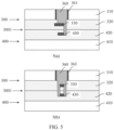
- FIG. 3 is a schematic diagram of a structure of a semiconductor device according to an embodiment of this application.
- the semiconductor device may include a first wafer 300, a second wafer 400, and a contact plug 360 for implementing vertical interconnection between the first wafer 300 and the second wafer 400.
- the first wafer 300 may include a first substrate 310, a first dielectric layer 320 on the first substrate 310, and a first connection pad 330 in the first dielectric layer 320.
- the second wafer 400 may include a second substrate 410, a second dielectric layer 420 on the second substrate 410, and a second connection pad 430 in the second dielectric layer 420.
- the first substrate 310 and the second substrate 410 may be semiconductor substrates, for example, Si substrates, Ge substrates, SiGe substrates, SOI (silicon on insulator, Silicon On Insulator), or GOI (germanium on insulator, Germanium On Insulator.
- the first substrate 310 and the second substrate 410 may also be substrates including a semiconductor with another element or a semiconductor with another compound, for example, GaAs, InP, or SiC; or may be laminated structures, for example, Si/SiGe; or may be other epitaxial structures, for example, SGOI (germanium silicon on insulator).
- the first substrate 310 and the second substrate 410 may be the same material, or may be different materials.
- the first substrate 310 and the second substrate 410 may be silicon substrates.
- All processes before bonding may be completed on the first substrate 310 and the second substrate 410.
- a device structure and an interconnection structure of electrically connected device structures are formed on the first substrate 310 and the second substrate 410.
- the device structure is covered by an inter-layer dielectric layer.
- the inter-layer dielectric layer may be silicon oxide.
- the interconnection structure is formed in a dielectric material.
- the device structure may be a MOS device, a storage device, and/or another passive device.
- the interconnection structure may be a multi-layer structure.
- the interconnection structure may include a contact plug, a via, or a connection layer.
- the connection layer may be located at a top layer of the interconnection structure.
- connection layer may include a plurality of connection pads.
- the interconnection structure may be a metal material, for example, tungsten, aluminum, or copper.
- connection layer at the top layer is shown. It may be understood that this is merely an example. In different designs and applications, an interconnection structure including a required quantity of layers may be formed according to a requirement.
- the same device structure or different device structures may be formed on the first substrate 310 and the second substrate 410.
- devices on the first substrate 310 and the second substrate 410 may be both DRAM devices, or both logic devices, or separately two devices in a DRAM device and a logic device, or separately two devices in a SRAM device and a logic device, or separately two devices in a CIS and an ISP.
- the same interconnection structure or different interconnection structures may be formed on the first substrate 310 and the second substrate 410.
- Connection pads in the interconnection structures on the first substrate 310 and the second substrate 410 may have the same structure or different structures.
- the first connection pad 330 in the interconnection structure on the first substrate 310 and the second connection pad 430 in the interconnection structure on the second substrate 410 are used as examples to describe interconnection structures between different wafers.
- the first connection pad 330 is a connection pad in the interconnection structure of the first wafer 300 before the bonding, and may be a top metal layer (top metal) in the first wafer 300.
- a material of the first connection pad 330 may be metal copper.
- the first connection pad 330 may be covered by the first dielectric layer 320, to implement isolation between different first connection pads 330.
- the first dielectric layer 320 may be a silicon oxide layer, or may be a stacked structure, for example, may include a silicon nitride layer and a silicon oxide layer on the silicon nitride layer.
- the second connection pad 430 is a connection pad in the interconnection structure of second first wafer 400 before the bonding, and may be a top metal layer in the second wafer 400.
- a material of the second connection pad 430 may be metal copper.
- the second connection pad 430 may be covered by the second dielectric layer 420, to implement isolation between different second connection pads 430.
- the second dielectric layer 420 may be a silicon oxide layer, or may be a stacked structure, for example, may include a silicon nitride layer and a silicon oxide layer on the silicon nitride layer.
- the first wafer 300 may be bonded to the second wafer 400.
- the first wafer 300 and the second wafer 400 may be two wafers in a plurality of bonded wafers.
- the front surface of the first wafer 300 may be bonded to the front surface of the second wafer 400.
- the front surface of the first wafer 300 may alternatively be bonded to the back surface of the second wafer 400.
- the back surface of the first wafer 300 may alternatively be bonded to the front surface of the second wafer 400.
- the back surface of the first wafer 300 may alternatively be bonded to the back surface of the second wafer 400.
- a surface used for bonding the first wafer 300 and the second wafer 400 is a bonding surface.
- a material layer used for bonding may be formed on the bonding surface.
- the bonding material layer may be an adhesive layer with a dielectric material, for example, silicon oxide or silicon nitride, to implement bonding between the two wafers by using molecular forces at the adhesive layer.
- first and second wafer are relative to each other, and are related to a bonding manner of the first wafer 300 and the second wafer.
- first wafer 300 may be used as an upper wafer
- second wafer 400 may be used as a lower wafer.
- front surface of the first wafer 300 is used as a bonding surface
- first wafer 300 is reversed, and original "upper” is changed to "lower”.
- back surface of the first wafer 300 is used as a bonding surface, the first wafer 300 is not reversed, and original "upper” is still “upper”.
- the two wafers are bonded by using dielectric layers, and electric connection is not implemented between the first connection pad 330 in the first wafer 300 and the second connection pad 430 in the second wafer 400. Therefore, connection between the first wafer 300 and the second wafer 400 needs to be implemented by using a vertical through hole 359.
- the first wafer 300 may be used as an upper wafer in the bonding structure. Etching is performed on the upper surface of the first wafer 300, to form the vertical through hole 359.
- etching may be performed on the front surface of the first wafer 300; or when the front surface of the first wafer 300 is used as a bonding surface 1001, etching may be performed on the back surface of the first wafer 300.
- etching may be performed on the upper surface of the first wafer by using a TSV technology, to form two through silicon vias passing through the first connection pad and the second connection pad. Then, a metal material is filled in the through silicon vias to form contact plugs. Afterwards, redistribution is performed on the upper surface of the first wafer, to establish connection between the two contact plugs.
- a path between the first connection pad and the second connection pad is relatively long, a size of each contact plug is limited by an etching process and cannot be reduced without limitation, and a distance between the contact plugs is also limited. Therefore, a plane area occupied by two three-dimensional interconnected structures in this process is relatively large.
- the contact plug is in contact with the first connection pad or the second connection pad
- sizes of the first connection pad and the second connection pad are also limited by the etching process, and match sizes of the contact plugs. Therefore, the size of the first connection pad and the size of the second connection pad are relatively large.
- the distance between the first connection pad and the second connection pad corresponds to a horizontal distance between the contact plugs. The minimum distance between the first connection pad and the second connection pad is also limited. Therefore, a distribution design is also limited.
- etching may be started from the upper surface of the first wafer 300.
- the first connection pad 330 is used as a blocking layer to form the vertical through hole 359.
- the upper surface of the first connection pad 330 and the upper surface and/or the sidewall of the second connection pad 430 are exposed.
- the first connection pad 330 may protect the first dielectric layer and the second dielectric layer under the first connection pad 330 from being etched.
- the formed contact plug 360 is in contact with the upper surface of the first connection pad 330, and also in contact with the upper surface and/or the sidewall of the second connection pad 430.
- the formed contact plug 360 is in contact with both the first connection pad 330 and the second connection pad 430, to form connection between the first connection pad 330 and the second connection pad 430.
- the contact plug 360 may enclose the first connection pad 330 on at least one side. A requirement for a plane size of the first connection pad 330 is not high. Therefore, a plane area of a device may be further reduced.
- the vertical through hole 359 may be a through hole with uneven dimensions from up to bottom. Specifically, the vertical through hole 359 may pass through the first wafer to the upper surface of the first connection pad 330, to expose the upper surface of the first connection pad 330. The vertical through hole 359 may further pass through the first wafer and the second wafer to the second connection pad 430 along the sidewall of the first connection pad 330, to expose the upper surface and/or the sidewall of the second connection pad 430. In other words, the through hole above the first connection pad 330 may have a relatively large size, the through hole between the first connection pad 330 and the second connection pad 430 may have a relatively small size.
- the vertical through hole 359 may expose the entire upper surface of the first connection pad 330, or may expose a part of the upper surface of the first connection pad 330.
- the vertical through hole 359 may expose the sidewall on one or more sides of the first connection pad 330, or may not expose the sidewall of the first connection pad 330. In this case, the sidewall of the first connection pad 330 is covered by a part of the first dielectric layer, to provide protection for the first connection pad 330.
- the vertical through hole 359 may expose the entire upper surface of the second connection pad 430, or may expose a part of the upper surface of the second connection pad 430.
- the vertical through hole 359 may expose the sidewall on one or more sides of the second connection pad 430, or may not expose the sidewall of the second connection pad 430. In this case, the sidewall of the second connection pad 430 is covered by the second dielectric layer.
- FIG. 4 is a schematic diagram of shapes of a first connection pad and a second connection pad according to an embodiment of this application.
- the first connection pad 330 may be polygonal or circular, and the second connection pad 430 may be polygonal or circular.
- the first connection pad 330 and the second connection pad 430 may have the same shape or different shapes. Certainly, a horizontal distance between the first connection pad 330 and the second connection pad 430 is relatively short.
- the first connection pad 330 and the second connection pad 430 may have overlapping projections in a vertical direction, or have no overlapping projection in a vertical direction.
- a polygon may be, for example, a strip.
- a circle may be, for example, a perfect circle or an oval.
- the first connection pad 330 is a strip
- the second connection pad 430 is also a strip.
- the first connection pad 330 and the second connection pad 430 may have the same size or different sizes.
- FIG. 5 is a schematic diagram of a structure of a semiconductor device according to an embodiment of this application.
- the second connection pad 430 and the first connection pad 330 may be disposed opposite to each other in a vertical direction.
- the vertical through hole 359 may expose the sidewalls of the second connection pad 430 and the first connection pad 330, and the exposed sidewalls of the second connection pad 430 and the first connection pad 330 are flush with each other.
- the contact plug 360 in the vertical through hole 359 is separately connected to the sidewall of the second connection pad 430 and the sidewall of the first connection pad 330, to electrically connect the second connection pad 430 and the first connection pad 330.
- the second connection pad 430 may be aligned with the first connection pad 330 on one side.
- the sidewall on one side of the first connection pad 330 exceeds the sidewall of the second connection pad 430 in the horizontal direction.
- the contact plug 360 may be in contact with the upper surface and the sidewall on one side of the first connection pad 330 and the sidewall on one side of the second connection pad 430. As shown in FIG.
- the second connection pad 430 may be aligned with the first connection pad 330 on a plurality of sides.
- the contact plug 360 may be in contact with the upper surface and the sidewall on a plurality of sides of the first connection pad 330 and the sidewall on a plurality of sides of the second connection pad 430.
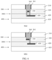
- FIG. 6 is a schematic diagram of a structure of another semiconductor device according to an embodiment of this application.
- the second connection pad 430 may be disposed opposite to the first connection pad 330 in the vertical direction.
- the sidewall on at least one side of the second connection pad 430 exceeds the sidewall of the first connection pad 330 in the horizontal direction.
- the formed vertical through hole 359 exposes at least a part of a surface on a side of the second connection pad 430 exceeding the first connection pad 330 in the horizontal direction, that is, exposes the upper surface adjacent to the sidewall of the second connection pad 430 exceeding the first connection pad 330 in the horizontal direction and exposes the sidewall and the upper surface adjacent to the sidewall of the second connection pad 430 exceeding the first connection pad 330 in the horizontal direction.
- the contact plug 360 filled in the vertical through hole 359 is at least in contact with the upper surface of the second connection pad 430.
- the vertical through hole 359 may further expose the upper surface of the first connection pad 330, so that the contact plug 360 can connect the first connection pad 330 and the second connection pad 430.
- the sidewall on one side of the second connection pad 430 may exceed the first connection pad 330 in the horizontal direction.
- the sidewall on one side of the second connection pad 430 may be aligned with the first connection pad 330, and the sidewall on another side of the second connection pad 430 exceeds the sidewall of the first connection pad 330 in the horizontal direction.
- the contact plug 360 may be in contact with the upper surface and the sidewall on a plurality of sides of the first connection pad 330, and the sidewall on one side and the upper surface on another side of the second connection pad 430. As shown in FIG.
- the sidewall on one side of the second connection pad 430 may exceed the first connection pad 330 in the horizontal direction, and the sidewall on another side wall of the second connection pad 430 is concave relative to the first connection pad 330.
- the contact plug 360 may be in contact with the upper surface and the sidewall on one side of the first connection pad 330, and the second connection pad 430 exceeds the upper surface on one side of the second connection pad 430 exceeding the first connection pad 330 in the horizontal direction, as shown in FIG. 6(b) .
- FIG. 7 is a schematic diagram of a structure of still another semiconductor device according to an embodiment of this application.
- the contact plug 360 may be in contact with the upper surface and the sidewall on one side of the first connection pad 330, and the second connection pad 430 exceeds the upper surface on one side of the first connection pad 330.
- the contact plug 360 may be in contact with the upper surface and the sidewall on a plurality of sides of the first connection pad 330 and the upper surface of the second connection pad 430.
- the contact plug 360 may be in contact with the upper surface and the sidewall on a plurality of sides of the first connection pad 330, and the upper surface and the sidewall on a plurality of sides of the second connection pad 430.
- a part of the first dielectric layer may be reserved between the contact plug 360 and the first connection pad 330, to provide protection for the first connection pad 330 in an etching process.
- the contact plug 360 may connect the first connection pad 330 and the second connection pad 430 from a plurality of sides of the first connection pad 330, to improve, to some extent, a contact area between the contact plug 360 and the second connection pad 430 and improve contact reliability between the contact plug 360 and the second connection pad 430.
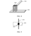
- FIG. 8 is a schematic diagram of a structure of a three-dimensional interconnection structure according to an embodiment of this application.
- FIG. 9 is a top view of a three-dimensional interconnection structure according to an embodiment of this application.
- the contact plug 360 forms an arch structure, to implement connection between the first connection pad 330 and the second connection pad 430.
- the contact plug 360 is formed on left and right sides of the first connection pad 330.
- a width between the left side and the right side of the first connection pad 330 may be relatively small.
- FIG. 10 is a schematic diagram of a structure of yet another semiconductor device according to an embodiment of this application.
- the second connection pad 430 and the first connection pad 330 are disposed in a staggered manner in the vertical direction. In other words, there is no overlapping region between the second connection pad 430 and the first connection pad 330 in a direction perpendicular to the bonding surface 1001. Therefore, a size of the top opening of the vertical through hole 359 is greater than or equal to the horizontal distance between the second connection pad 430 and the first connection pad 330.
- the vertical through hole 359 may expose the opposite sidewalls of the first connection pad 330 and the second connection pad 430, that is, expose the sidewall of the first connection pad 330 facing the second connection pad 430, and expose the sidewall of the second connection pad 430 facing the first connection pad 330.
- the vertical through hole 359 has even a horizontal size at different depths, so that the metal plug 360 in the vertical through hole 359 can connect the exposed sidewalls of the first connection pad 330 and the second connection pad 430, to implement electrical connection between the first connection pad 330 and the second connection pad 430.
- the size of the top opening of the vertical through hole 359 may be greater than the lateral sizes of the second connection pad 430 and the first connection pad 330.
- the vertical through hole 359 may further expose a part of the upper surface of the first connection pad 330 and/or a part of the upper surface of the second connection pad 430.
- a part of the first dielectric layer may be reserved for the sidewall of the first connection pad 330, to provide protection for the first connection pad 330, as shown in FIG. 10(b) .
- FIG. 11 is a schematic diagram of other shapes of a first connection pad and a second connection pad according to an embodiment of this application.
- a shape of the first connection pad 330 may be a slit shape or a comb tooth shape.
- a shape of the second connection pad 430 may be a polygon, a circle, a slit shape, or a comb tooth shape.
- the shape of the first connection pad 330 is a polygon or a circle
- the shape of the second connection pad 430 may be a slit shape or a comb tooth shape.
- the slit shape may be a single slit shape or a multi-slit shape.
- the slit shape may include a single slit shape with reference to FIG.
- a quantity of comb teeth in the comb tooth shape may be determined according to an actual case.
- the slit shape or the comb tooth shape may be considered as a combination of a plurality of lines.
- the formed vertical through hole 359 may expose or may not expose a sidewall of a connection pad with the slit shape or the comb tooth shape, provided that the vertical through hole 359 can expose both a part of the upper surface of the first connection pad 330 and a part of the upper surface of the second connection pad 430, to implement contact between the contact plug 360 and each of the first connection pad 330 and the second connection pad 430.
- FIG. 12 is a schematic diagram of a structure of still yet another semiconductor device according to an embodiment of this application.
- the second connection pad 430 is in the single slit shape.
- the contact plug 360 may be connected to the upper surface and the sidewall of the first connection pad 330 and the upper surface of the second connection pad 430.
- the contact plug 360 may be connected to the upper surface and the sidewall of the first connection pad 330 and the upper surface and the sidewall of the second connection pad 430.
- the second connection pad 430 is in a double slit shape.
- the contact plug 360 may be connected to the upper surface and the sidewall of the first connection pad 330 and the sidewall of the second connection pad 430.
- the vertical through hole 359 may be a through hole passing through the upper surface of the first wafer 300 to the upper surface of the first connection pad 330, and passing through the periphery of the first connection pad 330 to the upper surface of the second connection pad 430.
- the through hole exposes the upper surface of the first connection pad 330 and the upper surface and/or the sidewall of the second connection pad 430, to form the vertical through hole 359 with a relatively large size at an upper part and a relatively small size at a lower part.
- FIG. 13 is a schematic diagram of a structure of a further semiconductor device according to an embodiment of this application. Specifically, as shown in FIG. 3 , a size of the vertical through hole 359 in the first substrate 310 may be different from a size of the vertical through hole in the first dielectric layer 320. As shown in FIG. 13(a) and FIG. 13(c) , a size of the vertical through hole 359 above the upper surface of the first connection pad 330 may be different from a size of the vertical through hole 359 below the upper surface of the first connection pad 330. As shown in FIG.
- a size of the vertical through hole 359 above the lower surface of the first connection pad 330 may be different from a size of the vertical through hole 359 below the lower surface of the first connection pad 330.
- a size of the vertical through hole 359 above the upper surface of the second connection pad 430 may be different from a size of the vertical through hole 359 below the upper surface of the second connection pad 430.
- the semiconductor device provided in this embodiment of this application may further include a third wafer.
- FIG. 14 is a schematic diagram of a structure of still further semiconductor device according to an embodiment of this application.
- the first wafer 300, the second wafer 400, and the third wafer 500 form three stacked layers.
- the third wafer 500 may include a third substrate 510.
- a third dielectric layer 520 may be formed on the third substrate 510.
- the third dielectric layer 520 may have a third connection pad 530.
- the third wafer 500 may be disposed on the first wafer 300. Electrical connection is implemented between the third connection pad 530 in the third wafer 500 and the contact plug 360 through bonding between the first wafer 300 and the third wafer 500.
- the third connection pad 530 and the contact plug 360 may be connected (not shown in the figure) by using another contact plug formed by using a manufacturing process similar to the contact plug 360, after the dielectric layers of the first wafer 300 and the third wafer 500 are bonded.
- a bonding surface 5001 between the first wafer 300 and the third wafer 500 refer to FIG. 14 .
- the embodiments of this application provide the semiconductor device.
- the semiconductor device includes the first wafer, the second wafer, and the contact plug.
- the first wafer may include the first dielectric layer.
- the first dielectric layer has the first connection pad.
- the second wafer is bonded to the first wafer.
- the second wafer includes the second dielectric layer.
- the second dielectric layer has the second connection pad.
- the contact plug is a conductive material filled in the vertical through hole.
- the contact plug is configured to electrically connect the first connection pad and the second connection pad.
- the vertical through hole is a through hole that is formed through etching and that passes through the first wafer and partially passes through the second wafer to the upper surface and/or the sidewall of the second connection pad.
- the first connection pad is located in the vertical through hole.
- connection plug in the vertical through hole may be in contact with the upper layer of the first connection pad and the upper layer and/or the sidewall of the second connection pad, to implement electrical connection between the first connection pad and the second connection pad and implement vertical interconnection between the first wafer and the second wafer.
- the connection plug serves as a signal transmission path between the first connection pad and the second connection pad. This path is relatively short. Therefore, a signal delay is reduced.
- the vertical through hole is formed by using an etching process, and passes through the sidewall of the first connection pad to the second connection pad.
- the contact plug may be in contact with the second connection pad from the periphery of the first connection pad, to implement reliable connection between the contact plug and the second connection pad by using a simple process.
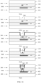
- FIG. 15 is a flowchart of a manufacturing method of a semiconductor device according to an embodiment of this application.
- FIG. 16 to FIG. 20 are schematic diagrams of a semiconductor device in a manufacturing process of the semiconductor device according to an embodiment of this application. The method may include the following steps:
- S101 Provide a first wafer 300 and a second wafer 400 between which bonding is completed, with reference to FIG. 16(a) , FIG. 17(a) , FIG. 18(a) , FIG. 19(a) , and FIG. 20(a) .
- the first wafer 300 may include a first substrate 310, a first dielectric layer 320 on the first substrate 310, and a first connection pad 330 in the first dielectric layer 320.
- the second wafer 400 may include a second substrate 410, a second dielectric layer 420 on the second substrate 410, and a second connection pad 430 in the second dielectric layer 420.
- the same device structure or different device structures may be formed on the first substrate 310 and the second substrate 410.
- devices on the first substrate 310 and the second substrate 410 may be both DRAM devices, or both logic devices, or respectively two devices of a DRAM device and a logic device, or separately two devices in a SRAM device and a logic device, or separately two devices in a CIS and an ISP.
- the first connection pad 330 is a connection pad in the interconnection structure of the first wafer 300 before the bonding, and may be a top metal layer (top metal) in the first wafer 300.
- a material of the first connection pad 330 may be metal copper.
- the first connection pad 330 may be covered by the first dielectric layer 320, to implement isolation between different first connection pads 330.
- the first dielectric layer 320 may be a silicon oxide layer, or may be a stacked structure, for example, may include a silicon nitride layer and a silicon oxide layer on the silicon nitride layer.
- the second connection pad 430 is a connection pad in the interconnection structure of second first wafer 400 before the bonding, and may be a top metal layer in the second wafer 400.
- a material of the second connection pad 430 may be metal copper.
- the second connection pad 430 may be covered by the second dielectric layer 420, to implement isolation between different second connection pads 430.
- the second dielectric layer 420 may be a silicon oxide layer, or may be a stacked structure, for example, may include a silicon nitride layer and a silicon oxide layer on the silicon nitride layer.
- a surface on which a device structure is formed on the first substrate 310 is used as a front surface of the first wafer 300, and a surface opposite to the surface on which a device is formed on the first substrate 310 is used as a back surface of the first wafer 300; and a surface on which a device structure is formed on the second substrate 410 is used as a front surface of the second wafer 400, and a surface opposite to the surface on which a device is formed on the second substrate 410 is used as a back surface of the second wafer 400.
- the first wafer 300 may be bonded to the second wafer 400.
- the first wafer 300 and the second wafer 400 may be two wafers in a plurality of bonded wafers.
- the front surface of the first wafer 300 may be bonded to the front surface of the second wafer 400.
- the front surface of the first wafer 300 may alternatively be bonded to the back surface of the second wafer 400.
- the back surface of the first wafer 300 may alternatively be bonded to the front surface of the second wafer 400.
- the back surface of the first wafer 300 may alternatively be bonded to the back surface of the second wafer 400.
- a material layer used for bonding may be formed on a surface used for bonding the first wafer 300 and the second wafer 400 is a bonding surface.
- the bonding material layer may be an adhesive layer with a dielectric material, for example, silicon oxide or silicon nitride, to implement bonding between the two wafers by using molecular forces at the adhesive layer.
- the two wafers are bonded by using dielectric layers, and vertical interconnection is not implemented between the first connection pad 330 in the first wafer 300 and the second connection pad 430 in the second wafer 400. Therefore, connection between the first wafer 300 and the second wafer 400 needs to be implemented.
- S102 Use the first connection pad as a blocking layer, etch the first wafer 300 from top to bottom to form a vertical through hole 359.
- the vertical through hole 359 passes through the first wafer to an upper surface of the first connection pad 330, passes through the first wafer and the second wafer to the second connection pad 430 along the sidewall of the first connection pad 330, and exposes an upper surface and/or a sidewall of the second connection pad 430.
- the first wafer 300 may be used as an upper wafer in the bonding structure. Etching is performed on the upper surface of the first wafer 300, to form the vertical through hole 359. It may be understood that, when the back surface of the first wafer 300 is used as a bonding surface 1001, etching may be performed on the front surface of the first wafer 300; or when the front surface of the first wafer 300 is used as a bonding surface 1001, etching may be performed on the back surface of the first wafer 300.
- the vertical through hole 359 may expose the entire upper surface of the first connection pad 330, or may expose a part of the upper surface of the first connection pad 330.
- the vertical through hole 359 may expose the sidewall on one or more sides of the first connection pad 330, or may not expose the sidewall of the first connection pad 330. In this case, the sidewall of the first connection pad 330 is covered by a part of the first dielectric layer, to provide protection for the first connection pad 330.
- the vertical through hole 359 may expose the entire upper surface of the second connection pad 430, or may expose a part of the upper surface of the second connection pad 430.
- the vertical through hole 359 may expose the sidewall on one or more sides of the second connection pad 430, or may not expose the sidewall of the second connection pad 430. In this case, the sidewall of the second connection pad 430 is covered by the second dielectric layer.
- the following uses bonding between the front surface of the first wafer 300 and the second wafer 400 as an example for description.
- the second connection pad 430 is disposed opposite to the first connection pad 330 in a vertical direction.
- the second connection pad 430 is located below the first connection pad 330.
- the sidewall of the second connection pad 430 may be flush with the sidewall of the first connection pad 330, or the sidewall of the second connection pad 430 exceeds the sidewall of the first connection pad 330 in the horizontal direction.
- a manner of forming the vertical through hole 359 may be specifically as follows: first etching the upper surface of the first wafer to obtain a first opening, where the first opening is located above the first connection pad 330, and a sidewall on at least one side of the first opening may exceed the sidewall of the first connection pad 330 in the horizontal direction.
- the first opening is deepened, to expose the first connection pad 330.
- Etching is performed in a position in which a bottom of the first opening exceeds the sidewall of the first connection pad 330 in the horizontal direction.
- a second opening to the second connection pad 430 may be formed around the periphery of the first connection pad 330, to form the vertical through hole 359.
- the first connection pad 330 may protect the first dielectric layer and the second dielectric layer under the first connection pad 330.
- a position of the second opening may be determined based on a position of the second connection pad 430 relative to the first connection pad 330.
- a direction in which the sidewall of the second connection pad 430 exceeds the sidewall of the first connection pad 330 in the horizontal direction may be consistent with a direction in which the sidewall of the second opening exceeds the sidewall of the first connection pad 330.
- the sidewall on a plurality of sides of the second connection pad 430 exceeds the sidewall of the first connection pad 330 in the horizontal direction.
- etching may be performed on the back surface of the first wafer 300, that is, etching is performed on the back surface of the first substrate 310 to form the first opening 350.
- the first opening 350 may be above the first connection pad 330, and the sidewall on a plurality of sides of the first opening 350 extends the sidewall of the first connection pad 330 in the horizontal direction.
- Etching of the first opening 350 may be stopped in a position of the lower surface of the first substrate 310, or etching may be performed on a part of the first dielectric layer 320 (not shown in the figure) and stopped in the first dielectric layer 320.
- An insulating layer 361 is deposited to protect the sidewall of the first opening 350. As shown in FIG.
- etching is performed on the bottom in the position in which the sidewall of the first opening 350 exceeds the first connection pad 330 in the horizontal direction (in this time of etching, the sidewall of the first connection pad 330 may be exposed, or a part of the first dielectric layer 320 may be reserved and the sidewall of the first connection pad 330 may be not exposed), to form a second opening 351 to the bonding surface 1001.
- the first connection pad 330 is used as a blocking layer, and the first opening 350 and the second opening 351 are deepened together, to remove the first dielectric layer 320 above the first connection pad 330 and the second dielectric layer 420 above the second connection pad 430, thereby forming the vertical through hole 359. As shown in FIG.
- the formed vertical through hole 359 exposes the upper surface of the first connection pad 330, and a part of the upper surface on a plurality of sides of the second connection pad 430 exceeding the first connection pad 330 in the horizontal direction.
- a part of the first dielectric layer 320 on the sidewall of the first connection pad 330 is reserved, to protect the first connection pad 330 and avoid damage or collapse caused due to etching performed on the first connection pad 330.
- the second dielectric layer of the sidewall of the second connection pad 430 may be etched to expose the sidewall of the second connection pad 430.
- etching is performed from the back surface of the first wafer 300.
- etching is performed from the back surface of the first substrate 310 to form the first opening 350.
- etching of the first opening 350 may be stopped in a position of a lower surface of the first substrate 310, or etching may be performed on a part of the first dielectric layer 320 (not shown in the figure) and stopped in the first dielectric layer 320.
- an insulating layer 361 is deposited to protect the sidewall of the first opening 350.
- etching is performed at a bottom in a position in which the sidewall of the first opening 350 exceeds the first connection pad 330 in the horizontal direction to form a second opening 351 to the bonding surface 1001.
- the first connection pad 330 is used as a blocking layer, and the first opening 350 and the second opening 351 are deepened together, so that the deepened second opening 351 is stopped at the lower surface of the second connection pad 430.
- the first connection pad 330 may protect the first dielectric layer and the second dielectric layer below the first connection pad 330, to form a vertical through hole 359.
- the vertical through hole 359 exposes the upper surface of the first connection pad 330, and a part of the upper surface and the sidewall on a plurality of sides of the second connection pad 430 extending the first connection pad 330.
- the dielectric layers of the sidewalls of the first connection pad 330 and the second connection pad 430 may be removed through etching, to expose the sidewalls of the first connection pad 330 and the second connection pad 430.
- steps shown in FIG. 16 Details are not described herein again.
- the second connection pad 430 is disposed opposite to the first connection pad 330 in the vertical direction.
- the second connection pad 430 is located below the first connection pad 330.
- the sidewall of the second connection pad 430 may be flush with the sidewall of the first connection pad 330, or the sidewall of the second connection pad 430 may exceed the sidewall of the first connection pad 330 in the horizontal direction.
- a third opening may be formed in the first wafer before bonding between wafers.
- the third opening is formed in the first dielectric layer around the first connection pad 330. In this way, an etching load after the bonding may be reduced.
- a manner of forming the vertical through hole may be specifically as follows: After the bonding between wafers, etching is performed on the upper surface of the first wafer to form a first opening, where the first opening is located above the first connection pad 330, and the sidewall on at least one side of the first opening may exceed the sidewall of the first connection pad 330 in the horizontal direction. In this way, the first opening may deepened to expose the first connection pad 330. In addition, the first opening may be connected to the third opening, and the third opening may be deepened. The deepened third opening may expose the second connection pad 430, to form the vertical through hole 359.
- the first connection pad 330 may protect the first dielectric layer and the second dielectric layer under the first connection pad 330.
- a position of the third opening may be determined based on a position of the second connection pad 430 relative to the first connection pad 330.
- a direction in which the sidewall of the second connection pad 430 exceeds the sidewall of the first connection pad 330 in the horizontal direction may be consistent with a direction in which the third opening is disposed in the first dielectric layer.
- a third opening 352 may be formed in the first wafer 300.
- the third opening 352 is formed in the first dielectric layer 320 around the first connection pad 330.
- etching may be performed on the first dielectric layer 320, to form the third opening 352 around the first connection pad 330.
- etching may be performed on the back surface of the first wafer 300, that is, etching is performed on the back surface of the first substrate 310 to form the first opening 350.
- the first opening 350 may be above the first connection pad 330, and the sidewall on a plurality of sides of the first opening 350 extends the sidewall of the first connection pad 330 in the horizontal direction.
- etching of the first opening 350 may be stopped in a position of the lower surface of the first substrate 310, or etching may be performed on a part of the first dielectric layer 320 (not shown in the figure) and stopped in the first dielectric layer 320. As shown in FIG.
- an insulating layer 361 is deposited to protect the sidewall of the first opening 350.
- the first connection pad 330 serves as a blocking layer.
- the first opening 350 is deepened to connect the first opening 350 to the third opening. Then, etching is further performed to deepen the third opening 352. Therefore, the deepened first opening 350 exposes the upper surface of the first connection pad, and the deepened third opening 352 exposes the upper surface of the second connection pad 430 to form the vertical through hole 359, as shown in FIG. 18(d) .
- the second dielectric layer of the sidewall of the second connection pad 430 may be etched to expose the sidewall of the second connection pad 430. Examples are not provided for description herein. In a direction in which the second connection pad 430 is flush with the first connection pad 330, the dielectric layers of the sidewalls of the first connection pad 330 and the second connection pad 430 may be removed through etching, to expose the sidewalls of the first connection pad 330 and the second connection pad 430. For specific operation steps, refer to steps shown in FIG. 18 . Details are not described herein again.
- the second connection pad 430 is disposed opposite to the first connection pad 330 in a vertical direction.
- the second connection pad 430 is located below the first connection pad 330.
- the sidewall of the second connection pad 430 may be flush with the sidewall of the first connection pad 330, or the sidewall of the second connection pad 430 exceeds the sidewall of the first connection pad 330 in the horizontal direction.
- a manner of forming the vertical through hole 359 may be specifically as follows: first etching the upper surface of the first wafer to obtain a first opening, where the first opening is located above the first connection pad 330, and a sidewall on at least one side of the first opening may exceed the sidewall of the first connection pad 330 in the horizontal direction.
- the first opening may be deepened, to expose the first connection pad 330.
- the first opening is further deepened.
- the first connection pad 330 may protect the first dielectric layer and the second dielectric layer below the first connection pad 330.
- Etching is performed on the first dielectric layer and the second dielectric layer in a position in which the first opening exceeds the first connection pad 330 in the horizontal direction.
- the deepened first opening around the first connection pad 330 may pass through the second connection pad 430 around the first connection pad 330, to form the vertical through hole 359.
- the sidewall on a plurality of sides of the second connection pad 430 exceeds the sidewall of the first connection pad 330 in the horizontal direction.
- Etching is performed on the back surface of the first wafer 300, that is, etching is performed on the back surface of the first substrate 310, to form the first opening 350.
- the first opening 350 may be above the first connection pad 330, and the sidewall on a plurality of sides of the first opening 350 exceeds the sidewall of the first connection pad 330.
- etching of the first opening 350 may be stopped in a position of the lower surface of the first substrate 310, or etching may be performed on a part of the first dielectric layer 320 (not shown in the figure) and stopped in the first dielectric layer 320.
- the insulating layer 361 is deposited to protect the sidewall of the first opening 350.
- the first opening 350 is deepened.
- the second connection pad 430 is used as an etching stop layer.
- the first connection pad 330 provides protection for the first dielectric layer and the second dielectric layer under the first connection pad 330 until the upper surface of the second connection pad 430 is exposed.
- the upper surface of the first connection pad 330 is also exposed in the deepened first opening 350 to form the vertical through hole 359.
- the second connection pad 430 is disposed opposite to the first connection pad 330 in a vertical direction.
- the second connection pad 430 is located below the first connection pad 330.
- the sidewall of the second connection pad 430 may be flush with the sidewall of the first connection pad 330, or the sidewall of the second connection pad 430 exceeds the sidewall of the first connection pad 330 in the horizontal direction.
- a manner of forming the vertical through hole 359 may be specifically as follows: etching the upper surface of the first wafer to form a fourth opening. A sidewall on at least one side of the fourth opening exceeds the sidewall of the first connection pad 330. Then, the first connection pad 330 may be used as a blocking layer.
- Etching is performed on an upper part of the first connection pad 330 and a bottom part of the fourth opening, to expose the upper surface of the first connection pad 330.
- the deepened fourth opening exposes the upper surface and/or the sidewall of the second connection pad 430.
- the first connection pad 330 may protect the first dielectric layer and the second dielectric layer below the first connection pad 330.
- the sidewall on a plurality of sides of the second connection pad 430 exceeds the sidewall of the first connection pad 330.
- Etching is performed on the back surface of the first wafer 300, that is, etching is performed on the back surface of the first substrate 310.
- An etching position is around the first connection pad 330.
- etching is stopped in a position of the lower surface or the upper surface of the first connection pad 330, to obtain the fourth opening 353.
- the insulating layer 361 is deposited to protect the sidewall of the fourth opening 353.
- Etching is performed on the first dielectric layer 320 on the upper part of the first connection pad 330 and the first dielectric layer 320 and the second dielectric layer 420 at the bottom of the fourth opening 353 around the first connection pad 330, to expose the upper surface and the sidewall of the first connection pad 330 and the upper surface of the second connection pad 430, thereby forming the vertical through hole 359, as shown in FIG. 20(d) .
- the first connection pad 330 of the upper-layer wafer is used as a blocking layer; and etching is stopped when the second connection layer 430 of the lower-layer wafer is exposed.
- the first connection pad 330 is a conductive material.
- a material with relatively large etch selectivity may be set for the first dielectric layer and the second dielectric layer, for example, a metal material or a doped semiconductor material. Etching selectivity between metal and a dielectric layer is relatively large, for example, SiO 2 :Al is close to 20:1, and SiO 2 :W is close to 80:1.
- the first connection pad 330 and the second connection layer 430 are not greatly damaged, to ensure that the first connection pad 330 still exists before etching is performed on the second connection layer 430 until etching is performed on both the first dielectric layer 320 and the second dielectric layer 420. Etching is stopped at the second connection layer 430 of the lower wafer.
- the etching process is relatively simple.
- S103 Fill the vertical through hole 359 with a conductive material to form a contact plug 360, with reference to FIG. 16(e) , FIG. 17(e) , FIG. 18(e) , FIG. 19(e) , and FIG. 20(e) .
- etching may be started from the upper surface of the first wafer 300, to form the vertical through hole 359 as the vertical through hole 359.
- the upper surface of the first connection pad 330 and the upper surface and/or the sidewall of the second connection pad 430 are exposed.
- the formed contact plug 360 is in contact with the upper surface of the first connection pad 330, and also in contact with the upper surface and/or the sidewall of the second connection pad 430.
- the formed contact plug 360 is in contact with both the first connection pad 330 and the second connection pad 430, to implement electrical connection between the first connection pad 330 and the second connection pad 430.
- the contact plug 360 is formed in the vertical through hole 359.
- a conductive material may be formed in the vertical through hole 359 in an electroplating manner or a deposition manner. Then, the conductive material outside the vertical through hole 359 is removed by using a planarization process, for example, a chemical mechanical polishing process, to form the contact plug 360.
- a material of the contact plug 360 may be copper or aluminum, or may be another conductive metal material or a non-metal material, for example, may be doped silicon.
- the first wafer and the second wafer that are bonded are provided.
- the first wafer includes the first dielectric layer.
- the first dielectric layer has the first connection pad.
- the second wafer includes the second dielectric layer.
- the second dielectric layer has the second connection pad.
- the first connection pad is used as a blocking layer.
- Etching is performed on the first wafer from top to bottom to form the vertical through hole.
- Thee vertical through hole passes through the first wafer to the upper surface of the first connection pad, passes through the second wafer to the second connection pad along the sidewall of the first connection pad, and exposes the upper surface and/or the sidewall of the second connection pad.
- the conductive material is filled in the vertical through hole to form the contact plug.
- the vertical through hole may expose the upper surface of the first wafer and the upper surface and/or the sidewall of the second connection pad.
- the contact plug in the vertical through hole may be in contact with both the first connection pad and the second connection pad, to implement electrical connection between the first connection pad and the second connection pad.
- the contact plug serves as a signal transmission path between the first connection pad and the second connection pad. This path is relatively short. Therefore, a signal delay is reduced.
- the vertical through hole is formed by using an etching process, and passes through the sidewall of the first connection pad to the second connection pad.
- the contact plug may be in contact with the second connection pad from the periphery of the first connection pad, to implement reliable connection between the contact plug and the second connection pad by using a simple process.
- only one metal plug exists, and therefore, a distance between two metal plugs does not need to be considered. Therefore, a lateral size may be reduced to some extent, to reduce a device size and improve device integration.
Landscapes
- Internal Circuitry In Semiconductor Integrated Circuit Devices (AREA)
Applications Claiming Priority (1)
| Application Number | Priority Date | Filing Date | Title |
|---|---|---|---|
| PCT/CN2020/085375 WO2021208078A1 (fr) | 2020-04-17 | 2020-04-17 | Structure semi-conductrice et son procédé de fabrication |
Publications (2)
| Publication Number | Publication Date |
|---|---|
| EP4131374A1 true EP4131374A1 (fr) | 2023-02-08 |
| EP4131374A4 EP4131374A4 (fr) | 2023-05-31 |
Family
ID=78083516
Family Applications (1)
| Application Number | Title | Priority Date | Filing Date |
|---|---|---|---|
| EP20931045.7A Pending EP4131374A4 (fr) | 2020-04-17 | 2020-04-17 | Structure semi-conductrice et son procédé de fabrication |
Country Status (6)
| Country | Link |
|---|---|
| US (1) | US20230031151A1 (fr) |
| EP (1) | EP4131374A4 (fr) |
| JP (1) | JP2023521483A (fr) |
| KR (1) | KR20230002752A (fr) |
| CN (1) | CN114981962B (fr) |
| WO (1) | WO2021208078A1 (fr) |
Family Cites Families (20)
| Publication number | Priority date | Publication date | Assignee | Title |
|---|---|---|---|---|
| US5899738A (en) * | 1997-05-23 | 1999-05-04 | Taiwan Semiconductor Manufacturing Company, Ltd. | Method for making metal plugs in stacked vias for multilevel interconnections and contact openings while retaining the alignment marks without requiring extra masking steps |
| JP2011049250A (ja) * | 2009-08-25 | 2011-03-10 | Renesas Electronics Corp | 半導体装置およびその製造方法 |
| JP5957840B2 (ja) * | 2011-10-04 | 2016-07-27 | ソニー株式会社 | 半導体装置の製造方法 |
| US20130264688A1 (en) * | 2012-04-06 | 2013-10-10 | Omnivision Technologies, Inc. | Method and apparatus providing integrated circuit system with interconnected stacked device wafers |
| EP2859585A4 (fr) * | 2012-06-07 | 2016-01-27 | Rensselaer Polytech Inst | Utilisation d'un amortissement élastique de revêtement conforme pour réduire la contrainte d'interconnexions en silicium traversantes (ist) dans l'intégration tridimensionnelle |
| US9536777B2 (en) * | 2013-03-13 | 2017-01-03 | Taiwan Semiconductor Manufacutring Company, Ltd. | Interconnect apparatus and method |
| CN104051423B (zh) * | 2013-03-13 | 2018-02-16 | 台湾积体电路制造股份有限公司 | 互连装置和方法 |
| CN104377164A (zh) * | 2014-09-28 | 2015-02-25 | 武汉新芯集成电路制造有限公司 | 一种晶圆跨硅穿孔互连工艺 |
| KR102387948B1 (ko) * | 2015-08-06 | 2022-04-18 | 삼성전자주식회사 | Tsv 구조물을 구비한 집적회로 소자 |
| EP3531445B1 (fr) * | 2016-09-07 | 2020-06-24 | IMEC vzw | Procédé permettant de lier et d'interconnecter des dispositifs à circuits intégrés |
| US9748175B1 (en) * | 2016-11-18 | 2017-08-29 | Taiwan Semiconductor Manufacturing Co., Ltd. | Conductive structure in semiconductor structure and method for forming the same |
| US10522468B2 (en) * | 2017-07-31 | 2019-12-31 | Taiwan Semiconductor Manufacturing Company, Ltd. | Interconnect structure and method |
| KR102538174B1 (ko) * | 2017-12-26 | 2023-05-31 | 삼성전자주식회사 | 비아 플러그를 갖는 반도체 소자 |
| US11222836B2 (en) * | 2017-12-30 | 2022-01-11 | Intel Corporation | Zero-misalignment two-via structures |
| JP7746012B2 (ja) * | 2018-01-23 | 2025-09-30 | ルミエンス フォトニクス アイエヌシー. | 高性能の三次元半導体構造の製造方法、及びこの製造方法から生成される構造 |
| CN109148360B (zh) * | 2018-08-28 | 2019-12-03 | 武汉新芯集成电路制造有限公司 | 半导体器件制作方法 |
| CN111564420B (zh) * | 2018-09-21 | 2022-09-27 | 联华电子股份有限公司 | 具有散热结构的高电阻晶片及其制作方法 |
| CN109192747A (zh) * | 2018-10-31 | 2019-01-11 | 德淮半导体有限公司 | 图像传感器的形成方法 |
| CN109449091B (zh) * | 2018-11-05 | 2020-04-10 | 武汉新芯集成电路制造有限公司 | 半导体器件的制作方法 |
| CN110767605B (zh) * | 2019-11-04 | 2022-10-18 | 武汉新芯集成电路制造有限公司 | 一种金属衬垫的形成方法 |
-
2020
- 2020-04-17 KR KR1020227039876A patent/KR20230002752A/ko active Pending
- 2020-04-17 EP EP20931045.7A patent/EP4131374A4/fr active Pending
- 2020-04-17 CN CN202080093552.5A patent/CN114981962B/zh active Active
- 2020-04-17 JP JP2022562869A patent/JP2023521483A/ja active Pending
- 2020-04-17 WO PCT/CN2020/085375 patent/WO2021208078A1/fr not_active Ceased
-
2022
- 2022-10-14 US US17/966,034 patent/US20230031151A1/en active Pending
Also Published As
| Publication number | Publication date |
|---|---|
| KR20230002752A (ko) | 2023-01-05 |
| JP2023521483A (ja) | 2023-05-24 |
| CN114981962A (zh) | 2022-08-30 |
| CN114981962B (zh) | 2025-05-30 |
| EP4131374A4 (fr) | 2023-05-31 |
| WO2021208078A1 (fr) | 2021-10-21 |
| US20230031151A1 (en) | 2023-02-02 |
Similar Documents
| Publication | Publication Date | Title |
|---|---|---|
| JP5460713B2 (ja) | ウェハ貫通ビアおよびこれを作成する方法 | |
| US8587121B2 (en) | Backside dummy plugs for 3D integration | |
| US8421238B2 (en) | Stacked semiconductor device with through via | |
| US11973006B2 (en) | Self-aligned contact openings for backside through substrate vias | |
| US7678696B2 (en) | Method of making through wafer vias | |
| KR102833169B1 (ko) | 반도체 장치 및 반도체 장치의 제조 방법 | |
| CN107768305B (zh) | 半导体器件及其制造方法 | |
| CN112447641B (zh) | 半导体器件 | |
| KR20150058778A (ko) | 반도체 장치 및 그 제조 방법, 상기 반도체 장치를 포함하는 반도체 패키지 및 그 제조 방법 | |
| CN111725218B (zh) | 垂直半导体器件 | |
| US12463165B2 (en) | Bonding structure and manufacturing method therefor | |
| KR20190063110A (ko) | 반도체 소자 및 이를 포함하는 반도체 웨이퍼, 그리고 반도체 패키지 | |
| CN103515302A (zh) | 半导体元件与制作方法 | |
| TWI670857B (zh) | 記憶體結構及其形成方法 | |
| CN110783265A (zh) | 一种半导体器件及其制作方法 | |
| US20230031151A1 (en) | Semiconductor structure and manufacturing method thereof | |
| US12400938B2 (en) | Semiconductor device including a through silicon via structure and method of fabricating the same | |
| KR102916127B1 (ko) | 반도체 장치 제조 방법 | |
| US20250364349A1 (en) | Dummy features for dissipating heat in packages including advanced semiconductor chips | |
| EP2648214B1 (fr) | Procédés de production d'un dispositif semi-conducteur avec interconnexion traversant le substrat | |
| KR20250050582A (ko) | 반도체 소자 | |
| KR20230169663A (ko) | 본딩형 반도체 소자 | |
| TWI527152B (zh) | 半導體裝置及其製作方法 | |
| KR20140131786A (ko) | 반도체 소자 및 그 제조 방법 |
Legal Events
| Date | Code | Title | Description |
|---|---|---|---|
| STAA | Information on the status of an ep patent application or granted ep patent |
Free format text: STATUS: THE INTERNATIONAL PUBLICATION HAS BEEN MADE |
|
| PUAI | Public reference made under article 153(3) epc to a published international application that has entered the european phase |
Free format text: ORIGINAL CODE: 0009012 |
|
| STAA | Information on the status of an ep patent application or granted ep patent |
Free format text: STATUS: REQUEST FOR EXAMINATION WAS MADE |
|
| 17P | Request for examination filed |
Effective date: 20221026 |
|
| AK | Designated contracting states |
Kind code of ref document: A1 Designated state(s): AL AT BE BG CH CY CZ DE DK EE ES FI FR GB GR HR HU IE IS IT LI LT LU LV MC MK MT NL NO PL PT RO RS SE SI SK SM TR |
|
| A4 | Supplementary search report drawn up and despatched |
Effective date: 20230503 |
|
| RIC1 | Information provided on ipc code assigned before grant |
Ipc: H01L 27/146 20060101ALI20230425BHEP Ipc: H01L 23/00 20060101ALI20230425BHEP Ipc: H01L 25/065 20230101ALI20230425BHEP Ipc: H01L 23/48 20060101ALI20230425BHEP Ipc: H01L 21/768 20060101ALI20230425BHEP Ipc: H01L 23/538 20060101AFI20230425BHEP |
|
| DAV | Request for validation of the european patent (deleted) | ||
| DAX | Request for extension of the european patent (deleted) | ||
| GRAP | Despatch of communication of intention to grant a patent |
Free format text: ORIGINAL CODE: EPIDOSNIGR1 |
|
| STAA | Information on the status of an ep patent application or granted ep patent |
Free format text: STATUS: GRANT OF PATENT IS INTENDED |
|
| RIC1 | Information provided on ipc code assigned before grant |
Ipc: H01L 23/538 20060101AFI20251201BHEP Ipc: H01L 21/768 20060101ALI20251201BHEP Ipc: H01L 23/48 20060101ALI20251201BHEP Ipc: H01L 25/065 20230101ALI20251201BHEP Ipc: H01L 23/00 20060101ALI20251201BHEP Ipc: H10F 39/00 20250101ALI20251201BHEP |
|
| INTG | Intention to grant announced |
Effective date: 20260102 |
|
| P01 | Opt-out of the competence of the unified patent court (upc) registered |
Free format text: CASE NUMBER: UPC_APP_0008549_4131374/2026 Effective date: 20260303 |
|
| GRAS | Grant fee paid |
Free format text: ORIGINAL CODE: EPIDOSNIGR3 |
|
| GRAA | (expected) grant |
Free format text: ORIGINAL CODE: 0009210 |
|
| STAA | Information on the status of an ep patent application or granted ep patent |
Free format text: STATUS: THE PATENT HAS BEEN GRANTED |