EP4131375A1 - Anzeigetafel und anzeigevorrichtung - Google Patents
Anzeigetafel und anzeigevorrichtung Download PDFInfo
- Publication number
- EP4131375A1 EP4131375A1 EP20897674.6A EP20897674A EP4131375A1 EP 4131375 A1 EP4131375 A1 EP 4131375A1 EP 20897674 A EP20897674 A EP 20897674A EP 4131375 A1 EP4131375 A1 EP 4131375A1
- Authority
- EP
- European Patent Office
- Prior art keywords
- pad
- layer
- electrode
- display
- display panel
- Prior art date
- Legal status (The legal status is an assumption and is not a legal conclusion. Google has not performed a legal analysis and makes no representation as to the accuracy of the status listed.)
- Granted
Links
Images


Classifications
-
- H—ELECTRICITY
- H10—SEMICONDUCTOR DEVICES; ELECTRIC SOLID-STATE DEVICES NOT OTHERWISE PROVIDED FOR
- H10K—ORGANIC ELECTRIC SOLID-STATE DEVICES
- H10K59/00—Integrated devices, or assemblies of multiple devices, comprising at least one organic light-emitting element covered by group H10K50/00
- H10K59/10—OLED displays
- H10K59/12—Active-matrix OLED [AMOLED] displays
- H10K59/131—Interconnections, e.g. wiring lines or terminals
-
- G—PHYSICS
- G09—EDUCATION; CRYPTOGRAPHY; DISPLAY; ADVERTISING; SEALS
- G09G—ARRANGEMENTS OR CIRCUITS FOR CONTROL OF INDICATING DEVICES USING STATIC MEANS TO PRESENT VARIABLE INFORMATION
- G09G3/00—Control arrangements or circuits, of interest only in connection with visual indicators other than cathode-ray tubes
- G09G3/006—Electronic inspection or testing of displays and display drivers, e.g. of LED or LCD displays
-
- H—ELECTRICITY
- H10—SEMICONDUCTOR DEVICES; ELECTRIC SOLID-STATE DEVICES NOT OTHERWISE PROVIDED FOR
- H10K—ORGANIC ELECTRIC SOLID-STATE DEVICES
- H10K50/00—Organic light-emitting devices
- H10K50/80—Constructional details
- H10K50/84—Passivation; Containers; Encapsulations
- H10K50/844—Encapsulations
-
- H—ELECTRICITY
- H10—SEMICONDUCTOR DEVICES; ELECTRIC SOLID-STATE DEVICES NOT OTHERWISE PROVIDED FOR
- H10K—ORGANIC ELECTRIC SOLID-STATE DEVICES
- H10K71/00—Manufacture or treatment specially adapted for the organic devices covered by this subclass
- H10K71/70—Testing, e.g. accelerated lifetime tests
-
- H—ELECTRICITY
- H10—SEMICONDUCTOR DEVICES; ELECTRIC SOLID-STATE DEVICES NOT OTHERWISE PROVIDED FOR
- H10P—GENERIC PROCESSES OR APPARATUS FOR THE MANUFACTURE OR TREATMENT OF DEVICES COVERED BY CLASS H10
- H10P74/00—Testing or measuring during manufacture or treatment of wafers, substrates or devices
-
- H—ELECTRICITY
- H10—SEMICONDUCTOR DEVICES; ELECTRIC SOLID-STATE DEVICES NOT OTHERWISE PROVIDED FOR
- H10W—GENERIC PACKAGES, INTERCONNECTIONS, CONNECTORS OR OTHER CONSTRUCTIONAL DETAILS OF DEVICES COVERED BY CLASS H10
- H10W46/00—Marks applied to devices, e.g. for alignment or identification
-
- H—ELECTRICITY
- H10—SEMICONDUCTOR DEVICES; ELECTRIC SOLID-STATE DEVICES NOT OTHERWISE PROVIDED FOR
- H10K—ORGANIC ELECTRIC SOLID-STATE DEVICES
- H10K59/00—Integrated devices, or assemblies of multiple devices, comprising at least one organic light-emitting element covered by group H10K50/00
- H10K59/10—OLED displays
- H10K59/12—Active-matrix OLED [AMOLED] displays
- H10K59/121—Active-matrix OLED [AMOLED] displays characterised by the geometry or disposition of pixel elements
- H10K59/1213—Active-matrix OLED [AMOLED] displays characterised by the geometry or disposition of pixel elements the pixel elements being TFTs
Definitions
- the present disclosure relates to the field of display technology, and in particular to a display panel and a display device.
- a display panel including: A silicon-based substrate, including a display region and a peripheral region surrounding the display region.
- a driving layer formed in the silicon-based substrate, and including a plurality of first transistors located in the display region.
- a first electrode layer disposed on a side of the driving layer away from the silicon-based substrate, and including a plurality of first electrodes located in the display region, and each of the first electrodes is electrically connected to each of the first transistors.
- a second electrode layer disposed on a side of the organic light emitting layer away from the driving layer, and including a second electrode located in the display region and an electrode ring located in the peripheral region, the electrode ring is configure to surround the second electrode and is connected to the second electrode;
- a plurality of pads located in the peripheral region at at least one side of the display region, the plurality of pads including a display signal access pad and a test signal access pad, and the test signal access pad is located at both sides of the display signal access pad.
- each of the first transistors includes an active region formed in the silicon-based substrate, two doped regions located in the active region, a channel region located between the two doped regions, and a gate electrode located on the channel region, the two doped regions respectively form a first pole and a second pole, and the second pad is electrically connected to the active region of each of the first transistors.
- the test signal access pad also includes a second group of test phase access pads, and the second group of test phase access pads include a third pad and a fourth pad, the third pad is electrically connected to the electrode ring, and the fourth pad is electrically connected to the silicon-based substrate.
- the peripheral region includes a bonding area, the third pad, the fourth pad and a plurality of display signal access pads are located in the bonding area.
- the first pad and the third pad are located on a same side of the display signal access pad, and the second pad and the fourth pad are located on the other side of the display signal access pad.
- the display panel is provided with one first pad and one second pad.
- the display panel is provided with one third pad and one fourth pad.
- a connection line which is electrically connected to the second pad and the fourth pad.
- a plurality of detection lines which are connected to the connection line, and each of the detection lines is electrically connected to the active region of a row of first transistors respectively.
- the first pad is electrically connected to the electrode ring through a conducting wire.
- the display panel further includes: a second transistor, which is formed in the peripheral region of the silicon-based substrate, and includes an active region formed in the silicon-based substrate, two doped regions in the active region, a channel region between the two doped regions and a gate electrode located on the channel region, the two doped regions form a first pole and a second pole respectively; the second pole of the second transistor is electrically connected to the electrode ring, and the first pad is electrically connected to the first pad and the gate electrode of the second transistor.
- a second transistor which is formed in the peripheral region of the silicon-based substrate, and includes an active region formed in the silicon-based substrate, two doped regions in the active region, a channel region between the two doped regions and a gate electrode located on the channel region, the two doped regions form a first pole and a second pole respectively; the second pole of the second transistor is electrically connected to the electrode ring, and the first pad is electrically connected to the first pad and the gate electrode of the second transistor.
- the driving layer includes:
- a gate insulating layer which is disposed on a channel region on a side of the silicon-based substrate.
- a gate layer which is disposed on a side of the gate insulating layer away from the silicon-based substrate.
- a first planarization layer which is disposed on a side of the silicon-based substrate and is configured to cover the gate insulating layer and the gate layer;
- a first conductive layer which is disposed on a side of the first planarization layer away from the silicon-based substrate.
- a dielectric layer which is provided on a side of the first planarization layer away from the silicon-based substrate and is configured to cover the first conductive layer.
- a second conductive layer which is disposed on a side of the dielectric layer away from the silicon-based substrate.
- the display panel further includes:
- a color film layer which is disposed on a side of the first packaging layer away from the second electrode layer.
- a second packaging layer which is disposed on a side of the color film layer away from the first packaging layer, the third pad and the fourth pad are exposed from the second packaging layer.
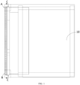
- the silicon-based substrate 20 includes a display region and a peripheral region surrounding the display region;
- the driving layer 30 is formed in the silicon-based substrate 20 and includes a plurality of first transistors located in the display region;
- the first electrode layer is disposed on the side of the driving layer 30 away from the silicon-based substrate 20, and includes a plurality of first electrodes 40 located in the display region, and each first electrode 40 is electrically connected to each first transistor;
- the organic light emitting layer 60 is disposed on the side of the first electrode layer away from the driving layer 30;
- the second electrode layer 70 is disposed on the side of the organic light emitting layer 60 away from the driving layer 30, and includes a second electrode 720 located in the display region and an electrode ring 710 located in the peripheral region, the electrode ring 710 surrounds the second electrode 720 and is connected to the second electrode 720;
- a plurality of pads are located in the peripheral region at at least one side of the display region, the plurality of pads include display signal access pads and test signal access pads, and the test
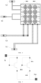
- each first electrode 40 is connected to a first transistor, and the silicon-based substrate corresponding to each first transistor is connected to the second pad 52; the test signal is input through the first pad 51 and the second pad 52 to form a voltage difference between the first electrode 40 and the second electrode 720, thereby illuminating the pixel unit, performing an IVL test and collecting test data to achieve the ILV test purpose.
- the silicon-based substrate 20 constitutes a silicon-based OLED display panel
- the embodiment of the present disclosure provides a top-emission type silicon-based OLED display panel
- C1 in the figure refers to the first transistor
- each first transistor includes an active region 380 formed in the silicon-based substrate, two doped regions located in the active region 380, a channel region located between the two doped regions, and a gate electrode 320 located on the channel region.
- the two doped regions respectively form a first pole 310 and a second pole 330, and the second pad 52 is electrically connected to the active region 380 of each first transistor.
- the first transistor is a P-type MOS transistor
- the active region 380 is an N-type doped region
- the first pole 310 and the second pole 320 are a P-type doped region on the silicon-based substrate
- the second pole 330 of the first transistor is the drain electrode
- the first electrode 310 is the source electrode.
- the silicon-based substrate corresponding to each first transistor is the active region 380 of the first transistor, and the active region 380 of the first transistor is connected to the VDD test signal through the second pad 52, the PN junction is turned on through the forward bias, so that the VDD test signal is transmitted to the anode.
- the electrode ring 710 is a cathode ring
- the cathode ring is a ring-shaped wiring that provides a cathode common voltage (negative) at the periphery of the display region, when the cathode is evaporated, it covers the display region and overlaps the cathode ring, thereby providing negative voltage for the common cathode in the entire display region.
- the drain electrode of the first transistor is connected to the first electrode 40 through the second conductive layer 350 and the first conductive layer 340, through the arrangement of the second conductive layer 350 and the first conductive layer 340, the wiring area is reduced and the resolution is improved.
- the first electrode 40 is electrically connected to the second conductive layer 350 through the contact holes 360
- the second conductive layer 350 is electrically connected to the first conductive layer 340 through the contact holes 360
- the first conductive layer 340 is electrically connected to the second electrode 330 through the contact holes 360
- the gate 320 is electrically connected to the first electrode 310 through the contact holes 360, respectively.
- the contact hole 360 is a tungsten hole.
- C2 in FIG. 4 refers to the second transistor electrically connected to the electrode ring 710
- a second transistor is formed in the peripheral region of the silicon-based substrate, including an active region formed in the silicon-based substrate, two doped regions in the active region, a channel region between the two doped regions and a gate electrode 393 located on the channel region, the two doped regions form a first pole 391 and a second pole 392 respectively.
- the second pole 392 of the second transistor is electrically connected to the electrode ring 710
- the first pad 51 is electrically connected to the first pad 391 and the gate electrode 393 of the second transistor.
- the first pad 51 is electrically connected to the first pole 391 and the gate electrode 393 of the second transistor, so that Vcom is transmitted to the second electrode 720 through the electrode ring 710 and then a voltage difference is formed between the first electrode 40 and the second electrode 720, thereby illuminating the pixel unit to conduct IVL test and collect test data to achieve the purpose of ILV testing.
- the first pole 391 can be a source electrode
- the second pole 392 can be a drain electrode.
- the first pad 51 may also be electrically connected to the electrode ring 710 through a conducting wire, so that the Vcom can be transmitted to the second electrode 720 through the electrode ring 710, so that a voltage difference is formed between the first electrode 40 and the second electrode 720, and then the pixel unit is lighted to perform an IVL test and collect test data to achieve the purpose of the ILV test.
- the first pad 51 and the electrode ring 710 are directly electrically connected through a conducting wire, which reduces the process difficulty.
- the peripheral region of the silicon-based substrate includes a bonding area, the third pad 53, the fourth pad 54 and a plurality of display signal access pads are located in the bonding area, and the display signal access pads are the bonding pads 41. Since the display panel is covered with multiple organic and inorganic materials during the packaging process, the first pad 51 and the second pad 52 will be covered, and the MIT test cannot be performed through the first pad 51 and the second pad 52 after packaging.
- the third pad 53, the fourth pad 54 and a plurality of display signal access pads can be simultaneously formed in the bonding area, the third pad 53 and the fourth pad 54 and together with other bonding pads 41 need to be provided with a photoresist layer, and then laser ablation is used to ablate the photoresist layer together with the organic and inorganic materials in the evaporation and packaging process to expose the metal on the surface of each pad to meet the pinning requirements of the MIT test probe boards.
- the third pad 53 is electrically connected to the electrode ring 710
- the fourth pad 54 is electrically connected to the silicon-based substrate, so that the MIT test is performed through the third pad 53 and the fourth pad 54.
- the third pad 53 and the fourth pad 54 are respectively arranged adjacent to the display signal access pads.
- a plurality of bonding pads 41 are disposed on the bonding area at one side of the silicon-based substrate 20, and each bonding pad 41 is located between the third pad 53 and the fourth pad 54.
- the third pad 53 and the fourth pad 54 are disposed in the bonding area and located at both ends of the bonding pad 41, which will not affect the layout of the bonding pads 41, the third pad 53, the fourth pad 54 and the bonding pad 41 can be exposed through the same laser ablation process, which reduces the process difficulty and process cost.
- the first pad 51, the second pad 52, the third pad 53, and the fourth pad 54 are located between the bonding pads 41 and the Flexible Printed Circuit (FPC) Mark, the Mark provides common positionable circuit patterns for all steps in the assembly process of Flexible Printed Circuit (FPC).
- the first pad 51 and the third pad 53 are located on the same side of the display signal access pads, and the second pad 52 and the fourth pad 54 are located on the other side of the display signal access pads.
- the display panel is only provided with one first pad 51 and one second pad 52, and the second pad 52 is electrically connected to the active region of each MOS transistor.
- the IVL test can be realized by only two pads, so that the number of pads is minimized, and the layout of the first pad 51 and the second pad 52 on the silicon-based substrate 20 is convenient.
- the display panel 10 is only provided with one third pad 53 and one fourth pad 54, and the fourth pad 54 is electrically connected to the active region of each MOS transistor.
- the MIT test can be realized by only two pads, so that the number of pads is minimized, and the layout of the third pad 53 and the fourth pad 54 on the silicon-based substrate 20 is convenient.
- the fourth pad 54 is connected to the second pad 52.
- the fourth pad 54 and the second pad 52 can be located on the same side of the silicon-based substrate 20, after the second pad 52 is connected to each first electrode 40 through a conducting wire, the fourth pad 54 can be connected to the second pad 52 through a conducting wire, so that the fourth pad 54 is indirectly connected to each first electrode 40, which can reduce the number of the conducting wires connecting to each first electrode 40, thereby reducing the difficulty of the fabricating process of the display panel 10.
- the first pad 51, the second pad 52, the third pad 53, and the fourth pad 54 are arranged in the same layer as the first electrode 40.
- the first pad 51, the second pad 52, the third pad 53, and the fourth pad 54 can be formed through the same process, the form of the first pad 51, the second pad 52, the third pad 53, and the fourth pad 54 is facilitated, and the fabricating process difficulty of the display panel 10 is reduced.
- the driving layer 30 further includes: a connection line 381 and a plurality of detection lines 382.
- the connection line 381 is electrically connected to the second pad 52 and the fourth pad 54; the plurality of detection lines 382 are connected to the connection line 38, and each detection line 382 is electrically connected to the active region of a row of first transistors.
- the plurality of detection lines 382 are routed in a mesh pattern, which can reduce the influence of loading.
- the driving layer 30 includes: a gate insulating layer 370, a gate layer, a first planarization layer, a first conductive layer 340, a dielectric layer, a second conductive layer 350, and a second planarization layer.
- the gate insulating layer 370 is disposed on the side of the silicon-based substrate 20; the gate layer is disposed on the side of the gate insulating layer 370 away from the silicon-based substrate 20; the first planarization layer is disposed on one side of the silicon-based substrate 20 and covers the gate insulating layer 370 and the gate layer; the first conductive layer 340 is disposed on the side of the first planarization layer away from the silicon-based substrate 20; the dielectric layer is provided on the side of the first planarization layer away from the silicon-based substrate 20 and covers the first conductive layer 340; the second conductive layer 350 is disposed on the side of the dielectric layer away from the silicon-based substrate 20; the second planarization layer is disposed on the side of the dielectric layer away from the silicon-based substrate 20 and covers the second conductive layer 350, and the first electrode layer is located on the side of the second planarization layer away from the silicon-based substrate 20.
- the silicon-based OLED display panel provided in the present disclosure may be a white light OLED display panel, and the organic light emitting layer 60 includes a red light emitting layer, a green light emitting layer, and a blue light emitting layer that are sequentially stacked.
- the stacking order of the red light emitting layer, the green light emitting layer and the blue light emitting layer can be changed.
- the display panel 10 further includes a first packaging layer 81, a color film layer 90 and a second packaging layer 82.
- the third pad 53 and the fourth pad 54 are provided with a photoresist layer, and then laser ablation is used to ablate the photoresist layer together with the first packaging layer 81, the color film layer 90 and the second packaging layer 82, so that the surfaces of the third pad 53 and the fourth pad 54 are exposed to meet the pinning requirements of the MIT test probe boards.
- the display panel 10 further includes a cover glass (not shown in the figures), and the cover glass is disposed on a side of the second packaging layer 82 away from the color film layer 90.
- the embodiment of the present disclosure also provides a display device, which includes the display panel described above.
- the beneficial effects of the display device can be referred to the beneficial effects of the display panel described above, which will not be repeated here.
- the display device may be, for example, a head-mounted display device such as VR/AR.
Landscapes
- Engineering & Computer Science (AREA)
- Physics & Mathematics (AREA)
- Microelectronics & Electronic Packaging (AREA)
- Computer Hardware Design (AREA)
- General Physics & Mathematics (AREA)
- Theoretical Computer Science (AREA)
- Manufacturing & Machinery (AREA)
- Optics & Photonics (AREA)
- Devices For Indicating Variable Information By Combining Individual Elements (AREA)
- Electroluminescent Light Sources (AREA)
Applications Claiming Priority (1)
| Application Number | Priority Date | Filing Date | Title |
|---|---|---|---|
| PCT/CN2020/081858 WO2021189486A1 (zh) | 2020-03-27 | 2020-03-27 | 显示面板及显示装置 |
Publications (3)
| Publication Number | Publication Date |
|---|---|
| EP4131375A1 true EP4131375A1 (de) | 2023-02-08 |
| EP4131375A4 EP4131375A4 (de) | 2023-05-31 |
| EP4131375B1 EP4131375B1 (de) | 2024-05-08 |
Family
ID=77889907
Family Applications (1)
| Application Number | Title | Priority Date | Filing Date |
|---|---|---|---|
| EP20897674.6A Active EP4131375B1 (de) | 2020-03-27 | 2020-03-27 | Anzeigetafel |
Country Status (4)
| Country | Link |
|---|---|
| US (2) | US11957013B2 (de) |
| EP (1) | EP4131375B1 (de) |
| CN (2) | CN113748507B (de) |
| WO (1) | WO2021189486A1 (de) |
Families Citing this family (2)
| Publication number | Priority date | Publication date | Assignee | Title |
|---|---|---|---|---|
| CN114973970A (zh) * | 2022-06-28 | 2022-08-30 | 合肥维信诺科技有限公司 | 显示面板 |
| CN119907610B (zh) * | 2024-06-07 | 2025-10-28 | 合肥维信诺科技有限公司 | 显示面板母板、显示面板母板的制造方法及显示装置 |
Family Cites Families (23)
| Publication number | Priority date | Publication date | Assignee | Title |
|---|---|---|---|---|
| JP2002098999A (ja) * | 2000-09-26 | 2002-04-05 | Toshiba Corp | 液晶表示装置 |
| KR100455437B1 (ko) * | 2001-12-29 | 2004-11-06 | 엘지.필립스 엘시디 주식회사 | 유리기판의 효율이 향상된 액정표시소자 |
| KR20050026588A (ko) * | 2003-09-09 | 2005-03-15 | 엘지.필립스 엘시디 주식회사 | 액정표시소자 및 그 제조방법 |
| KR20080008704A (ko) * | 2006-07-21 | 2008-01-24 | 삼성전자주식회사 | 표시기판, 그 제조방법 및 이를 갖는 표시장치 |
| JP2010010611A (ja) | 2008-06-30 | 2010-01-14 | Toshiba Corp | プリント回路板及び電子機器 |
| JP2010054551A (ja) * | 2008-08-26 | 2010-03-11 | Epson Imaging Devices Corp | 表示装置及びこの表示装置の検査プローブ |
| KR20140094723A (ko) * | 2013-01-21 | 2014-07-31 | 삼성디스플레이 주식회사 | 박막 트랜지스터 기판, 그것의 검사 방법 및 그것을 포함하는 액정 표시 장치 |
| KR102037455B1 (ko) * | 2013-01-31 | 2019-10-29 | 삼성디스플레이 주식회사 | 터치 스크린 패널 일체형 유기전계 발광 표시장치 |
| KR102043180B1 (ko) * | 2013-04-25 | 2019-11-12 | 삼성디스플레이 주식회사 | 유기발광 디스플레이 장치 및 그 제조방법 |
| KR102246365B1 (ko) * | 2014-08-06 | 2021-04-30 | 삼성디스플레이 주식회사 | 표시장치와 그의 제조방법 |
| KR102284142B1 (ko) * | 2015-01-13 | 2021-07-30 | 삼성디스플레이 주식회사 | 표시 패널 및 그 리페어 방법 |
| CN104965321B (zh) * | 2015-07-01 | 2018-11-23 | 深圳市华星光电技术有限公司 | 显示面板检测系统及检测方法 |
| CN105185816A (zh) * | 2015-10-15 | 2015-12-23 | 京东方科技集团股份有限公司 | 阵列基板及其制造方法、显示装置 |
| KR102774342B1 (ko) * | 2017-02-07 | 2025-03-05 | 삼성디스플레이 주식회사 | 유기 발광 표시 장치 |
| KR102391459B1 (ko) * | 2017-06-01 | 2022-04-27 | 삼성디스플레이 주식회사 | 표시 장치 |
| KR102432386B1 (ko) * | 2017-07-12 | 2022-08-12 | 삼성디스플레이 주식회사 | 표시 장치 |
| US10692411B2 (en) | 2017-12-21 | 2020-06-23 | Lg Display Co., Ltd. | Display device, test circuit, and test method thereof |
| KR102565907B1 (ko) * | 2017-12-27 | 2023-08-09 | 엘지디스플레이 주식회사 | 표시장치 및 전계발광 표시장치 |
| KR102601293B1 (ko) * | 2018-05-08 | 2023-11-13 | 삼성디스플레이 주식회사 | 표시 장치, 표시 장치의 검사 장치 및 표시 장치의 검사 방법 |
| CN108873525B (zh) * | 2018-07-17 | 2019-09-20 | 深圳市华星光电半导体显示技术有限公司 | 一种阵列基板的栅极线的测试线路 |
| CN209016060U (zh) * | 2018-12-06 | 2019-06-21 | 京东方科技集团股份有限公司 | 有机发光二极管阵列基板及电子装置 |
| KR102581763B1 (ko) * | 2018-12-13 | 2023-09-25 | 삼성디스플레이 주식회사 | 표시 모듈의 검사 장치, 그것을 포함하는 검사 시스템 및 그것의 검사 방법 |
| CN110634840B (zh) * | 2019-09-24 | 2021-08-20 | 京东方科技集团股份有限公司 | 检测基板及其制备方法、检测装置和检测方法 |
-
2020
- 2020-03-27 EP EP20897674.6A patent/EP4131375B1/de active Active
- 2020-03-27 US US17/260,248 patent/US11957013B2/en active Active
- 2020-03-27 WO PCT/CN2020/081858 patent/WO2021189486A1/zh not_active Ceased
- 2020-03-27 CN CN202080000385.5A patent/CN113748507B/zh active Active
- 2020-03-27 CN CN202210812348.5A patent/CN115207060B/zh active Active
-
2022
- 2022-09-28 US US17/954,377 patent/US12004396B2/en active Active
Also Published As
| Publication number | Publication date |
|---|---|
| US20220140051A1 (en) | 2022-05-05 |
| WO2021189486A1 (zh) | 2021-09-30 |
| US11957013B2 (en) | 2024-04-09 |
| EP4131375A4 (de) | 2023-05-31 |
| US12004396B2 (en) | 2024-06-04 |
| US20230017885A1 (en) | 2023-01-19 |
| CN115207060A (zh) | 2022-10-18 |
| CN115207060B (zh) | 2025-04-01 |
| EP4131375B1 (de) | 2024-05-08 |
| CN113748507B (zh) | 2022-08-23 |
| CN113748507A (zh) | 2021-12-03 |
Similar Documents
| Publication | Publication Date | Title |
|---|---|---|
| US20240431163A1 (en) | Display substrate and display apparatus | |
| KR101319096B1 (ko) | 탑 에미션 인버티드형 유기발광 다이오드 표시장치 및 그의제조방법 | |
| US10614733B2 (en) | Display panel, method for detecting the same and detection system | |
| US12550543B2 (en) | Display substrate and manufacturing method thereof and display panel | |
| CN114830221A (zh) | 显示面板及显示装置 | |
| US20250275403A1 (en) | Anti-corrosion circuit, array substrate and electronic device | |
| US12004396B2 (en) | Display panel and display device for IVL testing | |
| WO2021103003A1 (zh) | 显示面板及显示装置 | |
| CN113811938B (zh) | 显示基板及其测试方法 | |
| US20220375407A1 (en) | Pixel structure having repairing light emitting diode die and extending conductor and display having pixel structure | |
| JP2023528698A (ja) | 表示基板及びその製造方法、表示装置 | |
| US12112696B2 (en) | Light emitting display apparatus and substrate providing uniform brightness of different positions of setup region | |
| CN222750822U (zh) | 显示面板及显示装置 | |
| CN113097193A (zh) | 显示面板及其制造方法 | |
| CN117652225B (zh) | 显示面板及显示装置 | |
| US20250124874A1 (en) | Display substrate and display apparatus | |
| CN113851517A (zh) | 一种显示面板、制作方法以及显示装置 | |
| CN219679162U (zh) | 显示基板及显示装置 | |
| US20260052868A1 (en) | Display substrate and display device | |
| CN117529977B (zh) | 显示面板及其制造方法、显示装置 | |
| WO2026066732A1 (zh) | 显示基板及其制作方法、显示装置 | |
| CN120322116A (zh) | 显示基板、显示装置 | |
| CN118785773A (zh) | 显示基板及显示装置 | |
| WO2025199833A1 (zh) | 发光组件及其制备方法、显示基板 | |
| KR20240120836A (ko) | 표시장치 및 이의 제조방법 |
Legal Events
| Date | Code | Title | Description |
|---|---|---|---|
| STAA | Information on the status of an ep patent application or granted ep patent |
Free format text: STATUS: UNKNOWN |
|
| STAA | Information on the status of an ep patent application or granted ep patent |
Free format text: STATUS: THE INTERNATIONAL PUBLICATION HAS BEEN MADE |
|
| PUAI | Public reference made under article 153(3) epc to a published international application that has entered the european phase |
Free format text: ORIGINAL CODE: 0009012 |
|
| STAA | Information on the status of an ep patent application or granted ep patent |
Free format text: STATUS: REQUEST FOR EXAMINATION WAS MADE |
|
| 17P | Request for examination filed |
Effective date: 20210618 |
|
| AK | Designated contracting states |
Kind code of ref document: A1 Designated state(s): AL AT BE BG CH CY CZ DE DK EE ES FI FR GB GR HR HU IE IS IT LI LT LU LV MC MK MT NL NO PL PT RO RS SE SI SK SM TR |
|
| REG | Reference to a national code |
Ref legal event code: R079 Ipc: H10K0059131000 Ref country code: DE Ref legal event code: R079 Ref document number: 602020030776 Country of ref document: DE Free format text: PREVIOUS MAIN CLASS: H01L0023544000 Ipc: H10K0059131000 |
|
| A4 | Supplementary search report drawn up and despatched |
Effective date: 20230503 |
|
| RIC1 | Information provided on ipc code assigned before grant |
Ipc: H01L 21/66 20060101ALI20230425BHEP Ipc: H01L 23/544 20060101ALI20230425BHEP Ipc: H10K 59/131 20230101AFI20230425BHEP |
|
| DAV | Request for validation of the european patent (deleted) | ||
| DAX | Request for extension of the european patent (deleted) | ||
| GRAP | Despatch of communication of intention to grant a patent |
Free format text: ORIGINAL CODE: EPIDOSNIGR1 |
|
| STAA | Information on the status of an ep patent application or granted ep patent |
Free format text: STATUS: GRANT OF PATENT IS INTENDED |
|
| RIC1 | Information provided on ipc code assigned before grant |
Ipc: H10K 71/70 20230101ALI20240126BHEP Ipc: G09G 3/00 20060101ALI20240126BHEP Ipc: H01L 21/66 20060101ALI20240126BHEP Ipc: H01L 23/544 20060101ALI20240126BHEP Ipc: H10K 59/131 20230101AFI20240126BHEP |
|
| INTG | Intention to grant announced |
Effective date: 20240213 |
|
| GRAS | Grant fee paid |
Free format text: ORIGINAL CODE: EPIDOSNIGR3 |
|
| GRAA | (expected) grant |
Free format text: ORIGINAL CODE: 0009210 |
|
| STAA | Information on the status of an ep patent application or granted ep patent |
Free format text: STATUS: THE PATENT HAS BEEN GRANTED |
|
| AK | Designated contracting states |
Kind code of ref document: B1 Designated state(s): AL AT BE BG CH CY CZ DE DK EE ES FI FR GB GR HR HU IE IS IT LI LT LU LV MC MK MT NL NO PL PT RO RS SE SI SK SM TR |
|
| REG | Reference to a national code |
Ref country code: GB Ref legal event code: FG4D |
|
| REG | Reference to a national code |
Ref country code: CH Ref legal event code: EP |
|
| REG | Reference to a national code |
Ref country code: DE Ref legal event code: R096 Ref document number: 602020030776 Country of ref document: DE |
|
| REG | Reference to a national code |
Ref country code: IE Ref legal event code: FG4D |
|
| REG | Reference to a national code |
Ref country code: LT Ref legal event code: MG9D |
|
| REG | Reference to a national code |
Ref country code: NL Ref legal event code: MP Effective date: 20240508 |
|
| PG25 | Lapsed in a contracting state [announced via postgrant information from national office to epo] |
Ref country code: IS Free format text: LAPSE BECAUSE OF FAILURE TO SUBMIT A TRANSLATION OF THE DESCRIPTION OR TO PAY THE FEE WITHIN THE PRESCRIBED TIME-LIMIT Effective date: 20240908 |
|
| PG25 | Lapsed in a contracting state [announced via postgrant information from national office to epo] |
Ref country code: BG Free format text: LAPSE BECAUSE OF FAILURE TO SUBMIT A TRANSLATION OF THE DESCRIPTION OR TO PAY THE FEE WITHIN THE PRESCRIBED TIME-LIMIT Effective date: 20240508 |
|
| PG25 | Lapsed in a contracting state [announced via postgrant information from national office to epo] |
Ref country code: FI Free format text: LAPSE BECAUSE OF FAILURE TO SUBMIT A TRANSLATION OF THE DESCRIPTION OR TO PAY THE FEE WITHIN THE PRESCRIBED TIME-LIMIT Effective date: 20240508 Ref country code: HR Free format text: LAPSE BECAUSE OF FAILURE TO SUBMIT A TRANSLATION OF THE DESCRIPTION OR TO PAY THE FEE WITHIN THE PRESCRIBED TIME-LIMIT Effective date: 20240508 |
|
| PG25 | Lapsed in a contracting state [announced via postgrant information from national office to epo] |
Ref country code: GR Free format text: LAPSE BECAUSE OF FAILURE TO SUBMIT A TRANSLATION OF THE DESCRIPTION OR TO PAY THE FEE WITHIN THE PRESCRIBED TIME-LIMIT Effective date: 20240809 |
|
| PG25 | Lapsed in a contracting state [announced via postgrant information from national office to epo] |
Ref country code: PT Free format text: LAPSE BECAUSE OF FAILURE TO SUBMIT A TRANSLATION OF THE DESCRIPTION OR TO PAY THE FEE WITHIN THE PRESCRIBED TIME-LIMIT Effective date: 20240909 |
|
| REG | Reference to a national code |
Ref country code: AT Ref legal event code: MK05 Ref document number: 1686073 Country of ref document: AT Kind code of ref document: T Effective date: 20240508 |
|
| PG25 | Lapsed in a contracting state [announced via postgrant information from national office to epo] |
Ref country code: NL Free format text: LAPSE BECAUSE OF FAILURE TO SUBMIT A TRANSLATION OF THE DESCRIPTION OR TO PAY THE FEE WITHIN THE PRESCRIBED TIME-LIMIT Effective date: 20240508 |
|
| PG25 | Lapsed in a contracting state [announced via postgrant information from national office to epo] |
Ref country code: ES Free format text: LAPSE BECAUSE OF FAILURE TO SUBMIT A TRANSLATION OF THE DESCRIPTION OR TO PAY THE FEE WITHIN THE PRESCRIBED TIME-LIMIT Effective date: 20240508 |
|
| PG25 | Lapsed in a contracting state [announced via postgrant information from national office to epo] |
Ref country code: AT Free format text: LAPSE BECAUSE OF FAILURE TO SUBMIT A TRANSLATION OF THE DESCRIPTION OR TO PAY THE FEE WITHIN THE PRESCRIBED TIME-LIMIT Effective date: 20240508 |
|
| PG25 | Lapsed in a contracting state [announced via postgrant information from national office to epo] |
Ref country code: PL Free format text: LAPSE BECAUSE OF FAILURE TO SUBMIT A TRANSLATION OF THE DESCRIPTION OR TO PAY THE FEE WITHIN THE PRESCRIBED TIME-LIMIT Effective date: 20240508 |
|
| PG25 | Lapsed in a contracting state [announced via postgrant information from national office to epo] |
Ref country code: LV Free format text: LAPSE BECAUSE OF FAILURE TO SUBMIT A TRANSLATION OF THE DESCRIPTION OR TO PAY THE FEE WITHIN THE PRESCRIBED TIME-LIMIT Effective date: 20240508 |
|
| PG25 | Lapsed in a contracting state [announced via postgrant information from national office to epo] |
Ref country code: PT Free format text: LAPSE BECAUSE OF FAILURE TO SUBMIT A TRANSLATION OF THE DESCRIPTION OR TO PAY THE FEE WITHIN THE PRESCRIBED TIME-LIMIT Effective date: 20240909 Ref country code: PL Free format text: LAPSE BECAUSE OF FAILURE TO SUBMIT A TRANSLATION OF THE DESCRIPTION OR TO PAY THE FEE WITHIN THE PRESCRIBED TIME-LIMIT Effective date: 20240508 Ref country code: NO Free format text: LAPSE BECAUSE OF FAILURE TO SUBMIT A TRANSLATION OF THE DESCRIPTION OR TO PAY THE FEE WITHIN THE PRESCRIBED TIME-LIMIT Effective date: 20240808 Ref country code: NL Free format text: LAPSE BECAUSE OF FAILURE TO SUBMIT A TRANSLATION OF THE DESCRIPTION OR TO PAY THE FEE WITHIN THE PRESCRIBED TIME-LIMIT Effective date: 20240508 Ref country code: LV Free format text: LAPSE BECAUSE OF FAILURE TO SUBMIT A TRANSLATION OF THE DESCRIPTION OR TO PAY THE FEE WITHIN THE PRESCRIBED TIME-LIMIT Effective date: 20240508 Ref country code: IS Free format text: LAPSE BECAUSE OF FAILURE TO SUBMIT A TRANSLATION OF THE DESCRIPTION OR TO PAY THE FEE WITHIN THE PRESCRIBED TIME-LIMIT Effective date: 20240908 Ref country code: HR Free format text: LAPSE BECAUSE OF FAILURE TO SUBMIT A TRANSLATION OF THE DESCRIPTION OR TO PAY THE FEE WITHIN THE PRESCRIBED TIME-LIMIT Effective date: 20240508 Ref country code: GR Free format text: LAPSE BECAUSE OF FAILURE TO SUBMIT A TRANSLATION OF THE DESCRIPTION OR TO PAY THE FEE WITHIN THE PRESCRIBED TIME-LIMIT Effective date: 20240809 Ref country code: FI Free format text: LAPSE BECAUSE OF FAILURE TO SUBMIT A TRANSLATION OF THE DESCRIPTION OR TO PAY THE FEE WITHIN THE PRESCRIBED TIME-LIMIT Effective date: 20240508 Ref country code: ES Free format text: LAPSE BECAUSE OF FAILURE TO SUBMIT A TRANSLATION OF THE DESCRIPTION OR TO PAY THE FEE WITHIN THE PRESCRIBED TIME-LIMIT Effective date: 20240508 Ref country code: BG Free format text: LAPSE BECAUSE OF FAILURE TO SUBMIT A TRANSLATION OF THE DESCRIPTION OR TO PAY THE FEE WITHIN THE PRESCRIBED TIME-LIMIT Effective date: 20240508 Ref country code: AT Free format text: LAPSE BECAUSE OF FAILURE TO SUBMIT A TRANSLATION OF THE DESCRIPTION OR TO PAY THE FEE WITHIN THE PRESCRIBED TIME-LIMIT Effective date: 20240508 Ref country code: RS Free format text: LAPSE BECAUSE OF FAILURE TO SUBMIT A TRANSLATION OF THE DESCRIPTION OR TO PAY THE FEE WITHIN THE PRESCRIBED TIME-LIMIT Effective date: 20240808 |
|
| PG25 | Lapsed in a contracting state [announced via postgrant information from national office to epo] |
Ref country code: DK Free format text: LAPSE BECAUSE OF FAILURE TO SUBMIT A TRANSLATION OF THE DESCRIPTION OR TO PAY THE FEE WITHIN THE PRESCRIBED TIME-LIMIT Effective date: 20240508 |
|
| PG25 | Lapsed in a contracting state [announced via postgrant information from national office to epo] |
Ref country code: EE Free format text: LAPSE BECAUSE OF FAILURE TO SUBMIT A TRANSLATION OF THE DESCRIPTION OR TO PAY THE FEE WITHIN THE PRESCRIBED TIME-LIMIT Effective date: 20240508 |
|
| PG25 | Lapsed in a contracting state [announced via postgrant information from national office to epo] |
Ref country code: CZ Free format text: LAPSE BECAUSE OF FAILURE TO SUBMIT A TRANSLATION OF THE DESCRIPTION OR TO PAY THE FEE WITHIN THE PRESCRIBED TIME-LIMIT Effective date: 20240508 |
|
| PG25 | Lapsed in a contracting state [announced via postgrant information from national office to epo] |
Ref country code: SK Free format text: LAPSE BECAUSE OF FAILURE TO SUBMIT A TRANSLATION OF THE DESCRIPTION OR TO PAY THE FEE WITHIN THE PRESCRIBED TIME-LIMIT Effective date: 20240508 Ref country code: RO Free format text: LAPSE BECAUSE OF FAILURE TO SUBMIT A TRANSLATION OF THE DESCRIPTION OR TO PAY THE FEE WITHIN THE PRESCRIBED TIME-LIMIT Effective date: 20240508 |
|
| PG25 | Lapsed in a contracting state [announced via postgrant information from national office to epo] |
Ref country code: SM Free format text: LAPSE BECAUSE OF FAILURE TO SUBMIT A TRANSLATION OF THE DESCRIPTION OR TO PAY THE FEE WITHIN THE PRESCRIBED TIME-LIMIT Effective date: 20240508 |
|
| PG25 | Lapsed in a contracting state [announced via postgrant information from national office to epo] |
Ref country code: SM Free format text: LAPSE BECAUSE OF FAILURE TO SUBMIT A TRANSLATION OF THE DESCRIPTION OR TO PAY THE FEE WITHIN THE PRESCRIBED TIME-LIMIT Effective date: 20240508 Ref country code: SK Free format text: LAPSE BECAUSE OF FAILURE TO SUBMIT A TRANSLATION OF THE DESCRIPTION OR TO PAY THE FEE WITHIN THE PRESCRIBED TIME-LIMIT Effective date: 20240508 Ref country code: RO Free format text: LAPSE BECAUSE OF FAILURE TO SUBMIT A TRANSLATION OF THE DESCRIPTION OR TO PAY THE FEE WITHIN THE PRESCRIBED TIME-LIMIT Effective date: 20240508 Ref country code: EE Free format text: LAPSE BECAUSE OF FAILURE TO SUBMIT A TRANSLATION OF THE DESCRIPTION OR TO PAY THE FEE WITHIN THE PRESCRIBED TIME-LIMIT Effective date: 20240508 Ref country code: DK Free format text: LAPSE BECAUSE OF FAILURE TO SUBMIT A TRANSLATION OF THE DESCRIPTION OR TO PAY THE FEE WITHIN THE PRESCRIBED TIME-LIMIT Effective date: 20240508 Ref country code: CZ Free format text: LAPSE BECAUSE OF FAILURE TO SUBMIT A TRANSLATION OF THE DESCRIPTION OR TO PAY THE FEE WITHIN THE PRESCRIBED TIME-LIMIT Effective date: 20240508 |
|
| PG25 | Lapsed in a contracting state [announced via postgrant information from national office to epo] |
Ref country code: IT Free format text: LAPSE BECAUSE OF FAILURE TO SUBMIT A TRANSLATION OF THE DESCRIPTION OR TO PAY THE FEE WITHIN THE PRESCRIBED TIME-LIMIT Effective date: 20240508 |
|
| REG | Reference to a national code |
Ref country code: DE Ref legal event code: R097 Ref document number: 602020030776 Country of ref document: DE |
|
| PLBE | No opposition filed within time limit |
Free format text: ORIGINAL CODE: 0009261 |
|
| STAA | Information on the status of an ep patent application or granted ep patent |
Free format text: STATUS: NO OPPOSITION FILED WITHIN TIME LIMIT |
|
| 26N | No opposition filed |
Effective date: 20250211 |
|
| PG25 | Lapsed in a contracting state [announced via postgrant information from national office to epo] |
Ref country code: SI Free format text: LAPSE BECAUSE OF FAILURE TO SUBMIT A TRANSLATION OF THE DESCRIPTION OR TO PAY THE FEE WITHIN THE PRESCRIBED TIME-LIMIT Effective date: 20240508 |
|
| PG25 | Lapsed in a contracting state [announced via postgrant information from national office to epo] |
Ref country code: SE Free format text: LAPSE BECAUSE OF FAILURE TO SUBMIT A TRANSLATION OF THE DESCRIPTION OR TO PAY THE FEE WITHIN THE PRESCRIBED TIME-LIMIT Effective date: 20240508 |
|
| PG25 | Lapsed in a contracting state [announced via postgrant information from national office to epo] |
Ref country code: MC Free format text: LAPSE BECAUSE OF FAILURE TO SUBMIT A TRANSLATION OF THE DESCRIPTION OR TO PAY THE FEE WITHIN THE PRESCRIBED TIME-LIMIT Effective date: 20240508 |
|
| REG | Reference to a national code |
Ref country code: CH Ref legal event code: H13 Free format text: ST27 STATUS EVENT CODE: U-0-0-H10-H13 (AS PROVIDED BY THE NATIONAL OFFICE) Effective date: 20251023 |
|
| PG25 | Lapsed in a contracting state [announced via postgrant information from national office to epo] |
Ref country code: LU Free format text: LAPSE BECAUSE OF NON-PAYMENT OF DUE FEES Effective date: 20250327 |
|
| REG | Reference to a national code |
Ref country code: BE Ref legal event code: MM Effective date: 20250331 |
|
| PG25 | Lapsed in a contracting state [announced via postgrant information from national office to epo] |
Ref country code: BE Free format text: LAPSE BECAUSE OF NON-PAYMENT OF DUE FEES Effective date: 20250331 |
|
| PG25 | Lapsed in a contracting state [announced via postgrant information from national office to epo] |
Ref country code: CH Free format text: LAPSE BECAUSE OF NON-PAYMENT OF DUE FEES Effective date: 20250331 |
|
| PG25 | Lapsed in a contracting state [announced via postgrant information from national office to epo] |
Ref country code: IE Free format text: LAPSE BECAUSE OF NON-PAYMENT OF DUE FEES Effective date: 20250327 |
|
| PGFP | Annual fee paid to national office [announced via postgrant information from national office to epo] |
Ref country code: GB Payment date: 20260324 Year of fee payment: 7 |
|
| PGFP | Annual fee paid to national office [announced via postgrant information from national office to epo] |
Ref country code: DE Payment date: 20260319 Year of fee payment: 7 |
|
| PGFP | Annual fee paid to national office [announced via postgrant information from national office to epo] |
Ref country code: FR Payment date: 20260323 Year of fee payment: 7 |