EP4131396A1 - Anzeigetafel, verfahren zur herstellung davon und elektronische vorrichtung - Google Patents
Anzeigetafel, verfahren zur herstellung davon und elektronische vorrichtung Download PDFInfo
- Publication number
- EP4131396A1 EP4131396A1 EP20900759.0A EP20900759A EP4131396A1 EP 4131396 A1 EP4131396 A1 EP 4131396A1 EP 20900759 A EP20900759 A EP 20900759A EP 4131396 A1 EP4131396 A1 EP 4131396A1
- Authority
- EP
- European Patent Office
- Prior art keywords
- electrode
- sub
- substrate
- layer
- thin film
- Prior art date
- Legal status (The legal status is an assumption and is not a legal conclusion. Google has not performed a legal analysis and makes no representation as to the accuracy of the status listed.)
- Pending
Links
- 238000004519 manufacturing process Methods 0.000 title claims abstract description 56
- 238000000034 method Methods 0.000 title claims description 56
- 239000000758 substrate Substances 0.000 claims abstract description 193
- 238000002310 reflectometry Methods 0.000 claims abstract description 38
- 239000010409 thin film Substances 0.000 claims description 115
- 229920002120 photoresistant polymer Polymers 0.000 claims description 62
- 239000000463 material Substances 0.000 claims description 49
- 229910052751 metal Inorganic materials 0.000 claims description 38
- 239000002184 metal Substances 0.000 claims description 38
- 230000008569 process Effects 0.000 claims description 35
- 238000012545 processing Methods 0.000 claims description 31
- 238000000576 coating method Methods 0.000 claims description 13
- 239000011248 coating agent Substances 0.000 claims description 12
- 238000000151 deposition Methods 0.000 claims description 11
- RTAQQCXQSZGOHL-UHFFFAOYSA-N Titanium Chemical compound [Ti] RTAQQCXQSZGOHL-UHFFFAOYSA-N 0.000 claims description 9
- 238000001312 dry etching Methods 0.000 claims description 9
- 229910052709 silver Inorganic materials 0.000 claims description 9
- 239000004332 silver Substances 0.000 claims description 9
- 239000010936 titanium Substances 0.000 claims description 9
- 229910052719 titanium Inorganic materials 0.000 claims description 9
- 238000004544 sputter deposition Methods 0.000 claims description 8
- 238000005530 etching Methods 0.000 claims description 7
- AMGQUBHHOARCQH-UHFFFAOYSA-N indium;oxotin Chemical compound [In].[Sn]=O AMGQUBHHOARCQH-UHFFFAOYSA-N 0.000 claims description 7
- VYPSYNLAJGMNEJ-UHFFFAOYSA-N Silicium dioxide Chemical compound O=[Si]=O VYPSYNLAJGMNEJ-UHFFFAOYSA-N 0.000 claims description 5
- 229910052814 silicon oxide Inorganic materials 0.000 claims description 5
- 238000002834 transmittance Methods 0.000 claims description 3
- 239000010410 layer Substances 0.000 description 236
- XUIMIQQOPSSXEZ-UHFFFAOYSA-N Silicon Chemical compound [Si] XUIMIQQOPSSXEZ-UHFFFAOYSA-N 0.000 description 16
- 229910052710 silicon Inorganic materials 0.000 description 16
- 239000010703 silicon Substances 0.000 description 16
- 238000000059 patterning Methods 0.000 description 14
- 239000000243 solution Substances 0.000 description 14
- 238000010586 diagram Methods 0.000 description 13
- 239000010408 film Substances 0.000 description 11
- 230000000694 effects Effects 0.000 description 8
- 239000000565 sealant Substances 0.000 description 7
- 239000003990 capacitor Substances 0.000 description 5
- 238000001459 lithography Methods 0.000 description 4
- 238000003860 storage Methods 0.000 description 4
- QVGXLLKOCUKJST-UHFFFAOYSA-N atomic oxygen Chemical compound [O] QVGXLLKOCUKJST-UHFFFAOYSA-N 0.000 description 3
- 239000000470 constituent Substances 0.000 description 3
- 230000008021 deposition Effects 0.000 description 3
- 238000011161 development Methods 0.000 description 3
- 238000005538 encapsulation Methods 0.000 description 3
- 229910052760 oxygen Inorganic materials 0.000 description 3
- 239000001301 oxygen Substances 0.000 description 3
- XLYOFNOQVPJJNP-UHFFFAOYSA-N water Substances O XLYOFNOQVPJJNP-UHFFFAOYSA-N 0.000 description 3
- 229910052581 Si3N4 Inorganic materials 0.000 description 2
- 238000005054 agglomeration Methods 0.000 description 2
- 230000002776 aggregation Effects 0.000 description 2
- 229910052782 aluminium Inorganic materials 0.000 description 2
- XAGFODPZIPBFFR-UHFFFAOYSA-N aluminium Chemical compound [Al] XAGFODPZIPBFFR-UHFFFAOYSA-N 0.000 description 2
- 230000000295 complement effect Effects 0.000 description 2
- 239000002131 composite material Substances 0.000 description 2
- 230000007797 corrosion Effects 0.000 description 2
- 238000005260 corrosion Methods 0.000 description 2
- 239000011521 glass Substances 0.000 description 2
- 238000002347 injection Methods 0.000 description 2
- 239000007924 injection Substances 0.000 description 2
- 229910044991 metal oxide Inorganic materials 0.000 description 2
- 150000004706 metal oxides Chemical class 0.000 description 2
- 230000003647 oxidation Effects 0.000 description 2
- 238000007254 oxidation reaction Methods 0.000 description 2
- 239000002245 particle Substances 0.000 description 2
- 238000000623 plasma-assisted chemical vapour deposition Methods 0.000 description 2
- 230000004044 response Effects 0.000 description 2
- 238000007789 sealing Methods 0.000 description 2
- 239000004065 semiconductor Substances 0.000 description 2
- HQVNEWCFYHHQES-UHFFFAOYSA-N silicon nitride Chemical compound N12[Si]34N5[Si]62N3[Si]51N64 HQVNEWCFYHHQES-UHFFFAOYSA-N 0.000 description 2
- 239000002356 single layer Substances 0.000 description 2
- 238000012546 transfer Methods 0.000 description 2
- 238000003079 width control Methods 0.000 description 2
- 206010047571 Visual impairment Diseases 0.000 description 1
- 230000003190 augmentative effect Effects 0.000 description 1
- 230000000903 blocking effect Effects 0.000 description 1
- 230000008859 change Effects 0.000 description 1
- 238000005229 chemical vapour deposition Methods 0.000 description 1
- 239000003086 colorant Substances 0.000 description 1
- 239000004020 conductor Substances 0.000 description 1
- 230000007547 defect Effects 0.000 description 1
- 238000005137 deposition process Methods 0.000 description 1
- 239000000428 dust Substances 0.000 description 1
- 238000001704 evaporation Methods 0.000 description 1
- 230000008020 evaporation Effects 0.000 description 1
- 229910010272 inorganic material Inorganic materials 0.000 description 1
- 239000011147 inorganic material Substances 0.000 description 1
- 239000011159 matrix material Substances 0.000 description 1
- 238000012986 modification Methods 0.000 description 1
- 230000004048 modification Effects 0.000 description 1
- 239000011368 organic material Substances 0.000 description 1
- TWNQGVIAIRXVLR-UHFFFAOYSA-N oxo(oxoalumanyloxy)alumane Chemical compound O=[Al]O[Al]=O TWNQGVIAIRXVLR-UHFFFAOYSA-N 0.000 description 1
- KYKLWYKWCAYAJY-UHFFFAOYSA-N oxotin;zinc Chemical compound [Zn].[Sn]=O KYKLWYKWCAYAJY-UHFFFAOYSA-N 0.000 description 1
- 230000002093 peripheral effect Effects 0.000 description 1
- 229920000052 poly(p-xylylene) Polymers 0.000 description 1
- 238000002360 preparation method Methods 0.000 description 1
- 238000004528 spin coating Methods 0.000 description 1
- 238000005507 spraying Methods 0.000 description 1
- WFKWXMTUELFFGS-UHFFFAOYSA-N tungsten Chemical compound [W] WFKWXMTUELFFGS-UHFFFAOYSA-N 0.000 description 1
- 229910052721 tungsten Inorganic materials 0.000 description 1
- 239000010937 tungsten Substances 0.000 description 1
Images





Classifications
-
- H—ELECTRICITY
- H10—SEMICONDUCTOR DEVICES; ELECTRIC SOLID-STATE DEVICES NOT OTHERWISE PROVIDED FOR
- H10K—ORGANIC ELECTRIC SOLID-STATE DEVICES
- H10K59/00—Integrated devices, or assemblies of multiple devices, comprising at least one organic light-emitting element covered by group H10K50/00
- H10K59/10—OLED displays
- H10K59/12—Active-matrix OLED [AMOLED] displays
- H10K59/1201—Manufacture or treatment
-
- H—ELECTRICITY
- H10—SEMICONDUCTOR DEVICES; ELECTRIC SOLID-STATE DEVICES NOT OTHERWISE PROVIDED FOR
- H10K—ORGANIC ELECTRIC SOLID-STATE DEVICES
- H10K50/00—Organic light-emitting devices
- H10K50/80—Constructional details
- H10K50/84—Passivation; Containers; Encapsulations
- H10K50/844—Encapsulations
-
- H—ELECTRICITY
- H10—SEMICONDUCTOR DEVICES; ELECTRIC SOLID-STATE DEVICES NOT OTHERWISE PROVIDED FOR
- H10K—ORGANIC ELECTRIC SOLID-STATE DEVICES
- H10K59/00—Integrated devices, or assemblies of multiple devices, comprising at least one organic light-emitting element covered by group H10K50/00
- H10K59/10—OLED displays
- H10K59/12—Active-matrix OLED [AMOLED] displays
- H10K59/122—Pixel-defining structures or layers, e.g. banks
-
- H—ELECTRICITY
- H10—SEMICONDUCTOR DEVICES; ELECTRIC SOLID-STATE DEVICES NOT OTHERWISE PROVIDED FOR
- H10K—ORGANIC ELECTRIC SOLID-STATE DEVICES
- H10K59/00—Integrated devices, or assemblies of multiple devices, comprising at least one organic light-emitting element covered by group H10K50/00
- H10K59/10—OLED displays
- H10K59/12—Active-matrix OLED [AMOLED] displays
- H10K59/123—Connection of the pixel electrodes to the thin film transistors [TFT]
-
- H—ELECTRICITY
- H10—SEMICONDUCTOR DEVICES; ELECTRIC SOLID-STATE DEVICES NOT OTHERWISE PROVIDED FOR
- H10K—ORGANIC ELECTRIC SOLID-STATE DEVICES
- H10K59/00—Integrated devices, or assemblies of multiple devices, comprising at least one organic light-emitting element covered by group H10K50/00
- H10K59/10—OLED displays
- H10K59/12—Active-matrix OLED [AMOLED] displays
- H10K59/131—Interconnections, e.g. wiring lines or terminals
-
- H—ELECTRICITY
- H10—SEMICONDUCTOR DEVICES; ELECTRIC SOLID-STATE DEVICES NOT OTHERWISE PROVIDED FOR
- H10K—ORGANIC ELECTRIC SOLID-STATE DEVICES
- H10K59/00—Integrated devices, or assemblies of multiple devices, comprising at least one organic light-emitting element covered by group H10K50/00
- H10K59/80—Constructional details
- H10K59/805—Electrodes
- H10K59/8051—Anodes
- H10K59/80518—Reflective anodes, e.g. ITO combined with thick metallic layers
-
- H—ELECTRICITY
- H10—SEMICONDUCTOR DEVICES; ELECTRIC SOLID-STATE DEVICES NOT OTHERWISE PROVIDED FOR
- H10K—ORGANIC ELECTRIC SOLID-STATE DEVICES
- H10K59/00—Integrated devices, or assemblies of multiple devices, comprising at least one organic light-emitting element covered by group H10K50/00
- H10K59/80—Constructional details
- H10K59/805—Electrodes
- H10K59/8052—Cathodes
- H10K59/80523—Multilayers, e.g. opaque multilayers
-
- H—ELECTRICITY
- H10—SEMICONDUCTOR DEVICES; ELECTRIC SOLID-STATE DEVICES NOT OTHERWISE PROVIDED FOR
- H10K—ORGANIC ELECTRIC SOLID-STATE DEVICES
- H10K71/00—Manufacture or treatment specially adapted for the organic devices covered by this subclass
-
- H—ELECTRICITY
- H10—SEMICONDUCTOR DEVICES; ELECTRIC SOLID-STATE DEVICES NOT OTHERWISE PROVIDED FOR
- H10K—ORGANIC ELECTRIC SOLID-STATE DEVICES
- H10K2102/00—Constructional details relating to the organic devices covered by this subclass
- H10K2102/301—Details of OLEDs
- H10K2102/302—Details of OLEDs of OLED structures
- H10K2102/3023—Direction of light emission
- H10K2102/3026—Top emission
-
- H—ELECTRICITY
- H10—SEMICONDUCTOR DEVICES; ELECTRIC SOLID-STATE DEVICES NOT OTHERWISE PROVIDED FOR
- H10K—ORGANIC ELECTRIC SOLID-STATE DEVICES
- H10K2102/00—Constructional details relating to the organic devices covered by this subclass
- H10K2102/301—Details of OLEDs
- H10K2102/351—Thickness
-
- H—ELECTRICITY
- H10—SEMICONDUCTOR DEVICES; ELECTRIC SOLID-STATE DEVICES NOT OTHERWISE PROVIDED FOR
- H10K—ORGANIC ELECTRIC SOLID-STATE DEVICES
- H10K59/00—Integrated devices, or assemblies of multiple devices, comprising at least one organic light-emitting element covered by group H10K50/00
- H10K59/30—Devices specially adapted for multicolour light emission
- H10K59/38—Devices specially adapted for multicolour light emission comprising colour filters or colour changing media [CCM]
-
- H—ELECTRICITY
- H10—SEMICONDUCTOR DEVICES; ELECTRIC SOLID-STATE DEVICES NOT OTHERWISE PROVIDED FOR
- H10K—ORGANIC ELECTRIC SOLID-STATE DEVICES
- H10K59/00—Integrated devices, or assemblies of multiple devices, comprising at least one organic light-emitting element covered by group H10K50/00
- H10K59/80—Constructional details
- H10K59/87—Passivation; Containers; Encapsulations
- H10K59/873—Encapsulations
Definitions
- the present disclosure relates to, but is not limited to the technical field of display, in particular to a display panel and a manufacturing method thereof, and an electronic device.
- Micro-OLED is a micro display developed in recent years, and silicon-based OLED is one thereof.
- the silicon-based OLED may not only realize active addressing of pixels, but also realize preparing a variety of functional circuits including timing control (TCON) circuit, over-current protection (OCP) circuit, or the like, on a silicon-based substrate, which is conducive to reducing system size and realizing light weight.
- TCON timing control
- OCP over-current protection
- the silicon-based OLED is prepared by a mature Complementary Metal Oxide Semiconductor (CMOS) integrated circuit process, has advantages of small size, high Pixels Per Inch (PPI), high refresh rate, etc., and is widely used in the near-eye display field of Virtual Reality (VR) or Augmented Reality (AR).
- CMOS Complementary Metal Oxide Semiconductor
- the present disclosure provides a display panel, including a substrate and an array structure layer and a light-emitting structure layer which are sequentially disposed on the substrate, wherein the substrate includes a transistor, the array structure layer includes a first conductive post, a connecting electrode and a second conductive post which are sequentially disposed, the light-emitting structure layer includes a first electrode, an organic light-emitting layer and a second electrode, the first electrode is located on one side of the organic light-emitting layer close to the substrate, and the second electrode is located on one side of the organic light-emitting layer away from the substrate; the first electrode includes a first sub-electrode, a second sub-electrode and a third sub-electrode, wherein the second sub-electrode is located on one side of the first sub-electrode away from the substrate, and the third sub-electrode is located on one side of the first sub-electrode close to the substrate; reflectivity of the first sub-e
- the second sub-electrode is a transmissive electrode
- an orthographic projection on the substrate covers an orthographic projection of the first sub-electrode on the substrate
- an orthographic projection of the third sub-electrode on the substrate at least covers the orthographic projection of the first sub-electrode on the substrate
- the orthographic projection of the second sub-electrode on the substrate covers the orthographic projection of the third sub-electrode on the substrate.
- the display panel further includes a gate line, a length of the first sub-electrode along a first direction is greater than a length of the second sub-electrode along the first direction, and a length of the first sub-electrode along a second direction is smaller than a length of the second sub-electrode along the second direction; the length of the second sub-electrode along the second direction is 1.2 times that of the first sub-electrode along the second direction; the first direction is perpendicular to the substrate, and the second direction is an extending direction of the gate line.
- a manufacturing material of the first sub-electrode includes silver; the length of the first sub-electrode along the first direction is 400 angstroms to 600 angstroms, and the length of the first sub-electrode along the second direction is 1.5 microns to 2.5 microns.
- a manufacturing material of the second sub-electrode includes indium tin oxide; the length of the second sub-electrode along the first direction is 120 angstroms to 180 angstroms, and the length of the second sub-electrode along the second direction is 1.8 microns to 4 microns.
- a manufacturing material of the third sub-electrode includes titanium; a length of the third sub-electrode along the first direction is 80 angstroms to 120 angstroms, and a length of the third sub-electrode along the second direction is 1.5 microns to 2.5 microns.
- a manufacturing material of the first sub-electrode includes silver
- a manufacturing material of the second sub-electrode includes indium tin oxide
- a manufacturing material of the third sub-electrode includes titanium
- the threshold reflectivity is 80%; a work function of the second sub-electrode is greater than 5, and a light transmittance of the second sub-electrode is greater than 99%.
- the display panel further includes a pixel definition layer, an encapsulating layer and a color filter layer; the pixel definition layer is located on one side of the array structure layer away from the substrate; the encapsulating layer is located on one side of the light-emitting structure layer away from the substrate; the color filter layer is located on one side of the encapsulating layer away from the substrate; wherein, the manufacturing material of the pixel definition layer includes silicon oxide.
- the encapsulating layer includes a first inorganic encapsulating layer, a second inorganic encapsulating layer and a third organic encapsulating layer; the first inorganic encapsulating layer is located on one side of the second inorganic encapsulating layer close to the substrate; the third organic encapsulating layer is located on one side of the second inorganic encapsulating layer away from the substrate.
- the display panel further includes a cover panel; the cover panel is located on one side of the color filter layer away from the substrate and is used for protecting the color filter layer.
- the present disclosure also provides an electronic device, including the above display panel.
- the present disclosure also provides a method for manufacturing a display panel, used for manufacturing the above display panel, and including: forming an array structure layer on a substrate; the substrate includes a transistor; forming a first electrode including a first sub-electrode, a second sub-electrode and a third sub-electrode on one side of the array structure layer away from the substrate; forming an organic light-emitting layer on one side of the first electrode away from the substrate; forming a second electrode on one side of the organic light-emitting layer away from the substrate to form a light-emitting structure layer including the first electrode, the organic light-emitting layer and the second electrode.
- forming the first electrode including the first sub-electrode, the second sub-electrode and the third sub-electrode on one side of the array structure layer away from the substrate includes: sequentially coating an anti-reflection thin film and a photoresist on one side of the array structure layer away from the substrate; performing exposing and developing processing of the anti-reflection thin film and the photoresist; sequentially depositing a first metal thin film and a second metal thin film on the anti-reflection thin film and the photoresist after exposing processing; immersing the substrate, on which the first metal thin film and the second metal thin film are deposited, in stripping solution to strip the photoresist; performing developing processing of the substrate stripped of the photoresist to strip the anti-reflection thin film to form a third sub-electrode and a first sub-electrode; forming a second sub-electrode on one side of the first sub-electrode away from the substrate.
- the substrate, on which the first metal thin film and the second metal thin film are deposited is immersed in the stripping solution for less than 30 minutes.
- forming the second sub-electrode on one side of the first sub-electrode away from the substrate includes: depositing a transparent conductive thin film on one side of the first sub-electrode away from the substrate by using a sputtering process; coating photoresist on the transparent conductive thin film; performing exposing and developing processing of the photoresist; etching the transparent conductive thin film by using a dry etching process; stripping the photoresist to form the second sub-electrode.
- the orthographic projection of the second sub-electrode on the substrate covers the orthographic projection of the first sub-electrode on the substrate.
- an interval time between a start time of depositing the transparent conductive thin film by using the sputtering process on one side of the first sub-electrode away from the substrate and an end time of immersing the substrate, on which the first metal thin film and the second metal thin film are deposited, in the stripping solution to strip the photoresist is less than 120 minutes.
- the method before forming the organic light-emitting layer on one side of the first electrode away from the substrate, the method further includes: depositing a pixel definition thin film on one side of the first electrode away from the substrate; coating photoresist on the pixel definition thin film; performing exposing and developing processing of the photoresist; etching the pixel definition thin film by using a dry etching process; stripping the photoresist to form a pixel definition layer.
- the method further includes: forming an encapsulating layer on one side of the second electrode away from the substrate; forming a color filter layer on one side of the encapsulating layer away from the substrate; forming a cover panel on one side of the color filter layer away from the substrate.
- a transistor refers to an element at least including three terminals, namely a gate electrode, a drain electrode and a source electrode.
- a transistor has a channel region between a drain electrode (drain electrode terminal, drain region or drain electrode) and a source electrode (source electrode terminal, source region or source electrode), and current may flow through the drain electrode, the channel region and the source electrode.
- a channel region refers to a region through which current mainly flows.
- a first pole may be a drain electrode and a second pole may be a source electrode, or the first pole may be a source electrode and the second pole may be a drain electrode.
- Functions of the "source electrode” and the “drain electrode” are sometimes interchanged, in a case that transistors with opposite polarities are used, or in a case that a current direction changes during circuit operation, or the like. Therefore, in this specification, the "source electrode” and the “drain electrode” may be interchanged.
- a "connection” includes a case in which constituent elements are connected together through an element with a certain electrical effect.
- the "element with a certain electrical effect” is not particularly limited as long as it may transmit and receive electrical signals between connected constituent elements.
- Examples of the “element with a certain electrical effect” include not only electrodes and wiring, but also switching elements such as transistors, resistors, inductors, capacitors, and other elements with various functions.
- a "film” and a “layer” may be interchanged.
- a "conductive layer” may sometimes be replaced by a “conductive film”.
- an "insulating film” may sometimes be replaced by an “insulating layer”.
- a silicon-based OLED includes a silicon-based backplane integrated with a driving circuit and an OLED light-emitting element array formed on the silicon-based backplane.
- the OLED light-emitting element array includes an anode, an organic light-emitting layer and a cathode.
- a top reflection structure may be used.
- the anode is configured to realize a reflection function.
- the anode adopts a laminated structure of titanium/aluminum/titanium, which leads to a low reflectivity of the anode, thus affecting display brightness of the silicon-based OLED and reducing display effect of the silicon-based OLED.
- FIG. 1 is a schematic structural diagram of a display panel according to an embodiment of the present disclosure.
- the display panel according to the embodiment of the present disclosure includes a substrate 10, and an array structure layer and a light-emitting structure layer 20 disposed on the substrate 10.
- the substrate 10 includes a transistor 11, the array structure layer includes a first conductive post 13, a connecting electrode 14 and a second conductive post 16 which are sequentially disposed, and the light-emitting structure layer 20 includes a first electrode 21, an organic light-emitting layer 22 and a second electrode 23.
- the first electrode 21 is located on one side of the organic light-emitting layer 22 close to the substrate 10, and the second electrode 23 is located on one side of the organic light-emitting layer 22 away from the substrate 10.
- the first electrode 21 includes a first sub-electrode 211, a second sub-electrode 212 and a third sub-electrode 213.
- the second sub-electrode 212 is located on one side of the first sub-electrode 211 away from the substrate 10.
- the third sub-electrode 213 is located on one side of the first sub-electrode 211 close to the substrate 10.
- Reflectivity of the first sub-electrode 211 is greater than threshold reflectivity and greater than reflectivity of the second sub-electrode 212, and the reflectivity of the second sub-electrode 212 is less than reflectivity of the third sub-electrode 213.
- the first electrode 21 is connected with the connecting electrode 14 through the second conductive post 16, and the connecting electrode 14 is connected with a drain electrode of the transistor 11 through the first conductive post 13.
- the first sub-electrode 211 is configured to reflect light emitted by the organic light-emitting layer 22, and the second sub-electrode 212 is configured to transmit light reflected by the first sub-electrode 211.
- the third sub-electrode 213 is configured to enhance adhesion between the first sub-electrode 211 and the array structure layer to avoid agglomeration and shedding of the first sub-electrode 211.
- the substrate 10 may be a silicon-based substrate or a glass substrate, and an active layer of the transistor 11 is formed inside the substrate 10.
- the transistor 11 may be a Metal Oxide Semiconductor (MOS).
- MOS Metal Oxide Semiconductor
- the display panel includes: a display region and a non-display region.
- the display panel includes multiple sub-pixels located in the display region.
- the non-display region includes a control circuit.
- FIG. 1 only shows the display region, and the display panel including three sub-pixels 100A, 100B and 100C is taken as an example for illustration.
- three sub-pixels of different colors make up one pixel, and the three sub-pixels may be a red sub-pixel, a green sub-pixel and a blue sub-pixel, respectively.
- one pixel may include 4, 5 or more sub-pixels, which may be designed and determined according to an actual application environment.
- transistors located in an array structure layer on a substrate 10 may constitute a pixel driving circuit.
- FIG. 2 is a schematic diagram of a circuit principle of a substrate according to an exemplary embodiment. As shown in FIG. 2 , multiple sub-pixels in the display region are regularly arranged to form multiple display rows and multiple display columns. Each sub-pixel includes a pixel driving circuit 101 and a light-emitting device 102 connected with the pixel driving circuit 101.
- the pixel driving circuit 101 at least includes a driving transistor.
- the control circuit at least includes multiple voltage control circuits 110, each of which is connected with multiple pixel driving circuits 101.
- one voltage control circuit 110 is connected with pixel driving circuits 101 in one display row, first poles of driving transistors in the pixel driving circuits 101 of the display row are jointly connected to the voltage control circuit 110, a second pole of each driving transistor is connected with an anode of the light-emitting device 102 of the present sub-pixel, and a cathode of the light-emitting device 102 is connected to an input end of a second power supply signal VSS.
- the voltage control circuit 110 is connected with an input end of a first power supply signal VDD, an input end of an initialization signal Vinit, an input end of a reset control signal RE and an input end of a light-emitting control signal EM, respectively.
- the voltage control circuit 110 is configured to output the initialization signal Vinit to the first pole of the driving transistor in response to the reset control signal RE to control the corresponding light-emitting device 102 to reset.
- the voltage control circuit 110 is further configured to output the first power supply signal VDD to the first pole of the driving transistor in response to the light-emitting control signal EM to drive the light-emitting device 102 to emit light.
- the structure of the pixel driving circuits 101 in the display region may be simplified, and an occupied area of the pixel driving circuits 101 in the display region may be reduced, so that more pixel driving circuits 101 and light-emitting devices 102 are caused to be disposed in the display region to realize high PPI display.
- the voltage control circuit 110 outputs the initialization signal Vinit to the first pole of the driving transistor under the control of the reset control signal RE, and controls the corresponding light-emitting device 102 to reset, which may avoid an influence of voltage applied onto the light-emitting device 102 during previous frame light-emitting on next frame light-emitting, and may improve afterimage phenomenon.
- one voltage control circuit 110 may be connected to pixel driving circuits 101 in two adjacent sub-pixels in a same display row, or may be connected to pixel driving circuits 101 in three or more sub-pixels in a same display row.
- FIG. 3 is a schematic diagram of circuit implementation of a voltage control circuit and a pixel driving circuit according to an exemplary embodiment.
- the light-emitting device may include an OLED.
- An anode of the OLED is connected with a second pole D of a driving transistor M0, and a cathode of the OLED is connected with the input end of the second power supply signal VSS.
- voltage of the second power signal VSS may be negative voltage or ground voltage V GND (generally 0V).
- Voltage of the initialization signal Vinit may be the ground voltage VGND.
- the OLED may be Micro-OLED or Mini-OLED to facilitate realization of high PPI display.
- the voltage control circuit 110 is connected with two pixel driving circuits 101 in a display row.
- the pixel driving circuit 101 includes a driving transistor M0, a third transistor M3, a fourth transistor M4 and a storage capacitor Cst, and the voltage control circuit 110 includes a first transistor M1 and a second transistor M2.
- the driving transistor M0, the first transistor M1, the second transistor M2, the third transistor M3 and the fourth transistor M4 are all transistors fabricated in the substrate.
- a control pole of the first transistor M1 is connected with the input end of the reset control signal RE for receiving the reset control signal RE, a first pole of the first transistor M1 is connected with the input of the initialization signal Vinit for receiving the initialization signal Vinit, and a second pole of the first transistor M1 is connected with a first pole S of the corresponding driving transistor M0 and a second pole of the second transistor M2 respectively.
- a control pole of the second transistor M2 is connected with the input end of the light-emitting control signal EM for receiving the light-emitting control signal EM, a first pole of the second transistor M2 is connected with the input end of the first power supply signal VDD for receiving the first power supply signal VDD, and a second pole of the second transistor M2 is connected with a first pole S of the corresponding driving transistor M0 and the second pole of the first transistor M1 respectively.
- types of the first transistor M1 and the second transistor M2 may be different, for example, the first transistor M1 is an N-type transistor and the second transistor M2 is a P-type transistor, or the first transistor M1 is a P-type transistor and the second transistor M2 is an N-type transistor.
- the types of the first transistor M1 and the second transistor M2 may be same, which may be designed and determined according to an actual application environment.
- the pixel driving circuit 101 includes the driving transistor M0, the third transistor M3, the fourth transistor M4 and the storage capacitor Cst.
- a control pole G of the driving transistor M0, a first pole S of the driving transistor M0 is connected with the second pole of the first transistor M1 and the second pole of the second transistor M2, and a second pole D of the driving transistor M0 is connected with the anode of the OLED.
- a control pole of the third transistor M3 is connected with an input end of a first control pole scanning signal S1 for receiving the first control pole scanning signal S1, a first pole of the third transistor M3 is connected with an input end of a data signal DA for receiving the data signal DA, and a second pole of the third transistor M3 is connected with the control pole G of the driving transistor M0.
- a control pole of the fourth transistor M4 is connected with an input end of a second control pole scanning signal S2 for receiving the second control pole scanning signal S2, a first pole of the fourth transistor M4 is connected with the input of the data signal DA for receiving the data signal DA, and a second pole of the fourth transistor M4 is connected with the control pole G of the driving transistor M0.
- a first end of the storage capacitor Cst is connected with the control pole G of the driving transistor M0, and a second end of the storage capacitor Cst is connected with a ground end GND.
- the driving transistor M0 may be an N-type transistor, and types of the third transistor M3 and the fourth transistor M4 may be different, for example, the third transistor M3 is an N-type transistor and the fourth transistor M4 is a P-type transistor.
- the voltage of the data signal DA is voltage corresponding to a high gray scale
- the fourth transistor M4 of the P-type turned on to transmit the data signal DA to the control pole G of the driving transistor M0, the voltage of the data signal DA may be prevented from being affected by, for example, threshold voltage of the third transistor M3 of the N-type.
- the types of the third transistor M3 and the fourth transistor M4 may be: the third transistor M3 is a P-type transistor and the fourth transistor M4 is an N-type transistor.
- the pixel driving circuit may be a 3T1C, 5T1C or 7T1C circuit structure, or may be a circuit structure with an internal compensation or external compensation function.
- the array structure layer further includes a first insulating layer 12 located on one side of the transistor 11 away from the substrate 10 and a second insulating layer 15 located on one side of the first insulating layer 12 away from the substrate 10.
- a first via hole is disposed on the first insulating layer 12, wherein the first conductive post 13 is disposed in the first via hole.
- a second via hole is disposed on the second insulating layer 15, wherein the second conductive post 16 is disposed in the second via hole.
- the transistor 11 includes an active layer, a gate electrode, a source electrode, a drain electrode, and a gate connecting electrode.
- the source electrode and the drain electrode are respectively connected with the active layer
- the gate connecting electrode is connected with the gate electrode through a conductive post.
- the transistor may be in a bottom gate structure or may be in a top gate structure.
- a manufacturing material of the first insulating layer 12 and the second insulating layer 15 may be silicon oxide (SiOx), silicon nitride (SiNx) or silicon oxynitride (SiON).
- a structure of the first insulating layer 12 and the second insulating layer 15 may be a single-layer structure or a multi-layer composite structure.
- a manufacturing material of the first conductive post 13 and the second conductive post 16 may be tungsten.
- a manufacturing material of the connecting electrode 14 may be silver or aluminum.
- a structure of the connecting electrode 14 may be a single-layer structure or a multi-layer composite structure.
- FIG. 4 is a schematic structural diagram of an organic light-emitting layer according to an exemplary embodiment.
- an organic light-emitting layer according to an exemplary embodiment includes a first light-emitting sublayer 331, a first charge generation layer 332, a second light-emitting sublayer 333, a second charge generation layer 334 and a third light-emitting sublayer 335 sequentially stacked between an anode and a cathode.
- the first light-emitting sublayer 331 is used for emitting light of a first color, and includes a first hole transporting layer (HTL) 3311, a first emitting material layer (EML) 3312, and a first electron transporting layer (ETL) 3313 which are sequentially stacked.
- the second light-emitting sublayer 333 is used for emitting light of a second color, and includes a second hole transporting layer 3331, a second light-emitting material layer 3332 and a second electron transporting layer 3333 which are sequentially stacked.
- the third light-emitting sublayer 335 is used for emitting light of a third color, and includes a third hole transporting layer 3351, a third light-emitting material layer 3352 and a third electron transporting layer 3353 which are sequentially stacked.
- the first charge generating layer 332 is disposed between the first light-emitting sublayer 331 and the second light-emitting sublayer 333, and is used for connecting the two light-emitting sublayers in series to realize carrier transfer.
- the second charge generating layer 334 is disposed between the second light-emitting sublayer 333 and the third light-emitting sublayer 335, and is used for connecting the two light-emitting sublayers in series to realize carrier transfer.
- the organic light-emitting layer includes a first light-emitting material layer emitting light of a first color, a second light-emitting material layer emitting light of a second color and a third light-emitting material layer emitting light of a third color
- light eventually emitted by the organic light-emitting layer is mixed light.
- the first light-emitting material layer is a red light material layer emitting red light
- the second light-emitting material layer is a green light material layer emitting green light
- the third light-emitting material layer is a blue light material layer emitting blue light, and therefore, the organic light-emitting layer eventually emits white light.
- the structure of the organic light-emitting layer may be designed according to an actual need.
- a hole injection layer and an electron injection layer may also be disposed.
- the first electron transporting layer 3313, the first charge generating layer 332 and the second hole transporting layer 3331 may be cancelled, that is, the second light-emitting material layer 3332 may be disposed directly on the first light-emitting material layer 3312.
- the organic light-emitting layer may adopt an organic light-emitting layer emitting light of a first color and an organic light-emitting layer emitting complementary light of the first color, and the two organic light-emitting layers are sequentially stacked relative to the substrate, thereby emitting white light as a whole.
- the second electrode 23 may be a planar electrode.
- the second electrode 23 is a transmissive electrode for transmitting light emitted by the organic light-emitting layer 22.
- the light emitted by the organic light-emitting layer 22 includes light emitted by the organic light-emitting layer 22 to the second electrode 23 and light emitted by the organic light-emitting layer 22 to the first electrode 21 and reflected by the first electrode 21.
- a manufacturing material of the second electrode 23 may be indium tin oxide or zinc tin oxide, or another transparent conductive material.
- an orthographic projection of the first electrode 21 on the substrate 10 covers an orthographic projection of the organic light-emitting layer 22 on the substrate 10, that is, a size of the first electrode 21 is greater than that of the organic light-emitting layer 22, which may improve display brightness of the display panel.
- an orthographic projection of the first sub-electrode 211 on the substrate 10 covers an orthographic projection of the organic light-emitting layer 22 on the substrate 10, that is, a size of the first sub-electrode 211 is greater than that of the organic light-emitting layer 22, which may cause that the first sub-electrode 211 may reflect the light emitted by the organic light-emitting layer 22 to the first sub-electrode 211 to a great extent, improving reflection efficiency of the first sub-electrode.
- the threshold reflectivity may be 80%.
- a display panel includes a substrate, an array structure layer and a light-emitting structure layer sequentially disposed on the substrate.
- the substrate includes a transistor
- the array structure layer includes a first conductive post, a connecting electrode and a second conductive post which are sequentially disposed
- the light-emitting structure layer includes a first electrode, an organic light-emitting layer and a second electrode
- the first electrode is located on one side of the organic light-emitting layer close to the substrate
- the second electrode is located on one side of the organic light-emitting layer away from the substrate.
- the first electrode includes a first sub-electrode, a second sub-electrode and a third sub-electrode.
- the second sub-electrode is located on one side of the first sub-electrode away from the substrate, and the third sub-electrode is located on one side of the first sub-electrode close to the substrate.
- Reflectivity of the first sub-electrode is greater than threshold reflectivity and greater than reflectivity of the second sub-electrode, and the reflectivity of the second sub-electrode is less than reflectivity of the third sub-electrode.
- the first electrode is connected with the connecting electrode through the second conductive post, and the connecting electrode is connected with a drain electrode of the transistor through the first conductive post.
- a first electrode including a first sub-electrode, reflectivity of which is greater than threshold reflectivity, as well as a second sub-electrode and a third sub-electrode reflectivity of the first electrode may be improved, thereby improving display brightness of silicon-based OLED and improving display effect of the silicon-based OLED.
- an orthographic projection of the second sub-electrode 212 on the substrate 10 covers an orthographic projection of the first sub-electrode 211 on the substrate 10, that is, a size of the second sub-electrode 212 is greater than that of the first sub-electrode 211.
- the second sub-electrode 212 surrounds the first sub-electrode 211, which may prevent the first sub-electrode from being damaged by a film layer process after the second sub-electrode which results in that reflectivity is reduced, may improve performance of the first sub-electrode, and may also play a role of protecting the first sub-electrode 211.
- the display panel further includes multiple gate lines and multiple data lines disposed on the substrate.
- the gate lines and the data lines are staggered horizontally and vertically.
- an orthographic projection of the third sub-electrode 213 on the substrate 10 at least covers the orthographic projection of the first sub-electrode 211 on the substrate 10, and the orthographic projection of the second sub-electrode 212 on the substrate 10 covers the orthographic projection of the third sub-electrode 213 on the substrate 10.
- a projection area of the third sub-electrode 213 on the substrate 10 may be equal to a projection area of the first sub-electrode 211 on the substrate 10, or the projection area of the third sub-electrode 213 on the substrate 10 may be greater than the projection area of the first sub-electrode 211 on the substrate 10.
- a length of the first sub-electrode 211 along a first direction A1 is greater than a length of the second sub-electrode 212 along the first direction A1, and a length of the first sub-electrode 211 along a second direction A2 is less than a length of the second sub-electrode 212 and along the second direction A2.
- a length of the second sub-electrode 212 along the second direction A2 is 1.2 times a length of the first sub-electrode 211 along the second direction A2, which may ensure that the second sub-electrode completely covers the first sub-electrode.
- the first direction A1 is perpendicular to the substrate 10
- the second direction A2 is an extending direction of the gate line.
- a manufacturing material of the first sub-electrode 211 may include silver, so that the reflectivity of the first electrode 21 may be 95%, which greatly improves the reflectivity of the first electrode.
- the length of the first sub-electrode 211 along the first direction A1 is 400 angstroms to 600 angstroms, or the length of the first sub-electrode 211 along the first direction A1 may be floated up and down by 10%. In an exemplary embodiment, the length of the first sub-electrode 211 along the first direction A1 is 500 angstroms.
- the length of the first sub-electrode 211 along the second direction A2 is 1.5 microns to 2.5 microns, or the length of the first sub-electrode 211 along the second direction A2 may be floated up and down by 20%. In an exemplary embodiment, the length of the first sub-electrode 211 along the second direction A2 is 2 microns.
- the reflectivity of the first sub-electrode 211 will increase as the length of the first sub-electrode 211 along the first direction A1 increases.
- a manufacturing material of the second sub-electrode 212 may include indium tin oxide.
- a work function of the second sub-electrode 212 is greater than 5, and a light transmittance of the second sub-electrode 212 is greater than 99%, so that an energy level in the organic light-emitting layer may be matched, causing that holes may be injected into the organic light-emitting layer better, and power consumption of the display panel may be reduced.
- the length of the second sub-electrode 212 along the first direction A1 is 120 angstroms to 180 angstroms, or the length of the second sub-electrode 212 along the first direction A1 may be floated up and down by 20%. In an exemplary embodiment, the length of the second sub-electrode 212 along the first direction A1 is 150 angstroms.
- the length of the second sub-electrode 212 along the second direction A2 is 1.8 microns to 4 microns, or the length of the second sub-electrode 212 along the second direction A2 may be floated up and down by 20%. In an exemplary embodiment, the length of the second sub-electrode 212 along the second direction A2 is 2.4 microns.
- the length of the second sub-electrode 212 along the first direction may ensure that the second sub-electrode 212 may wrap the first sub-electrode 21 at the edge of the first sub-electrode 211, which may prevent the first sub-electrode 211 from being oxidized and corroded to cause failure and prolong service life of the first electrode.
- a manufacturing material of the third sub-electrode 213 includes titanium.
- a length of the third sub-electrode along the first direction A1 is 80 angstroms to 120 angstroms, or the length of the third sub-electrode along the first direction A1 may be floated up and down by 20%. In an exemplary embodiment, the length of the third sub-electrode along the first direction A1 is 100 angstroms.
- a length of the third sub-electrode along the second direction A2 is 1.5 microns to 2.5 microns, or the length of the third sub-electrode along the second direction A2 may be floated up and down by 20%. In an exemplary embodiment, the length of the third sub-electrode along the second direction A2 is 2 microns.
- a manufacturing material of the first sub-electrode 211 includes silver
- a manufacturing material of the second sub-electrode 212 includes indium tin oxide
- a manufacturing material of the third sub-electrode 213 includes titanium
- the display panel according to an exemplary embodiment further includes a pixel definition layer 24 for defining a pixel region.
- the pixel definition layer 24 is located on one side of the array structure layer away from the substrate 10.
- a manufacturing material of the pixel definition layer 24 may include silicon oxide.
- FIG. 5 is a schematic structural diagram of a display panel according to another exemplary embodiment. As shown in FIG. 5 , the display panel according to an exemplary embodiment further includes an encapsulating layer 25 and a color filter layer 30.
- the encapsulating layer 25 is located on one side of the light-emitting structure layer 20 away from the substrate 10 and is configured to isolate water and oxygen.
- the color filter layer 30 is located on one side of the encapsulating layer 25 away from the substrate 10.
- the encapsulating layer 25 includes a first inorganic encapsulating layer 251, a second inorganic encapsulating layer 252 and a third organic encapsulating layer 253.
- the first inorganic encapsulating layer 251 is located on one side of the second inorganic encapsulating layer 252 close to the substrate 10.
- the third organic encapsulating layer 253 is located on one side of the second inorganic encapsulating layer 252 away from the substrate 10.
- a manufacturing material of the first inorganic encapsulating layer 251 may include silicon nitride.
- the first inorganic encapsulating layer may avoid damage to the light-emitting structure layer when the second inorganic encapsulating layer is manufactured. Since the first inorganic encapsulating layer 251 has an inorganic characteristic, it not only has a good encapsulation characteristic, but also has good adhesion with the second electrode, which ensures encapsulation effect of the encapsulating layer.
- a manufacturing material of the second inorganic encapsulating layer 252 may include aluminum oxide.
- the second inorganic encapsulating layer 252 may block water and oxygen from entering the light-emitting structure layer, which may prolong service life of the light-emitting structure layer.
- a length of the second inorganic encapsulating layer 252 along the first direction A1 is greater than a length of the first inorganic encapsulating layer 251 along the first direction A1.
- a manufacturing material of the third organic encapsulating layer 253 may include parylene. Since the third organic encapsulating layer 253 has an organic characteristic, it not only has a better organic encapsulation characteristic, but also has a better particle coating ability, which may well coat particles on a film layer and prevent the film layer from piercing. In addition, a material with an organic characteristic may well release a stress between inorganic layers, and prevent defects such as microcracks or peeling caused by a higher stress. The third organic encapsulating layer 253 also has a better flatness characteristic, which may provide a flatter substrate for subsequent color filter layer manufacturing and prevent the color filter layer manufacturing process from damaging the second inorganic encapsulating layer.
- the color filter layer 30 is disposed on the encapsulating layer 25, and the color filter layer 30 realizes full-color display by using a mode of combining white light with a color film.
- the color filter layer 30 at least includes a first color filter, a second color filter and a third color filter corresponding to the sub-pixels.
- the first color filter may be a green (G) color filter
- the second color filter may be a red (R) color filter
- the third color filter may be a blue (B) color filter.
- the color filter layer 30 may also include a white filter or a filter of another color.
- the color filter layer 30 may further include a black matrix.
- using the mode of combining white light with the color film may realize high resolution of more than 2000, which may meet a VR/AR requirement.
- FIG. 6 is a schematic structural diagram of a display panel according to another exemplary embodiment. As shown in FIG. 6 , the display panel according to an exemplary embodiment further includes a cover panel 40, and the cover panel 40 is located on one side of the color filter layer 30 away from the substrate 10.
- the cover panel may be a glass cover panel.
- the cover panel 40 and the substrate 10 are fixed by sealant (not shown in the figure) with each other.
- the cover panel may play a role of protecting the color filter layer 30.
- the sealant is disposed between the substrate and the cover panel, which may provide protection for blocking water and oxygen intrusion, and greatly prolong life of a silicon-based OLED display panel.
- the sealant may be disposed on a side of the cover panel, peripheral sides of the cover panel and the substrate are sealed by the sealant, and an end face on side of the sealant away from the substrate is located between a surface of the cover panel adjacent to the substrate and a surface of the cover panel away from the substrate, thus both sealing effect may be ensured and thickness of the display panel may be prevented from increasing because the sealant is higher than the cover panel.
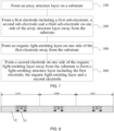
- FIG. 7 is a flowchart of a method for manufacturing a display panel according to an embodiment of the present disclosure. As shown in FIG. 7 , an embodiment of the present disclosure also provides a method for manufacturing a display panel, which is used for manufacturing the display panel according to any of the previous embodiments, and the method for manufacturing the display panel according to the embodiment of the present disclosure includes following acts.
- an array structure layer is formed on a substrate.
- the substrate includes a transistor.
- the transistor includes an active layer, a gate electrode, a source electrode, a drain electrode and a gate connecting electrode.
- the source electrode and the drain electrode are respectively connected with the active layer
- the gate connecting electrode is connected with the gate electrode through a conductive post.
- the transistor may be in a bottom gate structure or may be in a top gate structure.
- a first electrode including a first sub-electrode, a second sub-electrode and a third sub-electrode is formed on one side of the array structure layer away from the substrate.
- an organic light-emitting layer is formed on one side of the first electrode away from the substrate.
- a second electrode is formed on one side of the organic light-emitting layer away from the substrate to form a light-emitting structure layer including the first electrode, the organic light-emitting layer and a second electrode.
- the method for manufacturing the display panel in the embodiment of the present disclosure is used to manufacture the display panel according to any of the previous embodiments, and its implementation principle and implementation effect are similar, which is not repeated here.
- act 100 includes that: a transistor is formed on a substrate, a first insulating layer disposed with a first via hole is formed on the substrate on which the transistor is formed; a first conductive post is formed in the first via hole; a connecting electrode is formed on the first insulating layer; a second insulating layer disposed with a second via hole is formed on the first insulating layer formed with the connecting electrode; a second conductive post is formed in the second via hole.
- act 200 includes that: an anti-reflection thin film and photoresist are sequentially coated on one side of the array structure layer away from the substrate; exposing and developing processing of the anti-reflection thin film and the photoresist is performed; a first metal thin film and a second metal thin film are sequentially deposited on the anti-reflection thin film and the photoresist after exposuring processing; the substrate, on which the first metal thin film and the second metal thin film are deposited, is immersed in stripping solution to strip the photoresist; developing processing of the substrate stripped of the photoresist is performed to strip the anti-reflection thin film to form a third sub-electrode and a first sub-electrode; and a second sub-electrode is formed on one side of the first sub-electrode away from the substrate.
- an act where the second sub-electrode is formed on one side of the first sub-electrode away from the substrate includes that: a transparent conductive thin film is deposited on one side of the first sub-electrode away from the substrate by using a sputtering process; photoresist is coated on the transparent conductive thin film; exposing and developing processing of the photoresist is performed; the transparent conductive thin film is etched by using a dry etching process; the photoresist is stripped to form a second sub-electrode; an orthographic projection of the second sub-electrode on the substrate covers an orthographic projection of the first sub-electrode on the substrate.
- dry etching is used to form the second sub-electrode, which may ensure accuracy of the second sub-electrode.
- an interval time between a start time of depositing the transparent conductive thin film by using the sputtering process on one side of the first sub-electrode away from the substrate and an end time of immersing the substrate, on which the first metal thin film and the second metal thin film are deposited, in the stripping solution to strip the photoresist is less than 120 minutes to avoid oxidation corrosion of the first sub-electrode.
- the method for manufacturing the display panel further includes that: the substrate disposed with the array structure layer is cleaned.
- the method for manufacturing the display panel further includes that: dust attached onto the substrate on which the anti-reflection thin film and the photoresist are deposited is removed.
- coating the anti-reflection thin film before coating the photoresist may achieve purposes of enlarging a lithography process window and improving width control of a lithography strip.
- the anti-reflection thin film and the photoresist form a groove.
- the groove includes a first groove formed on the anti-reflection thin film and a second groove formed on the photoresist.
- An orthographic projection of the first groove on the substrate covers an orthographic projection of the second groove on the substrate, that is, the groove formed by the anti-reflection thin film and the photoresist is an undercut structure.
- a manufacturing material of the second metal thin film may be silver, and reflectivity of silver is as high as 95%, so the reflectivity of the first sub-electrode may be improved.
- a manufacturing material of the first metal thin film may be titanium.
- the substrate, on which the first metal thin film and the second metal thin film are deposited is immersed in the stripping solution for less than 30 minutes. This may avoid damage of the stripping solution to the second metal thin film, wherein the damage of the second metal thin film includes agglomeration damage or shrinkage of the second metal thin film.
- the method for manufacturing the display panel further includes that: a pixel definition thin film is deposited on one side of the first electrode away from the substrate; photoresist is coated on the pixel definition thin film; exposing and developing processing of the photoresist is performed; the pixel definition thin film is etched by using a dry etching process; the photoresist is stripped to form a pixel definition layer.
- the method for manufacturing the display panel further includes that: an encapsulating layer is formed on one side of the second electrode away from the substrate; a color filter layer is formed on one side of the encapsulating layer away from the substrate; a cover panel is formed on one side of the color filter layer away from the substrate.
- the “patterning process” in the present disclosure includes processing of film layer deposition, photoresist coating, mask exposure, development, etching, and photoresist stripping. Any one or more of sputtering, evaporation and chemical vapor deposition may be used for deposition, and any one or more of spray coating and spin coating may be used for coating.
- Thin film refers to a layer of thin film fabricated by a certain material on a base substrate by using a deposition or coating process.
- the "thin film” may also be referred to as a "layer”. If the "thin film” needs a patterning process throughout the whole manufacturing process, it is referred to as a "thin film” before the patterning process and as a "layer” after the patterning process.
- the "layer” after the patterning process contains at least one "pattern”.
- a substrate 10 is provided, and the substrate 10 includes a transistor 11.
- Transistors constitute a pixel driving circuit.
- the substrate 10 includes multiple sub-pixels, and each sub-pixel includes one pixel driving circuit, as shown in FIG. 8 .
- the display panel includes a display region and a non-display region, and sub-pixels are located in the display region.
- FIG. 8 three sub-pixels of the display region are illustrated: the first sub-pixel 100A, the second sub-pixel 100B and the third sub-pixel 100C, and the transistor 11 included in the pixel driving circuit is illustrated.
- source electrodes and drain electrodes of the display region are exposed on a surface of the substrate 10.
- a first insulating thin film is deposited on the substrate 10, and patterning of the first insulating thin film is performed by the patterning process to form a first insulating layer 12 covering the substrate 10, wherein the first insulating layer 12 forms multiple first vias, and the multiple first vias expose a drain electrode of each sub-pixel respectively.
- a first conductive post 13 is formed in the first via hole, and the first conductive post 13 is connected with the drain electrode of each sub-pixel.
- a conductive thin film is deposited on the first insulating layer 12, and patterning of the conductive thin film is performed by the patterning process to form a connecting electrode 14 with the first conductive post 13.
- a second insulating thin film is deposited on the connecting electrode 14, and patterning of the second insulating thin film is performed by the patterning process to form a second insulating layer 15 covering the substrate.
- the second insulating layer 15 forms multiple second vias, wherein the multiple second vias expose the connecting electrode 14 respectively, and second conductive posts 16 connected with the connecting electrode 14 are formed in the second vias to form an array structure layer, as shown in FIG. 9 .
- an anti-reflection thin film 200A and photoresist 200B are sequentially coated on the array structure layer, as shown in FIG. 10 .
- a manufacturing material of the anti-reflection thin film may be an organic material or an inorganic material.
- a layer of anti-reflection thin film is first coated before coating photoresist, which may achieve purposes of enlarging a lithography process window and improving width control of a lithography strip.
- the anti-reflection thin film 200A and the photoresist 200B are exposed by ultraviolet rays passing through a first mask M1. Be as shown in FIG. 11 .
- the anti-reflection thin film 200A and the photoresist 200B after developing processing are formed with a groove with an undercut structure.
- the groove includes a first groove formed on the anti-reflection thin film 200A after exposuring processing and a second groove formed on the photoresist 200B after exposuring processing.
- An orthographic projection of the first groove on the substrate 10 covers an orthographic projection of the second groove on the substrate 10.
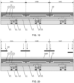
- a first metal thin film 210A and a second metal thin film 210B are sequentially deposited on the anti-reflection thin film 200A and the photoresist 200B after exposuring processing, as shown in FIG. 13 .
- the substrate 10, on which the first metal thin film 210A and the second metal thin film 210B are deposited is immersed in stripping solution to strip the photoresist 200B, wherein immersing time is less than 30 minutes, as shown in FIG. 14 .
- the second metal thin film 210B will be damaged and agglomerated, causing the second metal thin film 210B to fall off a surface of the first metal thin film 21 0A, or causing the second metal thin film 210B to shrink.
- act S8 developing processing of the anti-reflection thin film 200A is performed, and stripping of the anti-reflection thin film 200A is performed to form a third sub-electrode 213 and a first sub-electrode 211, as shown in FIG. 15 .
- a transparent conductive thin film 210C is deposited on the substrate formed with the first sub-electrode 211 by using a sputtering process, as shown in FIG. 16 .
- a time interval between an end time of act S7 and a start time of act S9 is less than 120 minutes, so as to prevent the first sub-electrode 211 from being blackened by oxidation corrosion.
- photoresist 200B is coated on the transparent conductive thin film 210C, and exposing processing of the photoresist 200B is performed by ultraviolet rays passing through a second mask M2, as shown in FIG. 17 .
- act S11 developing processing of the photoresist 200B after exposuring processing is performed, the transparent conductive thin film 210C is etched by using a dry etching process, and the photoresist is stripped to form a second sub-electrode 212 to form a first electrode 21, as shown in FIG. 18 .
- a pixel definition thin film 240 is deposited on the substrate formed with the first electrode by using Plasma Enhanced Chemical Vapor Deposition (PECVD), as shown in FIG. 19 .
- PECVD Plasma Enhanced Chemical Vapor Deposition
- photoresist 200B is coated on the pixel definition thin film 240, and exposing processing of the photoresist 200B is performed by ultraviolet rays passing through a second mask M3, as shown in FIG. 20 .
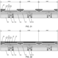
- act S14 developing processing of the photoresist 200B after exposuring processing, the pixel definition thin film 240 is etched by using the dry etching process, and the photoresist is stripped to form the pixel definition layer 24, as shown in FIG. 21 .
- the pixel definition layer 24 is opened with a pixel opening, and the pixel opening exposes a surface of the first electrode 21.
- an organic light-emitting layer 22 and a second electrode 23 are sequentially formed on the substrate on which the pixel definition layer is formed, as shown in FIG. 22 .
- the organic light-emitting layer 22 is electrically connected with the first electrode 21, and the second electrode 23 is electrically connected with the organic light-emitting layer 22.
- a first encapsulating thin film is deposited on the second electrode 23, and the first encapsulating thin film is patterned by a patterning process to form a first encapsulating layer 251; a second encapsulating thin film is deposited on the first encapsulating layer 251, and the second encapsulating thin film is patterned by a patterning process to form a second encapsulating layer 252; a third encapsulating thin film is coated on the second encapsulating layer 252, and the third encapsulating thin film is patterned by mask, exposure and development processes to form a third encapsulating layer 253 to form an encapsulating layer 25, as shown in FIG. 23 .
- a color filter layer 30 is formed on one side of the encapsulating layer 25 away from the substrate, as shown in FIG. 5 .
- the color filter layer 30 includes a first color filter, a second color filter and a third color filter corresponding to sub-pixels.
- the first color filter may be a green (G) color filter
- the second color filter may be a red (R) color filter
- the third color filter may be a blue (B) color filter.
- a process of preparing the color filter layer 30 includes the blue (B) color filter is first formed, the red (R) color filter is then formed, and the green (G) color filter is then formed. Adhesion of the blue filter is relatively high, and first forming the blue filter first may reduce possibility of stripping the color filter layer 30 from the thin film layer in contact with the color filter layer.
- the red filter has relatively small adhesion but good fluidity, in a process of forming the red filter R, a quantity of bubbles of surfaces of the blue filter and the red filter away from one side of the second electrode may be reduced, so that uniformity of film thickness at an overlapping position of the blue filter and the red filter may be improved. Since a base material of the green filter is approximately the same as that of the red filter, adhesion between the green filter and the red filter is relative large, which may reduce possibility of stripping the color filter layer 30 from the second electrode.
- the color filter layer 30 may include a filter of another color, such as white or yellow.
- a cover panel 40 is formed by using a sealing process, and the cover panel 40 and the substrate 10 are fixed by sealant (not shown in the figure), as shown in FIG. 6 .
- An embodiment of the present disclosure also provides an electronic device, including the display panel according to any one of the previous embodiments.
- the electronic device includes a VR device or an AR device.
Landscapes
- Engineering & Computer Science (AREA)
- Microelectronics & Electronic Packaging (AREA)
- Manufacturing & Machinery (AREA)
- Physics & Mathematics (AREA)
- Optics & Photonics (AREA)
- Electroluminescent Light Sources (AREA)
- Devices For Indicating Variable Information By Combining Individual Elements (AREA)
Applications Claiming Priority (1)
| Application Number | Priority Date | Filing Date | Title |
|---|---|---|---|
| PCT/CN2020/081837 WO2021189473A1 (zh) | 2020-03-27 | 2020-03-27 | 显示面板及其制作方法、电子设备 |
Publications (2)
| Publication Number | Publication Date |
|---|---|
| EP4131396A1 true EP4131396A1 (de) | 2023-02-08 |
| EP4131396A4 EP4131396A4 (de) | 2023-05-24 |
Family
ID=77891497
Family Applications (1)
| Application Number | Title | Priority Date | Filing Date |
|---|---|---|---|
| EP20900759.0A Pending EP4131396A4 (de) | 2020-03-27 | 2020-03-27 | Anzeigetafel, verfahren zur herstellung davon und elektronische vorrichtung |
Country Status (5)
| Country | Link |
|---|---|
| US (1) | US20220115468A1 (de) |
| EP (1) | EP4131396A4 (de) |
| JP (1) | JP2023528700A (de) |
| CN (1) | CN113748516A (de) |
| WO (1) | WO2021189473A1 (de) |
Families Citing this family (6)
| Publication number | Priority date | Publication date | Assignee | Title |
|---|---|---|---|---|
| CN115735184B (zh) * | 2020-03-18 | 2025-06-17 | 京东方科技集团股份有限公司 | 显示面板及显示装置 |
| TWI756680B (zh) * | 2020-05-06 | 2022-03-01 | 友達光電股份有限公司 | 顯示裝置 |
| CN114050222B (zh) * | 2021-11-16 | 2025-03-07 | 京东方科技集团股份有限公司 | 显示基板、显示基板的制作方法和显示装置 |
| CN115457863B (zh) * | 2022-09-15 | 2025-05-27 | 北京京东方技术开发有限公司 | 显示面板及其衬底基板的对位方法、电子设备 |
| CN116682330B (zh) * | 2023-06-19 | 2024-07-16 | 科睿者科技(深圳)有限公司 | 一种透明显示面板及显示设备 |
| CN119677344B (zh) * | 2024-12-17 | 2025-10-10 | 南京昀光科技有限公司 | 一种显示面板及其制备方法、显示装置 |
Family Cites Families (27)
| Publication number | Priority date | Publication date | Assignee | Title |
|---|---|---|---|---|
| US5994174A (en) * | 1997-09-29 | 1999-11-30 | The Regents Of The University Of California | Method of fabrication of display pixels driven by silicon thin film transistors |
| US6013538A (en) * | 1997-11-24 | 2000-01-11 | The Trustees Of Princeton University | Method of fabricating and patterning OLEDs |
| JP2002246185A (ja) * | 2001-02-22 | 2002-08-30 | Victor Co Of Japan Ltd | 有機エレクトロルミネセンス素子 |
| JP4461726B2 (ja) * | 2003-07-16 | 2010-05-12 | ソニー株式会社 | 有機発光素子およびその製造方法、ならびに表示装置 |
| JP2005285395A (ja) * | 2004-03-29 | 2005-10-13 | Fujitsu Display Technologies Corp | 配線構造並びにそれを備えた表示装置用基板及び表示装置 |
| KR100667082B1 (ko) * | 2005-11-02 | 2007-01-10 | 삼성에스디아이 주식회사 | 유기전계발광소자 및 그 제조방법 |
| JP5235011B2 (ja) * | 2009-11-16 | 2013-07-10 | 株式会社神戸製鋼所 | 有機elディスプレイ用の反射アノード電極 |
| US9620560B2 (en) * | 2011-08-26 | 2017-04-11 | Joled Inc. | EL display device and method for manufacturing same |
| JP2013054863A (ja) * | 2011-09-01 | 2013-03-21 | Sony Corp | 有機el表示装置、有機el表示装置の製造方法および電子機器 |
| CN103137441A (zh) * | 2011-11-22 | 2013-06-05 | 上海华虹Nec电子有限公司 | 半导体工艺中制作细长型孤立线条图形的方法 |
| KR101951223B1 (ko) * | 2012-10-26 | 2019-02-25 | 삼성디스플레이 주식회사 | 표시장치 및 그 제조방법 |
| US9553156B2 (en) * | 2014-07-16 | 2017-01-24 | Lg Display Co., Ltd. | Organic light emitting display device and method of manufacturing the same |
| KR102540372B1 (ko) * | 2015-05-28 | 2023-06-05 | 엘지디스플레이 주식회사 | 유기 발광 표시 장치 및 그 제조 방법 |
| KR101795579B1 (ko) * | 2015-11-10 | 2017-11-08 | 엘지디스플레이 주식회사 | 유기 발광 표시 장치 및 그 제조 방법 |
| KR102630001B1 (ko) * | 2016-10-31 | 2024-01-25 | 엘지디스플레이 주식회사 | 유기발광 표시장치, 그를 포함한 헤드 장착형 디스플레이, 및 그의 제조방법 |
| US20180151830A1 (en) * | 2016-11-30 | 2018-05-31 | Canon Kabushiki Kaisha | Display device and electronic device |
| JP6975543B2 (ja) * | 2017-03-29 | 2021-12-01 | ジオマテック株式会社 | 有機エレクトロルミネッセンス素子用電極、有機エレクトロルミネッセンス素子、有機エレクトロルミネッセンス表示装置、及び有機エレクトロルミネッセンス素子用電極の製造方法 |
| KR102325674B1 (ko) * | 2017-08-16 | 2021-11-12 | 엘지디스플레이 주식회사 | 유기발광 표시장치, 그를 포함한 헤드 장착형 디스플레이, 및 그의 제조방법 |
| JP7182908B2 (ja) * | 2018-06-18 | 2022-12-05 | 東京エレクトロン株式会社 | 有機elパネル、および有機elパネルの製造方法 |
| CN109378395B (zh) * | 2018-10-18 | 2021-08-06 | 京东方科技集团股份有限公司 | 纳米粒子、显示基板的制备方法及显示装置 |
| CN109713026B (zh) * | 2019-02-26 | 2024-09-20 | 京东方科技集团股份有限公司 | 一种硅基电致发光显示面板及其制造方法、显示装置 |
| CN112492890B (zh) * | 2019-07-12 | 2025-02-07 | 京东方科技集团股份有限公司 | 显示基板及其制备方法、显示装置 |
| CN110459699B (zh) * | 2019-08-30 | 2022-07-15 | 京东方科技集团股份有限公司 | 显示基板及其制备方法、显示装置 |
| CN110610975B (zh) * | 2019-09-23 | 2022-04-08 | 京东方科技集团股份有限公司 | 显示基板及其制备方法、显示装置 |
| CN110610980B (zh) * | 2019-10-23 | 2022-06-03 | 京东方科技集团股份有限公司 | 一种显示基板及其制备方法、显示装置 |
| KR102854144B1 (ko) * | 2019-12-30 | 2025-09-02 | 엘지디스플레이 주식회사 | 투명 표시 장치 |
| CN114946093A (zh) * | 2020-01-08 | 2022-08-26 | 索尼集团公司 | 发光元件及其制造方法和发光元件阵列 |
-
2020
- 2020-03-27 EP EP20900759.0A patent/EP4131396A4/de active Pending
- 2020-03-27 US US17/264,290 patent/US20220115468A1/en not_active Abandoned
- 2020-03-27 WO PCT/CN2020/081837 patent/WO2021189473A1/zh not_active Ceased
- 2020-03-27 JP JP2021570498A patent/JP2023528700A/ja active Pending
- 2020-03-27 CN CN202080000405.9A patent/CN113748516A/zh active Pending
Also Published As
| Publication number | Publication date |
|---|---|
| EP4131396A4 (de) | 2023-05-24 |
| JP2023528700A (ja) | 2023-07-06 |
| CN113748516A (zh) | 2021-12-03 |
| US20220115468A1 (en) | 2022-04-14 |
| WO2021189473A1 (zh) | 2021-09-30 |
Similar Documents
| Publication | Publication Date | Title |
|---|---|---|
| EP4131396A1 (de) | Anzeigetafel, verfahren zur herstellung davon und elektronische vorrichtung | |
| JP7525512B2 (ja) | 表示基板及びその製造方法、表示装置 | |
| WO2021233002A1 (zh) | 显示基板及其制作方法、显示装置 | |
| CN116156957B (zh) | 显示基板及其制备方法、显示装置 | |
| US12016232B2 (en) | Display substrate and preparation method thereof, and display apparatus | |
| US11475837B2 (en) | Silicon-based organic light-emitting diode display device and silicon-based organic light-emitting diode display method | |
| JP7547384B2 (ja) | 表示基板及びその製造方法、表示装置 | |
| US11968879B2 (en) | Display substrate, manufacturing method thereof, and display apparatus | |
| CN215988833U (zh) | 显示基板和显示装置 | |
| CN117652226B (zh) | 显示基板及其制备方法、显示装置 | |
| US12219795B2 (en) | Display substrate, preparation method thereof, and display device | |
| WO2025065269A1 (zh) | 一种显示基板及其制作方法、显示装置 |
Legal Events
| Date | Code | Title | Description |
|---|---|---|---|
| STAA | Information on the status of an ep patent application or granted ep patent |
Free format text: STATUS: UNKNOWN |
|
| STAA | Information on the status of an ep patent application or granted ep patent |
Free format text: STATUS: THE INTERNATIONAL PUBLICATION HAS BEEN MADE |
|
| PUAI | Public reference made under article 153(3) epc to a published international application that has entered the european phase |
Free format text: ORIGINAL CODE: 0009012 |
|
| STAA | Information on the status of an ep patent application or granted ep patent |
Free format text: STATUS: REQUEST FOR EXAMINATION WAS MADE |
|
| 17P | Request for examination filed |
Effective date: 20210625 |
|
| AK | Designated contracting states |
Kind code of ref document: A1 Designated state(s): AL AT BE BG CH CY CZ DE DK EE ES FI FR GB GR HR HU IE IS IT LI LT LU LV MC MK MT NL NO PL PT RO RS SE SI SK SM TR |
|
| REG | Reference to a national code |
Ref country code: DE Ref legal event code: R079 Free format text: PREVIOUS MAIN CLASS: H01L0027320000 Ipc: H10K0059123000 |
|
| A4 | Supplementary search report drawn up and despatched |
Effective date: 20230420 |
|
| RIC1 | Information provided on ipc code assigned before grant |
Ipc: H10K 102/00 20230101ALN20230414BHEP Ipc: H10K 59/80 20230101ALI20230414BHEP Ipc: H10K 59/123 20230101AFI20230414BHEP |
|
| DAV | Request for validation of the european patent (deleted) | ||
| DAX | Request for extension of the european patent (deleted) |