EP4131403A1 - Anzeigetafel und flexible anzeigevorrichtung - Google Patents
Anzeigetafel und flexible anzeigevorrichtung Download PDFInfo
- Publication number
- EP4131403A1 EP4131403A1 EP20928317.5A EP20928317A EP4131403A1 EP 4131403 A1 EP4131403 A1 EP 4131403A1 EP 20928317 A EP20928317 A EP 20928317A EP 4131403 A1 EP4131403 A1 EP 4131403A1
- Authority
- EP
- European Patent Office
- Prior art keywords
- layer
- substrate
- display panel
- area
- disposed
- Prior art date
- Legal status (The legal status is an assumption and is not a legal conclusion. Google has not performed a legal analysis and makes no representation as to the accuracy of the status listed.)
- Pending
Links
Images



Classifications
-
- G—PHYSICS
- G09—EDUCATION; CRYPTOGRAPHY; DISPLAY; ADVERTISING; SEALS
- G09F—DISPLAYING; ADVERTISING; SIGNS; LABELS OR NAME-PLATES; SEALS
- G09F9/00—Indicating arrangements for variable information in which the information is built-up on a support by selection or combination of individual elements
- G09F9/30—Indicating arrangements for variable information in which the information is built-up on a support by selection or combination of individual elements in which the desired character or characters are formed by combining individual elements
- G09F9/301—Indicating arrangements for variable information in which the information is built-up on a support by selection or combination of individual elements in which the desired character or characters are formed by combining individual elements flexible foldable or roll-able electronic displays, e.g. thin LCD, OLED
-
- B—PERFORMING OPERATIONS; TRANSPORTING
- B32—LAYERED PRODUCTS
- B32B—LAYERED PRODUCTS, i.e. PRODUCTS BUILT-UP OF STRATA OF FLAT OR NON-FLAT, e.g. CELLULAR OR HONEYCOMB, FORM
- B32B27/00—Layered products comprising a layer of synthetic resin
- B32B27/28—Layered products comprising a layer of synthetic resin comprising synthetic resins not wholly covered by any one of the sub-groups B32B27/30 - B32B27/42
- B32B27/283—Layered products comprising a layer of synthetic resin comprising synthetic resins not wholly covered by any one of the sub-groups B32B27/30 - B32B27/42 comprising polysiloxanes
-
- B—PERFORMING OPERATIONS; TRANSPORTING
- B32—LAYERED PRODUCTS
- B32B—LAYERED PRODUCTS, i.e. PRODUCTS BUILT-UP OF STRATA OF FLAT OR NON-FLAT, e.g. CELLULAR OR HONEYCOMB, FORM
- B32B3/00—Layered products comprising a layer with external or internal discontinuities or unevennesses, or a layer of non-planar shape; Layered products comprising a layer having particular features of form
- B32B3/26—Layered products comprising a layer with external or internal discontinuities or unevennesses, or a layer of non-planar shape; Layered products comprising a layer having particular features of form characterised by a particular shape of the outline of the cross-section of a continuous layer; characterised by a layer with cavities or internal voids ; characterised by an apertured layer
- B32B3/266—Layered products comprising a layer with external or internal discontinuities or unevennesses, or a layer of non-planar shape; Layered products comprising a layer having particular features of form characterised by a particular shape of the outline of the cross-section of a continuous layer; characterised by a layer with cavities or internal voids ; characterised by an apertured layer characterised by an apertured layer, the apertures going through the whole thickness of the layer, e.g. expanded metal, perforated layer, slit layer regular cells B32B3/12
-
- B—PERFORMING OPERATIONS; TRANSPORTING
- B32—LAYERED PRODUCTS
- B32B—LAYERED PRODUCTS, i.e. PRODUCTS BUILT-UP OF STRATA OF FLAT OR NON-FLAT, e.g. CELLULAR OR HONEYCOMB, FORM
- B32B7/00—Layered products characterised by the relation between layers; Layered products characterised by the relative orientation of features between layers, or by the relative values of a measurable parameter between layers, i.e. products comprising layers having different physical, chemical or physicochemical properties; Layered products characterised by the interconnection of layers
- B32B7/04—Interconnection of layers
- B32B7/12—Interconnection of layers using interposed adhesives or interposed materials with bonding properties
-
- G—PHYSICS
- G06—COMPUTING OR CALCULATING; COUNTING
- G06F—ELECTRIC DIGITAL DATA PROCESSING
- G06F1/00—Details not covered by groups G06F3/00 - G06F13/00 and G06F21/00
- G06F1/16—Constructional details or arrangements
- G06F1/1613—Constructional details or arrangements for portable computers
- G06F1/1633—Constructional details or arrangements of portable computers not specific to the type of enclosures covered by groups G06F1/1615 - G06F1/1626
- G06F1/1637—Details related to the display arrangement, including those related to the mounting of the display in the housing
-
- G—PHYSICS
- G06—COMPUTING OR CALCULATING; COUNTING
- G06F—ELECTRIC DIGITAL DATA PROCESSING
- G06F1/00—Details not covered by groups G06F3/00 - G06F13/00 and G06F21/00
- G06F1/16—Constructional details or arrangements
- G06F1/1613—Constructional details or arrangements for portable computers
- G06F1/1633—Constructional details or arrangements of portable computers not specific to the type of enclosures covered by groups G06F1/1615 - G06F1/1626
- G06F1/1637—Details related to the display arrangement, including those related to the mounting of the display in the housing
- G06F1/1641—Details related to the display arrangement, including those related to the mounting of the display in the housing the display being formed by a plurality of foldable display components
-
- G—PHYSICS
- G06—COMPUTING OR CALCULATING; COUNTING
- G06F—ELECTRIC DIGITAL DATA PROCESSING
- G06F1/00—Details not covered by groups G06F3/00 - G06F13/00 and G06F21/00
- G06F1/16—Constructional details or arrangements
- G06F1/1613—Constructional details or arrangements for portable computers
- G06F1/1633—Constructional details or arrangements of portable computers not specific to the type of enclosures covered by groups G06F1/1615 - G06F1/1626
- G06F1/1637—Details related to the display arrangement, including those related to the mounting of the display in the housing
- G06F1/1652—Details related to the display arrangement, including those related to the mounting of the display in the housing the display being flexible, e.g. mimicking a sheet of paper, or rollable
-
- G—PHYSICS
- G06—COMPUTING OR CALCULATING; COUNTING
- G06F—ELECTRIC DIGITAL DATA PROCESSING
- G06F3/00—Input arrangements for transferring data to be processed into a form capable of being handled by the computer; Output arrangements for transferring data from processing unit to output unit, e.g. interface arrangements
- G06F3/01—Input arrangements or combined input and output arrangements for interaction between user and computer
- G06F3/03—Arrangements for converting the position or the displacement of a member into a coded form
- G06F3/041—Digitisers, e.g. for touch screens or touch pads, characterised by the transducing means
- G06F3/0412—Digitisers structurally integrated in a display
-
- G—PHYSICS
- G09—EDUCATION; CRYPTOGRAPHY; DISPLAY; ADVERTISING; SEALS
- G09F—DISPLAYING; ADVERTISING; SIGNS; LABELS OR NAME-PLATES; SEALS
- G09F9/00—Indicating arrangements for variable information in which the information is built-up on a support by selection or combination of individual elements
- G09F9/30—Indicating arrangements for variable information in which the information is built-up on a support by selection or combination of individual elements in which the desired character or characters are formed by combining individual elements
- G09F9/33—Indicating arrangements for variable information in which the information is built-up on a support by selection or combination of individual elements in which the desired character or characters are formed by combining individual elements being semiconductor devices, e.g. diodes
-
- B—PERFORMING OPERATIONS; TRANSPORTING
- B32—LAYERED PRODUCTS
- B32B—LAYERED PRODUCTS, i.e. PRODUCTS BUILT-UP OF STRATA OF FLAT OR NON-FLAT, e.g. CELLULAR OR HONEYCOMB, FORM
- B32B2307/00—Properties of the layers or laminate
- B32B2307/40—Properties of the layers or laminate having particular optical properties
- B32B2307/42—Polarizing, birefringent, filtering
-
- B—PERFORMING OPERATIONS; TRANSPORTING
- B32—LAYERED PRODUCTS
- B32B—LAYERED PRODUCTS, i.e. PRODUCTS BUILT-UP OF STRATA OF FLAT OR NON-FLAT, e.g. CELLULAR OR HONEYCOMB, FORM
- B32B2457/00—Electrical equipment
- B32B2457/20—Displays, e.g. liquid crystal displays, plasma displays
- B32B2457/208—Touch screens
-
- H—ELECTRICITY
- H04—ELECTRIC COMMUNICATION TECHNIQUE
- H04M—TELEPHONIC COMMUNICATION
- H04M1/00—Substation equipment, e.g. for use by subscribers
- H04M1/02—Constructional features of telephone sets
- H04M1/0202—Portable telephone sets, e.g. cordless phones, mobile phones or bar type handsets
- H04M1/0206—Portable telephones comprising a plurality of mechanically joined movable body parts, e.g. hinged housings
- H04M1/0208—Portable telephones comprising a plurality of mechanically joined movable body parts, e.g. hinged housings characterized by the relative motions of the body parts
- H04M1/0214—Foldable telephones, i.e. with body parts pivoting to an open position around an axis parallel to the plane they define in closed position
-
- H—ELECTRICITY
- H04—ELECTRIC COMMUNICATION TECHNIQUE
- H04M—TELEPHONIC COMMUNICATION
- H04M1/00—Substation equipment, e.g. for use by subscribers
- H04M1/02—Constructional features of telephone sets
- H04M1/0202—Portable telephone sets, e.g. cordless phones, mobile phones or bar type handsets
- H04M1/026—Details of the structure or mounting of specific components
- H04M1/0266—Details of the structure or mounting of specific components for a display module assembly
- H04M1/0268—Details of the structure or mounting of specific components for a display module assembly including a flexible display panel
-
- Y—GENERAL TAGGING OF NEW TECHNOLOGICAL DEVELOPMENTS; GENERAL TAGGING OF CROSS-SECTIONAL TECHNOLOGIES SPANNING OVER SEVERAL SECTIONS OF THE IPC; TECHNICAL SUBJECTS COVERED BY FORMER USPC CROSS-REFERENCE ART COLLECTIONS [XRACs] AND DIGESTS
- Y02—TECHNOLOGIES OR APPLICATIONS FOR MITIGATION OR ADAPTATION AGAINST CLIMATE CHANGE
- Y02E—REDUCTION OF GREENHOUSE GAS [GHG] EMISSIONS, RELATED TO ENERGY GENERATION, TRANSMISSION OR DISTRIBUTION
- Y02E10/00—Energy generation through renewable energy sources
- Y02E10/50—Photovoltaic [PV] energy
- Y02E10/549—Organic PV cells
Definitions
- the present disclosure relates to the field of display technology, and more particularly, to a display panel and a flexible display device.
- the flexible display device has been widely applied to various fields due to its excellent flexibility and bendability. Compared with traditional screens, the advantages of flexible screens are more obvious. For a flexible display device, to achieve its flexible folding function, the screen itself must have better bending ability and flat performance. Moreover, in order to ensure the folding performance of the entire device, the folding performance of other components matching the screen should also be good.
- conventional flexible display device generally comprises a plurality of supporting backplanes and adhesive layers, making the thickness thicker. The flexible display device with great thickness is not only inconvenient to carry, but also adversely affects the bending of the flexible device.
- the dislocation of the glue layers between each of the film layers of the screen is not consistent with the dislocation of each of the film layers, and the tearing problem between the glue layer and the film layer is likely to occur, which may damage the screen and affect the display effect.
- the rigidity and strength of some film layers are too high.
- the stress concentrated at the transition point of the water drop is not conducive to enhance the overall performance of the flexible display device.
- the conventional flexible display device with great thickness is inconvenient to carry and use. Moreover, when the device is bent or folded, the layers between each of the film layers are easily torn, and the screen is damaged. Further, the high rigidity and strength of each film layer of the device are not conducive to enhance the overall performance of the flexible display device.
- the present disclosure provides a display panel and a flexible display device to solve the problems of the conventional flexible display device, which is thick, not portable and not easily used. Moreover, the present disclosure solves the tearing problem of the layers between each of the film layers, and the damage problem of the screen when the device is bent or folded. Moreover, the present disclosure solves the problem that is not conducive to the enhancement of the overall performance of flexible display device due to the higher rigidity and strength of each film layer of the device.
- the present disclosure provides a display panel, comprising:
- the substrate comprises at least one of a bending area, a straight area, and a connection area, and the bending area is connected to the straight area through the connection area.
- the substrate further comprises a first grid structure and a second grid structure.
- the first grid structure is disposed on the bending area of the substrate, and the second grid structure is disposed on connection area of the substrate.
- a shape of the first grid structure is the same as a shape of the second grid structure.
- a radial length of the first grid structure is greater than a radial length of the second grid structure.
- a shape of each of the plurality of grid structures comprises a strip shape, a circular shape, an elliptical shape, or a wave shape.
- the plurality of grid structures are arranged in an array manner.
- the present disclosure provides a display panel, comprising:
- the substrate comprises at least one of a bending area, a straight area, and a connection area, and the bending area is connected to the straight area through the connection area.
- the substrate further comprises a first grid structure and a second grid structure.
- the first grid structure is disposed on the bending area of the substrate, and the second grid structure is disposed on connection area of the substrate.
- a shape of the first grid structure is the same as a shape of the second grid structure.
- a density of the first grid structure is greater than a density of the second grid structure.
- a radial length of the first grid structure is greater than a radial length of the second grid structure.
- a density of the plurality of the grid structures in the connection area gradually decreases along the bending area toward the straight area.
- each of the plurality of the grid structures penetrates the substrate.
- two lateral sides of the substrate comprise a plurality of openings arranged at equal intervals.
- a shape of each of the plurality of grid structures comprises a strip shape, a circular shape, an elliptical shape, or a wave shape.
- the plurality of grid structures are arranged in an array manner.
- At least one edge of the grid structure in the length direction is an arc shape.
- the display layer further comprises a touch layer and a polarizer.
- the touch layer is disposed on the light-emitting device layer, and the polarizer is disposed on the touch layer.
- the display panel further comprises an elastic layer.
- the elastic layer is disposed in the same layer as the substrate, and the elastic layer fills each of the plurality of grid structures.
- a material of the elastic layer comprises silicone resin, metal material or amorphous material.
- the present disclosure further provides a flexible display device, comprising:
- the present disclosure provides a display panel and a flexible display device.
- the substrate of the display panel in the embodiments of the present disclosure is arranged into a bending area, a straight area, and a connection area.
- a plurality of discontinuous grid structures are disposed on the substrate corresponding to the bending area and the connection area.
- the display panel of the embodiments of the present disclosure does not require a backplane layer and a pressure-sensitive adhesive layer, resulting in a light and thin overall structure of the panel.
- the panel may be easily and conveniently carried when bent and provides excellent overall performance.
- the flexible display device may be bent or folded during use to achieve the requirements of diverse function of the flexible display device.
- the bending or folding performance of the flexible display device is related to various factors, such as the thickness of the display device.
- the conventional flexible display device is generally thick. When the device is folded or bent, the dislocations between the film layers are not consistent, resulting in many problems, which are not conducive to enhance the overall performance of the display device.
- a display panel and a flexible display device are provided.
- FIG. 1 is a schematic diagram of each layer of the display panel according to one embodiment of the present disclosure.
- the display panel comprises a substrate 100, a first adhesive layer 101, a display layer 102, a second adhesive layer 103, and a protective layer 104.
- the first adhesive layer 101 is disposed on the substrate 100
- the display layer 102 is disposed on the substrate 100
- the display layer 102 is adhered to the substrate 100 through the first adhesive layer 101
- the second adhesive layer 103 is disposed on the display layer 102.
- the protective layer 104 is disposed on the display layer 102, and the protective layer 104 is adhered to the display layer 102 through the second adhesive layer 103.
- the first adhesive layer 101 and the second adhesive layer 102 may be adhesive layers commonly used in manufacturing the display panels, such as optically clear adhesives (OCA), and the capacitive type OCA or resistive type OCA may be selected according to various requirements of different display panels.
- OCA optically clear adhesives
- the capacitive type OCA or resistive type OCA may be selected according to various requirements of different display panels.
- both the substrate 100 and the display layer 102 are tightly adhered to the first adhesive layer 101, and the display layer 102 and the protective layer 104 are tightly adhered to the second adhesive layer 103.
- the first adhesive layer 101 and the second adhesive layer 103 are shifted consistently with other film layers to ensure desirable bending or folding performance of the panel, and effectively prevent the adhesive layer from being misaligned and torn.
- the materials of the first adhesive layer 101 and the second adhesive layer 103 may be the same.
- the display layer 102 is a normal display function layer of the display panel.
- the display layer 102 may be disposed according to a conventional manufacturing process and a conventional film layer.
- the display layer 102 provides a display screen of the screen and ensures the normal light-emitting display of the panel.
- the display layer 102 comprises an array layer and a light-emitting device layer.
- the light emitting device layer is disposed on the array layer.
- the array layer of the display layer 102 is directly formed on the substrate 100, and the array layer is directly adhered to the substrate 100 through the first adhesive layer 101. That is, no any other film layer, such as a backplane layer, is disposed between the substrate 100 and the array layer.
- the display layer 102 is directly supported by the substrate 100, thereby reducing the film structure of the flexible display device and making the flexible display device lighter and thinner.
- the substrate 100 may be a supporting layer, which is used to support the display layer 102 and other film layers thereon.
- the light-emitting device layer further comprises film layer structures, such as an anode layer, a light-emitting layer, and a cathode layer. These film layer structures may be disposed on the array layer according to the process of a conventional display panel, which is not described in detail any more.
- the display layer 102 may further comprise a touch layer and a polarizer.
- the touch layer is disposed on the light-emitting device layer, and the polarizer is disposed on the touch layer, to achieve the display and touch functions of the display panel.
- the substrate 100 disclosed in the embodiment of the present disclosure is directly adhered to the display layer 102 through the first adhesive layer 101.
- the backplane layer and the pressure-sensitive adhesive layer adhered to the backplane layer are no longer disposed. Therefore, the overall thickness of the display panel is effectively reduced, allowing the display panel to become thinner, and the bending performance is improved when the device is bent or folded.
- the display panel in the embodiment of the present disclosure removes the backplane layer and the pressure-sensitive adhesive layer.
- the influence of the backplane layer and the pressure-sensitive adhesive layer on the panel is correspondingly reduced, and the tearing problem of the film layers is effectively improved.
- FIG. 2 is a schematic plan view of the substrate according to one embodiment of the present disclosure.
- the substrate 100 of the embodiment of the present disclosure comprises a straight area 201, a connection area 202, and a bending are 203.
- the straight area 201 is connected to the bending area 203 through the connection area 202.
- the substrate 100 may comprise a plurality of different areas described above.
- the substrate 100 is generally a steel plate or a hard material
- the preferred bending state of the bending portion is a water drop shape or a water drop-like shape. Under this state, the stress level and bending performance of the bending portion of the panel are good. Therefore, when the structure of each film layer and the structure of the substrate of the panel is designed, it is ensured that the shape of the bending portion forms a drop shape or a water drop-like shape after bending.
- the substrate 100 of the embodiment of the present disclosure bends as the display panel bends.
- the connection area 202 and the bending area 203 are bent.
- the connection area 202 mainly has a transitional function. After bending, the connection area 202 and the bending area 203 form a water drop shape, and the stress concentrated in the connection area 202 is obvious, especially the stress near the bending area 203 is greatest.
- connection areas 202 are symmetrically distributed with respect to the bending areas 203, and are connected to two lateral sides of the straight area 201.
- the substrate 100 of the embodiment of the present disclosure comprises a plurality of grid structures arranged discontinuously.
- a first grid structure is disposed on the bending area 203, and a second grid structure is disposed on the connection area 202.
- the grid structures make the bending of the substrate easier and enhance the flexibility of the substrate.
- FIG. 3A is a schematic bending view of the display panel according to one embodiment of the present disclosure.
- the display panel 300 comprises a substrate 301 and other film layers connected to the substrate 301.
- the structures of the other film layers are shown in FIG. 1 and would not be described in detail herein.
- the straight area 302 of the substrate 301 remains straight, the bending area 304 is deformed the most, and the connection area 303 is deformed to a certain extent. Meanwhile, when the bending area 304 and the connecting area 303 form a water drop shape or a water drop-like shape, the bending effect of the display panel 300 is the best.
- the shape of the first grid structure and the shape of the second grid structure may be the same or different.
- the first grid structure and the second grid structure with the same shape are used as an example for description.
- FIG. 3B is a schematic view of the substrate according to one embodiment of the present disclosure.
- the substrate 30 comprises a straight area 31, a connection area 32, and a bending area 33.
- the straight area 31 is connected to the bending area 33 through the connection area 32, and a first grid structure 35 is disposed on the bending area 33, and a second grid structure 34 is disposed on the connection area 32.
- No any grid structure is disposed on the substrate 100 corresponding to the straight area 31.
- the shape and disposed manner of the first grid structure 35 and the second grid structure 35 may be the same or different, and specifically, are disposed according to actual products.
- the deformation area mainly occurs in the connection area 32 and the bending area 33.
- the first grid structure 35 and the second grid structure 34 in the area are deformed.
- the grid structure is elongated or compressed, so that the substrate 100 is more easily bent.
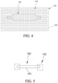
- FIG. 4 is a schematic view of the grid structures in the bending area of the substrate according to one embodiment of the present disclosure.
- a plurality of the first grids 401 are discontinuously formed on the hollow substrate 400.
- the plurality of the first grids 401 may be arranged in a regular array.
- the length and width of the substrate in the bending area are disposed at equal intervals.
- the shape, structure and size of each of the first grids 401 may be disposed to be the same or different. In the present embodiment, in order to simplify the manufacturing process, each of the first grids 401 is disposed the same.
- the length direction of the first grid 401 is parallel to the bending direction.
- the substrate 400 When the bending area is bent, since the first grid 401 is disposed on the bending area of the substrate 400, little physical connection material is disposed between the grids, thereby increasing the flexibility of the substrate 400.
- the force applied the substrate 400 is the same as the force applied to a conventional substrate, the substrate 400 may be bent easily, and the bending degree of the substrate 400 is great.
- the stretching area 403 is subjected to a bending stretching stress, the grid structures in the stretching area 403 may be deformed in both of the length or width directions, and adjacent grids are connected by the substrate 400.
- the first grid is dense, little physical material is disposed between the connected grids, and it is easier to bend and deform without breaking. Thereby, the bending performance of the substrate 400 is enhanced, and the bending or folding performance of the display panel is enhanced.
- the openings 402 are further disposed on both lateral sides of the substrate 400.
- the opening 402 is part of the first grid 401.
- the distance between adjacent openings 402 is the same, and the openings 402 make the substrate 400 more flexible.
- the width of the opening 402 may be the same as the width of the first grid 401 or greater than the width of the first grid 401.
- FIG. 5 is a schematic view of the first grid structure according to one embodiment of the present disclosure.
- the first grid 401 comprises a first area 500 and a second area 501, the length of the first area 500 is greater than the length of the second area 501, and the length direction of the first area 500 is close to or parallel to the bending direction of the substrate.
- the second area 501 may be symmetrically disposed along the first area 500.
- the edge of the second area 501 is configured in an arc shape, such as a circular arc. When stretching, the edge with an arc shape easily deforms in the stretching direction, thereby enhancing the bending performance of the display panel.
- the first grid 401 may also be configured in a strip shape, a circular shape, an elliptical shape, or a wave shape.
- the shape described above deforms with the bending of the panel, thereby increasing the bending performance of the substrate.
- FIG. 6 is a schematic view of the grid structures in the connection area of the substrate according to one embodiment of the present disclosure.
- the substrate 600 is a substrate in the connection area.
- the substrate 600 comprises a plurality of second grids 601 and a plurality of second openings 602.
- the second grids 601 are disposed discontinuously on the substrate 600, the second openings 602 are defined by both lateral sides of the substrate 600, and the second openings 602 are defined at equal intervals.
- the second grids 601 may be arranged on the substrate 600 in an array.
- the shape, structure and size of each of the second grids 601 may be the same or different. In the embodiment of the present disclosure, each of the second grids 601 with the same shape is used as an example for description.
- the shape of the first grid 401 and the shape of the second grid 601 may be the same, and the specific arrangement of the second grid 601 may be the same as the specific arrangement of the first grid 401. Since the deformation of the substrate in the connection area is smaller than the deformation of the substrate in the bending area, the length of the second grid 601 may be smaller than the length of the first grid 401 in the length direction. Moreover, the density of the first grid 401 is greater than the density of the second grid 601.
- FIG. 7 is a schematic diagram of a grid structure in a substrate connection area according to yet another embodiment of the present disclosure.
- the density of the second grid 701 in different areas of the substrate 700 is different. Since the closer to the bending area, the greater deformation as bending. When the second grid 701 is disposed, the density of the grid gradually decreases from the bending area to the straight area, to effectively comply with the bending of the display panel.
- the grid structure may further be filled with an elastic material to form an elastic layer in the entire grid area.
- the elastic layer may allow the grid to restore quickly, thereby enhancing the recovery performance of bending of the display panel.
- the formed elastic layer is in the same layer structure as the substrate.
- the material of the elastic layer may comprise silicone resin, metal material, or amorphous material.
- the elastic layer may also be disposed on the entire surface of the substrate and the elastic layer fills the grid area to form an elastic layer on the surface of the substrate. When the substrate is restored after bending, the elastic layer allows the substrate easier to be restored.
- the embodiment of the present disclosure also provides a flexible display device.
- the flexible display device comprises the display panel of the embodiment of the present disclosure.
- the film layers of the flexible display device of the embodiment of the present disclosure are reduced, and the thickness of the flexible display device is thinner. When the flexible display device is bent or folded, the flexible display device exhibits desirable overall performance.
Landscapes
- Engineering & Computer Science (AREA)
- Theoretical Computer Science (AREA)
- Physics & Mathematics (AREA)
- General Physics & Mathematics (AREA)
- Computer Hardware Design (AREA)
- General Engineering & Computer Science (AREA)
- Human Computer Interaction (AREA)
- Electroluminescent Light Sources (AREA)
- Devices For Indicating Variable Information By Combining Individual Elements (AREA)
Applications Claiming Priority (2)
| Application Number | Priority Date | Filing Date | Title |
|---|---|---|---|
| CN202010254019.4A CN111445796B (zh) | 2020-04-02 | 2020-04-02 | 显示面板及柔性显示装置 |
| PCT/CN2020/092480 WO2021196380A1 (zh) | 2020-04-02 | 2020-05-27 | 显示面板及柔性显示装置 |
Publications (2)
| Publication Number | Publication Date |
|---|---|
| EP4131403A1 true EP4131403A1 (de) | 2023-02-08 |
| EP4131403A4 EP4131403A4 (de) | 2024-05-01 |
Family
ID=71649666
Family Applications (1)
| Application Number | Title | Priority Date | Filing Date |
|---|---|---|---|
| EP20928317.5A Pending EP4131403A4 (de) | 2020-04-02 | 2020-05-27 | Anzeigetafel und flexible anzeigevorrichtung |
Country Status (4)
| Country | Link |
|---|---|
| US (1) | US11908349B2 (de) |
| EP (1) | EP4131403A4 (de) |
| CN (1) | CN111445796B (de) |
| WO (1) | WO2021196380A1 (de) |
Cited By (1)
| Publication number | Priority date | Publication date | Assignee | Title |
|---|---|---|---|---|
| GB2610967B (en) * | 2020-05-07 | 2025-04-23 | Boe Technology Group Co Ltd | Support for display module, support assembly, display module, and display device |
Families Citing this family (24)
| Publication number | Priority date | Publication date | Assignee | Title |
|---|---|---|---|---|
| CN211928943U (zh) * | 2020-05-29 | 2020-11-13 | 京东方科技集团股份有限公司 | 支撑背板及显示装置 |
| CN112037662B (zh) * | 2020-09-24 | 2022-08-16 | 京东方科技集团股份有限公司 | 一种折叠显示器支撑件及显示装置 |
| CN112289750A (zh) * | 2020-10-28 | 2021-01-29 | 武汉华星光电半导体显示技术有限公司 | 支撑层及柔性显示面板 |
| CN112309996B (zh) * | 2020-10-28 | 2024-01-30 | 武汉华星光电半导体显示技术有限公司 | 支撑膜层及柔性显示面板 |
| KR20220060605A (ko) * | 2020-11-04 | 2022-05-12 | 삼성디스플레이 주식회사 | 표시 장치 |
| WO2022104513A1 (en) * | 2020-11-17 | 2022-05-27 | Boe Technology Group Co., Ltd. | Curved display apparatus and method of fabricating curved display apparatus |
| CN112489564B (zh) * | 2020-12-15 | 2025-05-02 | 京东方科技集团股份有限公司 | 柔性支撑板和柔性显示装置 |
| KR102921485B1 (ko) | 2021-01-04 | 2026-02-03 | 삼성디스플레이 주식회사 | 폴더블 표시 장치 |
| CN117120918A (zh) * | 2021-02-02 | 2023-11-24 | 华为技术有限公司 | 柔性屏幕和用于制造柔性屏幕的方法 |
| CN114973934B (zh) * | 2021-02-22 | 2024-01-16 | 华为技术有限公司 | 可折叠支撑板、柔性屏模组、可折叠电子设备 |
| CN215068979U (zh) * | 2021-03-26 | 2021-12-07 | 京东方科技集团股份有限公司 | 柔性支撑层、柔性显示模组以及柔性显示装置 |
| US12243448B2 (en) * | 2021-04-23 | 2025-03-04 | E Ink Holdings Inc. | Flexible display device having supporting layer |
| KR20220158148A (ko) | 2021-05-20 | 2022-11-30 | 삼성디스플레이 주식회사 | 표시 장치 |
| CN115842881A (zh) * | 2021-09-18 | 2023-03-24 | 荣耀终端有限公司 | 一种显示组件及折叠式电子设备 |
| CN114420863B (zh) * | 2022-01-10 | 2023-06-30 | 深圳市华星光电半导体显示技术有限公司 | 显示装置及其制造方法 |
| EP4365711A4 (de) * | 2022-01-14 | 2024-11-20 | Samsung Electronics Co., Ltd. | Elektronische vorrichtung mit anzeigetafel |
| CN114415409B (zh) * | 2022-01-26 | 2024-02-02 | 武汉华星光电技术有限公司 | 显示模组及显示装置 |
| KR20230131318A (ko) | 2022-03-03 | 2023-09-13 | 삼성디스플레이 주식회사 | 윈도우 및 이를 포함하는 표시 장치 |
| CN115274791A (zh) * | 2022-07-20 | 2022-11-01 | 武汉华星光电半导体显示技术有限公司 | 显示模组、终端设备 |
| CN119732225A (zh) * | 2022-08-17 | 2025-03-28 | 三星电子株式会社 | 包括金属层的显示器结构和包括所述显示器结构的电子装置 |
| US12535859B2 (en) | 2022-10-11 | 2026-01-27 | Samsung Display Co., Ltd. | Display device |
| TWI843456B (zh) * | 2023-03-01 | 2024-05-21 | 元太科技工業股份有限公司 | 可撓式顯示面板及可撓式顯示裝置 |
| CN118781920A (zh) * | 2024-08-16 | 2024-10-15 | 厦门天马显示科技有限公司 | 显示面板及显示装置 |
| CN119229744A (zh) * | 2024-11-20 | 2024-12-31 | Oppo广东移动通信有限公司 | 柔性显示面板、折叠屏及折叠式电子设备 |
Family Cites Families (30)
| Publication number | Priority date | Publication date | Assignee | Title |
|---|---|---|---|---|
| US9891361B2 (en) | 2011-08-05 | 2018-02-13 | Lg Display Co., Ltd. | Organic light emitting display device and method of manufacturing the same |
| KR102117890B1 (ko) * | 2012-12-28 | 2020-06-02 | 엘지디스플레이 주식회사 | 플렉서블 표시 장치 및 플렉서블 표시 장치 제조 방법 |
| US9203050B2 (en) * | 2013-05-21 | 2015-12-01 | Samsung Display Co., Ltd. | Organic light emitting diode display and method of manufacturing the same |
| KR102053244B1 (ko) * | 2013-07-17 | 2019-12-09 | 삼성디스플레이 주식회사 | 윈도우 부재 및 그것을 포함하는 영상 표시 장치 |
| KR102250053B1 (ko) | 2015-05-19 | 2021-05-11 | 삼성디스플레이 주식회사 | 플렉시블 디스플레이 장치 및 그 제조방법 |
| US9983424B2 (en) * | 2015-06-08 | 2018-05-29 | Lg Display Co., Ltd. | Foldable display device |
| US10522783B2 (en) * | 2016-09-30 | 2019-12-31 | Lg Display Co., Ltd. | Flexible display including protective coating layer having different thickness in bend section |
| CN206076240U (zh) * | 2016-10-14 | 2017-04-05 | 上海天马微电子有限公司 | 显示面板和显示装置 |
| KR102392468B1 (ko) * | 2017-06-30 | 2022-04-28 | 엘지디스플레이 주식회사 | 폴더블 표시장치 |
| KR102018430B1 (ko) * | 2017-09-08 | 2019-09-04 | 최연서 | 취급성이 우수한 발광장치 |
| KR102401414B1 (ko) * | 2017-10-31 | 2022-05-23 | 엘지디스플레이 주식회사 | 디스플레이 장치 |
| KR102590012B1 (ko) * | 2017-11-30 | 2023-10-16 | 엘지디스플레이 주식회사 | 접착제 및 이를 적용한 플렉서블 디스플레이 |
| CN108564885B (zh) * | 2018-01-11 | 2020-08-25 | 上海天马微电子有限公司 | 柔性显示面板及其制作方法和柔性显示装置 |
| US10690973B2 (en) * | 2018-01-19 | 2020-06-23 | Innolux Corporation | Electronic device |
| CN108389884B (zh) * | 2018-03-07 | 2020-11-20 | 京东方科技集团股份有限公司 | 柔性阵列基板及其制备方法、柔性显示面板 |
| KR102546713B1 (ko) * | 2018-04-26 | 2023-06-22 | 삼성디스플레이 주식회사 | 폴더블 표시 장치 |
| CN208141720U (zh) * | 2018-05-28 | 2018-11-23 | 京东方科技集团股份有限公司 | 柔性支撑件、柔性显示基板及显示装置 |
| CN108873141B (zh) * | 2018-08-02 | 2021-03-16 | 京东方科技集团股份有限公司 | 一种偏振光片及显示装置 |
| CN208674093U (zh) * | 2018-08-30 | 2019-03-29 | 昆山国显光电有限公司 | 柔性基板和柔性显示面板 |
| CN109345959A (zh) * | 2018-10-12 | 2019-02-15 | 京东方科技集团股份有限公司 | 一种柔性衬底、柔性显示面板、柔性显示装置和制作方法 |
| CN109411525B (zh) * | 2018-12-13 | 2020-07-31 | 广州国显科技有限公司 | 柔性显示面板及其制备方法 |
| CN109377887A (zh) * | 2018-12-19 | 2019-02-22 | 武汉天马微电子有限公司 | 柔性显示面板和显示装置 |
| KR102536265B1 (ko) * | 2018-12-21 | 2023-05-25 | 삼성전자주식회사 | 폴더블 전자 장치 |
| CN110058647B (zh) * | 2019-03-26 | 2021-12-28 | 武汉华星光电半导体显示技术有限公司 | 承载衬底及柔性显示模组 |
| CN110299473B (zh) * | 2019-07-04 | 2022-04-15 | 京东方科技集团股份有限公司 | 显示装置 |
| CN110518039A (zh) * | 2019-08-29 | 2019-11-29 | 武汉天马微电子有限公司 | 一种柔性显示面板及显示装置 |
| CN110610969B (zh) | 2019-08-30 | 2021-08-24 | 武汉华星光电半导体显示技术有限公司 | 基板结构、显示装置及基板结构的制作方法 |
| CN110649070A (zh) | 2019-09-03 | 2020-01-03 | 武汉华星光电半导体显示技术有限公司 | 柔性衬底、柔性显示面板及柔性衬底的制作方法 |
| CN110649087B (zh) * | 2019-10-31 | 2022-06-10 | 京东方科技集团股份有限公司 | 背膜及柔性显示面板 |
| CN110992828B (zh) * | 2019-11-28 | 2022-12-20 | 京东方科技集团股份有限公司 | 用于柔性显示装置的支撑基板和柔性显示装置 |
-
2020
- 2020-04-02 CN CN202010254019.4A patent/CN111445796B/zh active Active
- 2020-05-27 WO PCT/CN2020/092480 patent/WO2021196380A1/zh not_active Ceased
- 2020-05-27 US US16/959,146 patent/US11908349B2/en active Active
- 2020-05-27 EP EP20928317.5A patent/EP4131403A4/de active Pending
Cited By (1)
| Publication number | Priority date | Publication date | Assignee | Title |
|---|---|---|---|---|
| GB2610967B (en) * | 2020-05-07 | 2025-04-23 | Boe Technology Group Co Ltd | Support for display module, support assembly, display module, and display device |
Also Published As
| Publication number | Publication date |
|---|---|
| WO2021196380A1 (zh) | 2021-10-07 |
| US20230154360A1 (en) | 2023-05-18 |
| EP4131403A4 (de) | 2024-05-01 |
| US11908349B2 (en) | 2024-02-20 |
| CN111445796B (zh) | 2022-11-01 |
| CN111445796A (zh) | 2020-07-24 |
Similar Documents
| Publication | Publication Date | Title |
|---|---|---|
| US11908349B2 (en) | Display panel and flexible display device | |
| US11656702B2 (en) | Display assembly and method of manufacturing the same, and display apparatus | |
| US20240157669A1 (en) | Display module and display apparatus | |
| CN119132183B (zh) | 一种显示装置及显示终端 | |
| WO2023108750A1 (zh) | 显示模组及电子设备 | |
| CN107329627B (zh) | 触控面板及其制备方法、显示装置 | |
| CN112967604B (zh) | 柔性显示模组及显示装置 | |
| CN112419890A (zh) | 背板和显示装置 | |
| US12089353B2 (en) | Support base plate and display panel | |
| CN111816074A (zh) | 一种柔性显示屏及显示装置 | |
| CN115116335A (zh) | 显示模组及显示装置 | |
| CN113140161A (zh) | 一种柔性显示面板、显示装置及终端设备 | |
| CN113380861A (zh) | 显示面板及其制备方法 | |
| CN113687461B (zh) | 一种偏光板、折叠模组以及显示装置 | |
| US11737217B2 (en) | Display device and back plate thereof | |
| CN111768715B (zh) | 柔性显示模组与显示装置 | |
| CN115631700B (zh) | 一种显示面板 | |
| CN114973948A (zh) | 柔性显示模组 | |
| JP7382109B2 (ja) | 表示パネル及び表示装置 | |
| CN115762342A (zh) | 一种显示面板及其制备方法、电子设备 | |
| CN111724683B (zh) | 显示面板及显示装置 | |
| KR20230168710A (ko) | 플렉서블 디스플레이 패널 지지용 백플레이트, 이를 구비하는 폴더블 디스플레이 장치 및 이의 제조방법 | |
| WO2022179147A1 (zh) | 显示面板和显示装置 | |
| CN215577410U (zh) | 一种柔性显示面板、显示装置及终端设备 | |
| US12171135B2 (en) | Foldable display and terminal device |
Legal Events
| Date | Code | Title | Description |
|---|---|---|---|
| STAA | Information on the status of an ep patent application or granted ep patent |
Free format text: STATUS: THE INTERNATIONAL PUBLICATION HAS BEEN MADE |
|
| PUAI | Public reference made under article 153(3) epc to a published international application that has entered the european phase |
Free format text: ORIGINAL CODE: 0009012 |
|
| STAA | Information on the status of an ep patent application or granted ep patent |
Free format text: STATUS: REQUEST FOR EXAMINATION WAS MADE |
|
| 17P | Request for examination filed |
Effective date: 20211122 |
|
| AK | Designated contracting states |
Kind code of ref document: A1 Designated state(s): AL AT BE BG CH CY CZ DE DK EE ES FI FR GB GR HR HU IE IS IT LI LT LU LV MC MK MT NL NO PL PT RO RS SE SI SK SM TR |
|
| DAV | Request for validation of the european patent (deleted) | ||
| DAX | Request for extension of the european patent (deleted) | ||
| REG | Reference to a national code |
Ref country code: DE Ref legal event code: R079 Free format text: PREVIOUS MAIN CLASS: H01L0027320000 Ipc: G06F0001160000 |
|
| A4 | Supplementary search report drawn up and despatched |
Effective date: 20240403 |
|
| RIC1 | Information provided on ipc code assigned before grant |
Ipc: G09F 9/30 20060101ALI20240327BHEP Ipc: G06F 1/16 20060101AFI20240327BHEP |