EP4131449A1 - Anzeigetafel und herstellungsverfahren dafür - Google Patents
Anzeigetafel und herstellungsverfahren dafür Download PDFInfo
- Publication number
- EP4131449A1 EP4131449A1 EP20750161.0A EP20750161A EP4131449A1 EP 4131449 A1 EP4131449 A1 EP 4131449A1 EP 20750161 A EP20750161 A EP 20750161A EP 4131449 A1 EP4131449 A1 EP 4131449A1
- Authority
- EP
- European Patent Office
- Prior art keywords
- water
- display area
- oxygen adsorption
- parts
- display panel
- Prior art date
- Legal status (The legal status is an assumption and is not a legal conclusion. Google has not performed a legal analysis and makes no representation as to the accuracy of the status listed.)
- Pending
Links
- QVGXLLKOCUKJST-UHFFFAOYSA-N atomic oxygen Chemical compound [O] QVGXLLKOCUKJST-UHFFFAOYSA-N 0.000 claims abstract description 152
- 229910052760 oxygen Inorganic materials 0.000 claims abstract description 152
- 239000001301 oxygen Substances 0.000 claims abstract description 152
- XLYOFNOQVPJJNP-UHFFFAOYSA-N water Substances O XLYOFNOQVPJJNP-UHFFFAOYSA-N 0.000 claims abstract description 152
- 238000001179 sorption measurement Methods 0.000 claims abstract description 139
- 239000000758 substrate Substances 0.000 claims abstract description 48
- 238000004519 manufacturing process Methods 0.000 claims abstract description 20
- 238000005538 encapsulation Methods 0.000 claims description 25
- 239000000463 material Substances 0.000 claims description 21
- NIXOWILDQLNWCW-UHFFFAOYSA-M Acrylate Chemical compound [O-]C(=O)C=C NIXOWILDQLNWCW-UHFFFAOYSA-M 0.000 claims description 6
- 239000004372 Polyvinyl alcohol Substances 0.000 claims description 6
- 150000001335 aliphatic alkanes Chemical class 0.000 claims description 6
- 239000005018 casein Substances 0.000 claims description 6
- BECPQYXYKAMYBN-UHFFFAOYSA-N casein, tech. Chemical compound NCCCCC(C(O)=O)N=C(O)C(CC(O)=O)N=C(O)C(CCC(O)=N)N=C(O)C(CC(C)C)N=C(O)C(CCC(O)=O)N=C(O)C(CC(O)=O)N=C(O)C(CCC(O)=O)N=C(O)C(C(C)O)N=C(O)C(CCC(O)=N)N=C(O)C(CCC(O)=N)N=C(O)C(CCC(O)=N)N=C(O)C(CCC(O)=O)N=C(O)C(CCC(O)=O)N=C(O)C(COP(O)(O)=O)N=C(O)C(CCC(O)=N)N=C(O)C(N)CC1=CC=CC=C1 BECPQYXYKAMYBN-UHFFFAOYSA-N 0.000 claims description 6
- 235000021240 caseins Nutrition 0.000 claims description 6
- 229920000058 polyacrylate Polymers 0.000 claims description 6
- -1 polyoxy Polymers 0.000 claims description 6
- 239000004814 polyurethane Substances 0.000 claims description 6
- 229920002635 polyurethane Polymers 0.000 claims description 6
- 229920002451 polyvinyl alcohol Polymers 0.000 claims description 6
- 239000010409 thin film Substances 0.000 description 15
- 230000003628 erosive effect Effects 0.000 description 4
- 230000003247 decreasing effect Effects 0.000 description 3
- 239000004642 Polyimide Substances 0.000 description 2
- 229910004205 SiNX Inorganic materials 0.000 description 2
- VYPSYNLAJGMNEJ-UHFFFAOYSA-N Silicium dioxide Chemical compound O=[Si]=O VYPSYNLAJGMNEJ-UHFFFAOYSA-N 0.000 description 2
- 229910052782 aluminium Inorganic materials 0.000 description 2
- PNEYBMLMFCGWSK-UHFFFAOYSA-N aluminium oxide Inorganic materials [O-2].[O-2].[O-2].[Al+3].[Al+3] PNEYBMLMFCGWSK-UHFFFAOYSA-N 0.000 description 2
- 229910021417 amorphous silicon Inorganic materials 0.000 description 2
- 229910052593 corundum Inorganic materials 0.000 description 2
- 238000010586 diagram Methods 0.000 description 2
- 230000000694 effects Effects 0.000 description 2
- 229910052733 gallium Inorganic materials 0.000 description 2
- 229910052738 indium Inorganic materials 0.000 description 2
- 229910052750 molybdenum Inorganic materials 0.000 description 2
- 239000011368 organic material Substances 0.000 description 2
- 229920001721 polyimide Polymers 0.000 description 2
- 229910052814 silicon oxide Inorganic materials 0.000 description 2
- 229910052719 titanium Inorganic materials 0.000 description 2
- 229910001845 yogo sapphire Inorganic materials 0.000 description 2
- 230000009286 beneficial effect Effects 0.000 description 1
- 238000000151 deposition Methods 0.000 description 1
- 230000005684 electric field Effects 0.000 description 1
- 238000005530 etching Methods 0.000 description 1
- 230000008020 evaporation Effects 0.000 description 1
- 238000001704 evaporation Methods 0.000 description 1
Images

Classifications
-
- H—ELECTRICITY
- H10—SEMICONDUCTOR DEVICES; ELECTRIC SOLID-STATE DEVICES NOT OTHERWISE PROVIDED FOR
- H10K—ORGANIC ELECTRIC SOLID-STATE DEVICES
- H10K50/00—Organic light-emitting devices
- H10K50/80—Constructional details
- H10K50/84—Passivation; Containers; Encapsulations
- H10K50/846—Passivation; Containers; Encapsulations comprising getter material or desiccants
-
- H—ELECTRICITY
- H10—SEMICONDUCTOR DEVICES; ELECTRIC SOLID-STATE DEVICES NOT OTHERWISE PROVIDED FOR
- H10K—ORGANIC ELECTRIC SOLID-STATE DEVICES
- H10K59/00—Integrated devices, or assemblies of multiple devices, comprising at least one organic light-emitting element covered by group H10K50/00
- H10K59/80—Constructional details
- H10K59/87—Passivation; Containers; Encapsulations
- H10K59/874—Passivation; Containers; Encapsulations including getter material or desiccant
-
- H—ELECTRICITY
- H10—SEMICONDUCTOR DEVICES; ELECTRIC SOLID-STATE DEVICES NOT OTHERWISE PROVIDED FOR
- H10F—INORGANIC SEMICONDUCTOR DEVICES SENSITIVE TO INFRARED RADIATION, LIGHT, ELECTROMAGNETIC RADIATION OF SHORTER WAVELENGTH OR CORPUSCULAR RADIATION
- H10F39/00—Integrated devices, or assemblies of multiple devices, comprising at least one element covered by group H10F30/00, e.g. radiation detectors comprising photodiode arrays
- H10F39/80—Constructional details of image sensors
- H10F39/807—Pixel isolation structures
-
- H—ELECTRICITY
- H10—SEMICONDUCTOR DEVICES; ELECTRIC SOLID-STATE DEVICES NOT OTHERWISE PROVIDED FOR
- H10K—ORGANIC ELECTRIC SOLID-STATE DEVICES
- H10K50/00—Organic light-emitting devices
- H10K50/80—Constructional details
- H10K50/84—Passivation; Containers; Encapsulations
-
- H—ELECTRICITY
- H10—SEMICONDUCTOR DEVICES; ELECTRIC SOLID-STATE DEVICES NOT OTHERWISE PROVIDED FOR
- H10K—ORGANIC ELECTRIC SOLID-STATE DEVICES
- H10K50/00—Organic light-emitting devices
- H10K50/80—Constructional details
- H10K50/84—Passivation; Containers; Encapsulations
- H10K50/844—Encapsulations
-
- H—ELECTRICITY
- H10—SEMICONDUCTOR DEVICES; ELECTRIC SOLID-STATE DEVICES NOT OTHERWISE PROVIDED FOR
- H10K—ORGANIC ELECTRIC SOLID-STATE DEVICES
- H10K59/00—Integrated devices, or assemblies of multiple devices, comprising at least one organic light-emitting element covered by group H10K50/00
- H10K59/10—OLED displays
- H10K59/12—Active-matrix OLED [AMOLED] displays
- H10K59/1201—Manufacture or treatment
-
- H—ELECTRICITY
- H10—SEMICONDUCTOR DEVICES; ELECTRIC SOLID-STATE DEVICES NOT OTHERWISE PROVIDED FOR
- H10K—ORGANIC ELECTRIC SOLID-STATE DEVICES
- H10K59/00—Integrated devices, or assemblies of multiple devices, comprising at least one organic light-emitting element covered by group H10K50/00
- H10K59/10—OLED displays
- H10K59/12—Active-matrix OLED [AMOLED] displays
- H10K59/122—Pixel-defining structures or layers, e.g. banks
-
- H—ELECTRICITY
- H10—SEMICONDUCTOR DEVICES; ELECTRIC SOLID-STATE DEVICES NOT OTHERWISE PROVIDED FOR
- H10K—ORGANIC ELECTRIC SOLID-STATE DEVICES
- H10K59/00—Integrated devices, or assemblies of multiple devices, comprising at least one organic light-emitting element covered by group H10K50/00
- H10K59/80—Constructional details
- H10K59/805—Electrodes
- H10K59/8052—Cathodes
-
- H—ELECTRICITY
- H10—SEMICONDUCTOR DEVICES; ELECTRIC SOLID-STATE DEVICES NOT OTHERWISE PROVIDED FOR
- H10K—ORGANIC ELECTRIC SOLID-STATE DEVICES
- H10K71/00—Manufacture or treatment specially adapted for the organic devices covered by this subclass
-
- H—ELECTRICITY
- H10—SEMICONDUCTOR DEVICES; ELECTRIC SOLID-STATE DEVICES NOT OTHERWISE PROVIDED FOR
- H10K—ORGANIC ELECTRIC SOLID-STATE DEVICES
- H10K59/00—Integrated devices, or assemblies of multiple devices, comprising at least one organic light-emitting element covered by group H10K50/00
- H10K59/80—Constructional details
- H10K59/87—Passivation; Containers; Encapsulations
- H10K59/873—Encapsulations
-
- H—ELECTRICITY
- H10—SEMICONDUCTOR DEVICES; ELECTRIC SOLID-STATE DEVICES NOT OTHERWISE PROVIDED FOR
- H10K—ORGANIC ELECTRIC SOLID-STATE DEVICES
- H10K59/00—Integrated devices, or assemblies of multiple devices, comprising at least one organic light-emitting element covered by group H10K50/00
- H10K59/80—Constructional details
- H10K59/875—Arrangements for extracting light from the devices
- H10K59/878—Arrangements for extracting light from the devices comprising reflective means
Definitions
- the present application relates to the field of display, and specifically to a display panel and a manufacturing method thereof.
- organic light-emitting diode (OLED) display devices commonly use properties of organic light-emitting materials. Under a situation of applying an external electric field, holes and electrons produced recombine and release energy in an organic light-emitting material layer, thereby making the organic material emit light. However, because this kind of organic light-emitting materials are easily eroded by water and oxygen, the organic materials are damaged such that a light-emitting lifetime is affected. Meanwhile, total internal reflection that occurs in a display panel leads to a decreased light-emitting efficiency, and a lifetime of the display panel and the light-emitting efficiency are further affected.
- the present application provides a display panel and a manufacturing method thereof to increase a lifetime of the display panel and the light-emitting efficiency.
- the present application provides a display panel that includes:
- a light emitting layer disposed on the array substrate wherein the light emitting layer includes a pixel definition structure, a plurality of light emitting parts, and a cathode, the cathode is disposed on the array substrate, the pixel definition structure includes a plurality of grooves, the grooves penetrate through the pixel definition structure to expose the cathode, the light emitting parts are disposed in the grooves, and the light emitting parts are electrically connected to the array substrate; and
- a water and oxygen adsorption layer comprising a plurality of water and oxygen adsorption parts, wherein the water and oxygen adsorption parts are disposed on the pixel definition structure, and a surface of the water and oxygen adsorption parts is convex.
- the display panel includes a display area and a non-display area surrounding the display area
- the pixel definition structure includes a first part and a second part, the first part is located at the display area, the second part is located at the non-display area, the light emitting parts are located at the display area, and the water and oxygen adsorption parts are located on the second part.
- the display panel includes a display area and a non-display area surrounding the display area
- the pixel definition structure includes a first part and a second part, the first part is located at the display area, the second part is located at the non-display area, the light emitting parts are located at the display area, and the water and oxygen adsorption parts are located on the first part.
- the display panel includes a display area and a non-display area surrounding the display area
- the pixel definition structure includes a first part and a second part, the first part is located at the display area, the second part is located at the non-display area, the light emitting parts are located at the display area, and the water and oxygen adsorption parts are located on the first part and on the second part.
- a diameter of the water and oxygen adsorption parts located at the first part is less than a diameter of the water and oxygen adsorption parts located at the second part.
- the display panel includes an encapsulation layer, the encapsulation layer is disposed on the water and oxygen adsorption layer and covers the pixel definition structure, the light emitting parts, and the water and oxygen adsorption parts.
- a material of the water and oxygen adsorption parts includes one or more of polyacrylate, polyvinyl alcohol, polyoxy alkane, polyurethane, acrylate, or casein.
- a shape of the water and oxygen adsorption parts is hemispherical.
- the present application further provides a display panel that includes:
- a light emitting layer disposed on the array substrate wherein the light emitting layer includes a pixel definition structure and a plurality of light emitting parts, the pixel definition structure includes a plurality of grooves, the light emitting parts are disposed in the grooves, and the light emitting parts are electrically connected to the array substrate; and
- a water and oxygen adsorption layer comprising a plurality of water and oxygen adsorption parts, wherein the water and oxygen adsorption parts are disposed on the pixel definition structure of the light emitting layer, and a surface of the water and oxygen adsorption parts is convex.
- the display panel includes a display area and a non-display area surrounding the display area
- the pixel definition structure includes a first part and a second part, the first part is located at the display area, the second part is located at the non-display area, the light emitting parts are located at the display area, and the water and oxygen adsorption parts are located on the second part.
- the display panel includes a display area and a non-display area surrounding the display area
- the pixel definition structure includes a first part and a second part, the first part is located at the display area, the second part is located at the non-display area, the light emitting parts are located at the display area, and the water and oxygen adsorption parts are located on the first part.
- the display panel includes a display area and a non-display area surrounding the display area
- the pixel definition structure includes a first part and a second part, the first part is located at the display area, the second part is located at the non-display area, the light emitting parts are located at the display area, and the water and oxygen adsorption parts are located on the first part and on the second part.
- a diameter of the water and oxygen adsorption parts located at the first part is less than a diameter of the water and oxygen adsorption parts located at the second part.
- the display panel includes an encapsulation layer, the encapsulation layer is disposed on the water and oxygen adsorption layer and covers the pixel definition structure, the light emitting parts, and the water and oxygen adsorption parts.
- a material of the water and oxygen adsorption parts includes one or more of polyacrylate, polyvinyl alcohol, polyoxy alkane, polyurethane, acrylate, or casein.
- a shape of the water and oxygen adsorption parts is hemispherical.
- the present application further provides a manufacturing method of a display panel that includes:
- a shape of the water and oxygen adsorption parts is hemispherical.
- the display panel includes a display area and a non-display area surrounding the display area
- the pixel definition structure includes a first part and a second part, the first part is located at the display area, the second part is located at the non-display area, the light emitting parts are located at the display area, and the water and oxygen adsorption parts are located on the second part.
- a diameter of the water and oxygen adsorption parts located at the first part is less than a diameter of the water and oxygen adsorption parts located at the second part.
- the present application provides a display panel and a manufacturing method thereof.
- the display panel includes an array substrate, a light emitting layer, and a water and oxygen adsorption layer.
- the light emitting layer is disposed on the array substrate.
- the light emitting layer includes a pixel definition structure and a plurality of light emitting parts, the pixel definition structure includes a plurality of grooves, the light emitting parts are disposed in the grooves, and the light emitting parts are electrically connected to the array substrate.
- the water and oxygen adsorption layer includes a plurality of water and oxygen adsorption parts, the water and oxygen adsorption parts are disposed on the pixel definition structure, and a surface of the water and oxygen adsorption parts is convex.
- the water and oxygen adsorption parts are disposed on the pixel definition structure, the water and oxygen adsorption parts are configured as a convex surface that can adsorb water and oxygen, and a lifetime of the display panel and the light-emitting efficiency are increased.
- FIG. 1 is a sectional view of a display panel according to the present application.
- the present application provides a display panel 10, and the display panel 10 includes an array substrate 100, a light emitting layer 200, and a water and oxygen adsorption layer 300.
- FIG. 2 is a sectional view of an array substrate according to the present application.
- the array substrate 100 includes a flexible substrate 110 and a thin film transistor layer 120.
- a material of the flexible substrate 110 is polyimide.
- the thin film transistor layer 120 is disposed on the flexible substrate 110.
- the thin film transistor layer 120 includes a gate 121, a first protection layer 122, a gate insulating layer 123, an active layer 124, a source 125, a drain 126, and a second protection layer 127.
- the gate 121 is disposed on the flexible substrate 110.
- a material of the gate 121 includes one or more of Mo, Al, Ti, In, and Ga.
- the first protection layer 122 covers the gate 121.
- the gate insulating layer 123 is disposed on the first protection layer 122.
- a material of the gate insulating layer 123 includes one or more of Al 2 O 3 , SiOx, and SiN x .
- the active layer 124 is disposed on the gate insulating layer 123.
- a material of the active layer 124 includes amorphous silicon.
- the source 125 is disposed on the gate insulating layer 123 and at one end of the active layer 124.
- the drain 126 is disposed on the gate insulating layer 123 and at the other end of the active layer 124.
- the source 125 is insulated from the drain 126.
- the second protection layer 127 covers the source 125, the drain 126, and the active layer 124.
- the second protection layer 127 is configured to protect a structure of the thin film transistor layer 120 to prevent other structures or water and oxygen from affecting structures of the thin film transistor layer 120.
- the thin film transistor layer 120 further includes other structures in addition to the structures shown in FIG. 2 , and description of those structures of the thin film transistor layer 120 is omitted here.
- the array substrate 100 further includes a placement trough 130.
- the placement trough 130 is formed in the thin film transistor layer 120.
- the light emitting layer 200 is disposed on the thin film transistor layer 120.
- the light emitting layer 200 includes a pixel definition structure 210, a plurality of light emitting parts 220, and a cathode 230.
- the cathode 230 is electrically connected to the array substrate 100 through being disposed in the placement trough 130.
- the pixel definition structure 210 is disposed on the array substrate 100 and on the cathode 230.
- the pixel definition structure 210 includes a plurality of grooves 211. The grooves 211 penetrate through the pixel definition structure 210 to expose the cathode 230.
- the light emitting parts 220 are disposed in the grooves 211.
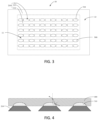
- FIG. 3 is a first top view of a display panel according to the present application.
- the display panel 10 includes a display area 11 and a non-display area 12 surrounding the display area 11.
- the pixel definition structure 210 includes a first part 212 and a second part 213.
- the first part 212 is located at the display area 11.
- the second part 213 is located at the non-display area 12.
- a water and oxygen adsorption part 310 is disposed on the first part 212.
- the water and oxygen adsorption part 310 is located at a periphery of the grooves 211.
- a surface of the water and oxygen adsorption part 310 is convex.
- a material of the water and oxygen adsorption part 310 includes one or more of polyacrylate, polyvinyl alcohol, polyoxy alkane, polyurethane, acrylate, and casein.
- a shape of the water and oxygen adsorption part 310 is hemispherical.
- the display panel 10 further includes an encapsulation layer 400.
- the encapsulation layer 400 is disposed on the water and oxygen adsorption layer 300.
- the encapsulation layer 400 covers the pixel definition structure 210, the light emitting parts 220, and the water and oxygen adsorption part 310.
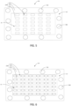
- FIG. 4 is a light path diagram of a water and oxygen adsorption layer according to the present application.
- the water and oxygen adsorption part 310 is disposed on the pixel definition structure 210, and the water and oxygen adsorption part 310 can adsorb and lock water and oxygen entering the encapsulation layer, prevent the water and oxygen from eroding the light emitting layer, and increase a lifetime of the display panel.
- a surface of the water and oxygen adsorption part 310 is configured as convex, and hence a problem that light cannot penetrate a screen to be seen by human eyes because a refractive index of a material of an encapsulation layer is less than that of air is prevented.
- the water and oxygen adsorption part is configured as convex, light emitted by the light emitting parts will reflect at the convex surface, which changes an incidence angle of the light, and therefore the light penetrates the encapsulation layer and light-emitting efficiency is increased.
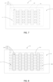
- FIG. 5 is a second top view of a display panel according to the present application.
- the water and oxygen adsorption part 310 is disposed on the second part 213.
- FIG. 6 is a third top view of a display panel according to the present application.
- the water and oxygen adsorption part 310 is disposed on the first part 212 as well as on the second part 213.
- a diameter of the water and oxygen adsorption part 310 located on the first part 212 is less than that of the water and oxygen adsorption part 310 located on the second part 213.
- the water and oxygen adsorption layer is disposed on the pixel definition structure in the display area and the non-display area, adsorbs and locks water and oxygen entering the encapsulation layer, prevents the water and oxygen from eroding the light emitting parts, and increases a lifetime of the display panel. If an incidence angle of light is excessively wide, and a refractive index of a material of an encapsulation layer is greater than that of air, the light will occur total internal reflection at an interface of the encapsulation layer such that the light cannot penetrate a screen to be seen by human eyes.
- the water and oxygen adsorption layer is configured as convex, light emitted by the light emitting parts will reflect at the convex surface, which changes an incidence angle of the light, and therefore the light penetrates the encapsulation layer and light-emitting efficiency is increased.
- FIG. 7 is a fourth top view of a display panel according to the present application.
- the water and oxygen adsorption part 310 is disposed at areas between adjacent columns and adjacent rows of grooves 211, therefore the water and oxygen adsorption part 310 does not easily fall into the grooves 211, the water and oxygen adsorption part 310 can be prepared rapidly, and production cost is further decreased.
- FIG. 8 is a fifth top view of a display panel according to the present application.
- the water and oxygen adsorption part 310 is disposed not only at gaps of columns of the grooves 211, but also at gaps of rows of the grooves 211, and thereby water and oxygen adsorption effect of the display panel is increased, and performance of the display panel is further ensured.
- the water and oxygen adsorption layer is disposed on the pixel definition structure, adsorbs and locks water and oxygen entering the encapsulation layer, prevents the water and oxygen from eroding the light emitting parts, and increases a lifetime of the display panel.
- the water and oxygen adsorption part is configured as convex, light emitted by the light emitting parts will reflect at the convex surface, which changes an incidence angle of the light, and therefore the light penetrates the encapsulation layer and light-emitting efficiency is increased.
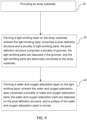
- FIG. 9 is a flowchart of a manufacturing method of a display panel according to the present application.
- the present application further provides a manufacturing method of a display panel 10 that includes: 20, providing an array substrate 100.
- a material of the flexible substrate 110 is polyimide.
- the thin film transistor layer 120 includes a gate 121, a first protection layer 122, a gate insulating layer 123, an active layer 124, a source 125, a drain 126, and a second protection layer 127.
- the first protection layer 122 covers the gate 121.
- the gate 121 is disposed on the flexible substrate 110.
- a material of the gate 121 includes one or more of Mo, Al, Ti, In, and Ga.
- the gate insulating layer 123 is disposed on the first protection layer 122.
- a material of the gate insulating layer 123 includes one or more of Al 2 O 3 , SiOx, and SiN x .
- the active layer 124 is disposed on the gate insulating layer 123.
- a material of the active layer 124 includes amorphous silicon.
- the source 125 is disposed at one end of the gate insulating layer 123 and at one end of the active layer 124.
- the drain 126 is disposed at the other end of the gate insulating layer 123 and at the other end of the active layer 124.
- the source 125 is insulated from the drain 126.
- the second protection layer 127 covers the source 125, the drain 126, and the active layer 124.
- the second protection layer 127 is configured to protect a structure of the thin film transistor layer 120 to prevent other structures or water and oxygen from affecting structures of the thin film transistor layer 120.
- the thin film transistor layer 120 further includes other structures in addition to the structures shown in FIG. 2 , and description of those structures of the thin film transistor layer 120 is omitted here.
- etching the array substrate 100 to form a placement trough 130 In another embodiment, etching the array substrate 100 to form a placement trough 130.
- the light emitting layer 200 includes a pixel definition structure 210 and a plurality of light emitting parts 220, the pixel definition structure 210 includes a plurality of grooves 211, the light emitting parts 220 are disposed in the grooves 211, and the light emitting parts 220 are electrically connected to the array substrate 100.
- the light emitting layer 200 includes the pixel definition structure 210, the plurality of light emitting parts 220, and a cathode 230.
- the cathode 230 is disposed in the placement trough 130 and on the array substrate 100.
- the pixel definition structure 210 is disposed on the array substrate 100 and on the cathode 230.
- the pixel definition structure 210 includes a plurality of grooves 211.
- the display panel 10 includes a display area 11 and a non-display area 12 surrounding the display area 11.
- the pixel definition structure 210 includes a first part 212 and a second part 213. The first part 212 is located at the display area 11.
- the second part 213 is located at the non-display area 12.
- the light emitting parts 220 are disposed in the grooves 211 and at the display area 11.
- the light emitting parts 220 are electrically connected to the array substrate 100.
- a water and oxygen adsorption layer 300 on the light emitting layer 200, wherein the water and oxygen adsorption layer 300 includes a plurality of water and oxygen adsorption parts 310, the water and oxygen adsorption parts 310 are disposed on the pixel definition structure 210, and a surface of the water and oxygen adsorption parts 310 is convex.
- a material of the water and oxygen adsorption layer 300 is printed on the light emitting layer 200, and is cured using ultraviolet light to form the water and oxygen adsorption layer 300.
- the water and oxygen adsorption layer 300 includes a plurality of water and oxygen adsorption parts 310.
- An upper surface of the water and oxygen adsorption parts 310 is convex.
- a structure of the water and oxygen adsorption parts 310 is a hemispherical structure.
- a material of the water and oxygen adsorption layer 300 includes one or more of polyacrylate, polyvinyl alcohol, polyoxy alkane, polyurethane, acrylate, and casein.
- the water and oxygen adsorption parts 310 are disposed on the second part 213.
- the water and oxygen adsorption parts 310 are disposed on the first part 212.
- the water and oxygen adsorption parts 310 are disposed on the first part 212 as well as on the second part 213.
- a diameter of the water and oxygen adsorption parts 310 located on the first part 212 is less than that of the water and oxygen adsorption parts 310 located on the second part 213.
- the water and oxygen adsorption parts 310 are disposed at areas between adjacent columns and adjacent rows of grooves 211.
- the water and oxygen adsorption parts are disposed at the areas between adjacent columns and adjacent rows of grooves, because the areas between adjacent columns and adjacent rows of grooves are large, the water and oxygen adsorption parts do not easily fall into the grooves during the manufacturing processes, the water and oxygen adsorption parts can be prepared rapidly, production cycle is shortened, and production cost is decreased.
- the water and oxygen adsorption parts 310 are disposed not only at gaps of columns of the grooves 211, but also at gaps of rows of the grooves 211.
- the encapsulation layer 400 covers the pixel definition structure 210, the light emitting parts 220, and the water and oxygen adsorption parts 310.
- the present application provides a display panel and a manufacturing method thereof.
- a water and oxygen adsorption layer is disposed on a pixel definition structure, wherein the water and oxygen adsorption layer includes a plurality of water and oxygen adsorption parts that adsorb and lock water and oxygen entering an encapsulation layer, prevent the water and oxygen from eroding light emitting parts, and increase a lifetime of the display panel.
- the water and oxygen adsorption parts are configured as convex, and light emitted by the light emitting parts will reflect at the convex surface, which changes an incidence angle of the light, and therefore the light penetrates the encapsulation layer and light-emitting efficiency is increased.
Landscapes
- Engineering & Computer Science (AREA)
- Microelectronics & Electronic Packaging (AREA)
- Physics & Mathematics (AREA)
- Optics & Photonics (AREA)
- Manufacturing & Machinery (AREA)
- Electroluminescent Light Sources (AREA)
Applications Claiming Priority (2)
| Application Number | Priority Date | Filing Date | Title |
|---|---|---|---|
| CN202010222095.7A CN111403623A (zh) | 2020-03-26 | 2020-03-26 | 一种显示面板及其制备方法 |
| PCT/CN2020/084258 WO2021189555A1 (zh) | 2020-03-26 | 2020-04-10 | 一种显示面板及其制备方法 |
Publications (2)
| Publication Number | Publication Date |
|---|---|
| EP4131449A1 true EP4131449A1 (de) | 2023-02-08 |
| EP4131449A4 EP4131449A4 (de) | 2024-05-01 |
Family
ID=71414048
Family Applications (1)
| Application Number | Title | Priority Date | Filing Date |
|---|---|---|---|
| EP20750161.0A Pending EP4131449A4 (de) | 2020-03-26 | 2020-04-10 | Anzeigetafel und herstellungsverfahren dafür |
Country Status (4)
| Country | Link |
|---|---|
| US (1) | US11937489B2 (de) |
| EP (1) | EP4131449A4 (de) |
| CN (1) | CN111403623A (de) |
| WO (1) | WO2021189555A1 (de) |
Families Citing this family (2)
| Publication number | Priority date | Publication date | Assignee | Title |
|---|---|---|---|---|
| CN114335101B (zh) * | 2021-12-28 | 2024-11-22 | 深圳市华星光电半导体显示技术有限公司 | 显示面板及其制备方法 |
| CN116075173B (zh) * | 2023-01-19 | 2025-07-15 | 北京京东方技术开发有限公司 | 一种显示面板及显示装置 |
Family Cites Families (16)
| Publication number | Priority date | Publication date | Assignee | Title |
|---|---|---|---|---|
| CN1195391C (zh) * | 2002-06-14 | 2005-03-30 | 光磊科技股份有限公司 | 有机电激发光元件 |
| JP2008300169A (ja) * | 2007-05-31 | 2008-12-11 | Seiko Epson Corp | 有機el装置、電子機器、および有機el装置の製造方法 |
| TWI607670B (zh) * | 2009-01-08 | 2017-12-01 | 半導體能源研究所股份有限公司 | 發光裝置及電子裝置 |
| KR101801913B1 (ko) * | 2012-03-23 | 2017-11-28 | 삼성디스플레이 주식회사 | 유기 발광 디스플레이 장치와, 이의 제조 방법 |
| KR101982073B1 (ko) | 2012-10-12 | 2019-05-27 | 삼성디스플레이 주식회사 | 유기 발광 소자 및 유기 발광 표시 장치 |
| KR101431338B1 (ko) * | 2012-11-26 | 2014-08-19 | 삼성디스플레이 주식회사 | 유기발광 표시장치 및 그의 제조방법 |
| KR101402606B1 (ko) * | 2012-12-07 | 2014-06-03 | 전자부품연구원 | 능동 매트릭스 디스플레이의 화소 구조 및 제조 방법 |
| KR102064392B1 (ko) * | 2013-06-04 | 2020-01-10 | 삼성디스플레이 주식회사 | 유기발광표시장치 및 그 제조방법 |
| JP6275439B2 (ja) * | 2013-09-30 | 2018-02-07 | 株式会社ジャパンディスプレイ | エレクトロルミネセンス装置およびその製造方法 |
| JP2015201354A (ja) * | 2014-04-08 | 2015-11-12 | 株式会社ジャパンディスプレイ | 有機el表示装置 |
| CN103972267B (zh) * | 2014-04-16 | 2016-09-14 | 京东方科技集团股份有限公司 | 一种有机发光显示装置 |
| TWI549330B (zh) * | 2014-06-04 | 2016-09-11 | 群創光電股份有限公司 | 有機發光二極體顯示器 |
| CN104979375A (zh) | 2015-05-28 | 2015-10-14 | 京东方科技集团股份有限公司 | 一种显示基板及其制作方法、显示装置 |
| CN105826357A (zh) * | 2016-05-16 | 2016-08-03 | 京东方科技集团股份有限公司 | 一种显示基板及oled显示装置 |
| CN109427846B (zh) * | 2017-08-28 | 2021-07-27 | 上海和辉光电股份有限公司 | 一种阵列基板及其制作方法、显示面板、显示装置 |
| CN109638059A (zh) * | 2018-12-20 | 2019-04-16 | 武汉华星光电半导体显示技术有限公司 | Oled显示面板及其制备方法、显示装置 |
-
2020
- 2020-03-26 CN CN202010222095.7A patent/CN111403623A/zh active Pending
- 2020-04-10 US US16/959,108 patent/US11937489B2/en active Active
- 2020-04-10 WO PCT/CN2020/084258 patent/WO2021189555A1/zh not_active Ceased
- 2020-04-10 EP EP20750161.0A patent/EP4131449A4/de active Pending
Also Published As
| Publication number | Publication date |
|---|---|
| EP4131449A4 (de) | 2024-05-01 |
| US20230157137A1 (en) | 2023-05-18 |
| US11937489B2 (en) | 2024-03-19 |
| CN111403623A (zh) | 2020-07-10 |
| WO2021189555A1 (zh) | 2021-09-30 |
Similar Documents
| Publication | Publication Date | Title |
|---|---|---|
| CN110416434B (zh) | 显示基板及其制备方法、显示装置 | |
| US11871606B2 (en) | Display substrate and display device | |
| US10615370B2 (en) | Light-emitting display panel | |
| JP7203763B2 (ja) | 表示基板及びその製造方法、表示装置 | |
| US10033017B2 (en) | Organic light emitting display device and method of manufacturing the same | |
| US8969904B2 (en) | Organic light emitting display device | |
| US11024687B2 (en) | Array substrate with a pixel defining layer with groove between sub-pixel areas | |
| US11245094B2 (en) | Display substrate and manufacture method thereof, display panel | |
| WO2021185045A1 (zh) | 阵列基板及其制备方法、显示装置 | |
| US9595691B2 (en) | Organic light emitting diode device | |
| TW202114210A (zh) | 可拉伸顯示面板 | |
| US20080238303A1 (en) | Organic light emitting display device having desicant layer and method of manufacturing the same | |
| WO2020211288A1 (zh) | 显示面板及显示装置 | |
| CN109166882A (zh) | 显示面板及其形成方法、显示装置 | |
| US20090179550A1 (en) | Organic light emitting display device having protecting layers and method of manufacturing the same | |
| US20210408461A1 (en) | Organic light emitting diode display panel and manufacturing method thereof | |
| CN111312798A (zh) | 柔性显示面板及其制作方法 | |
| US11937489B2 (en) | Water absorption layer mounted on light emitting layer for array substrate | |
| CN110581229B (zh) | 显示面板、显示装置及显示面板的制备方法 | |
| CN109461760B (zh) | 有机发光显示面板与显示装置 | |
| CN212085044U (zh) | 一种显示装置 | |
| US10944074B2 (en) | Organic electroluminescent display device and method for producing same | |
| US11355560B2 (en) | Touch display panel including touch unit disposed between pixel defining layers and/or between pixel defining layer and encapsulation layer | |
| KR102293507B1 (ko) | 유기 발광 표시 장치 및 이를 제조하기 위한 박막 증착용 마스크 | |
| US20230363202A1 (en) | Display substrate, display panel and display device |
Legal Events
| Date | Code | Title | Description |
|---|---|---|---|
| STAA | Information on the status of an ep patent application or granted ep patent |
Free format text: STATUS: UNKNOWN |
|
| STAA | Information on the status of an ep patent application or granted ep patent |
Free format text: STATUS: THE INTERNATIONAL PUBLICATION HAS BEEN MADE |
|
| PUAI | Public reference made under article 153(3) epc to a published international application that has entered the european phase |
Free format text: ORIGINAL CODE: 0009012 |
|
| STAA | Information on the status of an ep patent application or granted ep patent |
Free format text: STATUS: REQUEST FOR EXAMINATION WAS MADE |
|
| 17P | Request for examination filed |
Effective date: 20200811 |
|
| AK | Designated contracting states |
Kind code of ref document: A1 Designated state(s): AL AT BE BG CH CY CZ DE DK EE ES FI FR GB GR HR HU IE IS IT LI LT LU LV MC MK MT NL NO PL PT RO RS SE SI SK SM TR |
|
| DAV | Request for validation of the european patent (deleted) | ||
| DAX | Request for extension of the european patent (deleted) | ||
| REG | Reference to a national code |
Ref country code: DE Ref legal event code: R079 Free format text: PREVIOUS MAIN CLASS: H01L0051520000 Ipc: H10K0059800000 |
|
| A4 | Supplementary search report drawn up and despatched |
Effective date: 20240405 |
|
| RIC1 | Information provided on ipc code assigned before grant |
Ipc: H10K 59/122 20230101ALI20240328BHEP Ipc: H10K 59/80 20230101AFI20240328BHEP |