EP4131451A1 - Structure d'encapsulation d'oled et procédé d'encapsulation d'oled, et appareil d'affichage oled - Google Patents
Structure d'encapsulation d'oled et procédé d'encapsulation d'oled, et appareil d'affichage oled Download PDFInfo
- Publication number
- EP4131451A1 EP4131451A1 EP20754609.4A EP20754609A EP4131451A1 EP 4131451 A1 EP4131451 A1 EP 4131451A1 EP 20754609 A EP20754609 A EP 20754609A EP 4131451 A1 EP4131451 A1 EP 4131451A1
- Authority
- EP
- European Patent Office
- Prior art keywords
- oled
- encapsulation layer
- self
- healing
- layers
- Prior art date
- Legal status (The legal status is an assumption and is not a legal conclusion. Google has not performed a legal analysis and makes no representation as to the accuracy of the status listed.)
- Pending
Links
- 238000000034 method Methods 0.000 title claims abstract description 16
- 238000004806 packaging method and process Methods 0.000 title 2
- 238000005538 encapsulation Methods 0.000 claims abstract description 183
- 239000000758 substrate Substances 0.000 claims abstract description 32
- 239000000463 material Substances 0.000 claims description 31
- CQEYYJKEWSMYFG-UHFFFAOYSA-N butyl acrylate Chemical compound CCCCOC(=O)C=C CQEYYJKEWSMYFG-UHFFFAOYSA-N 0.000 claims description 19
- VVQNEPGJFQJSBK-UHFFFAOYSA-N Methyl methacrylate Chemical compound COC(=O)C(C)=C VVQNEPGJFQJSBK-UHFFFAOYSA-N 0.000 claims description 17
- 239000003795 chemical substances by application Substances 0.000 claims description 7
- 239000000203 mixture Substances 0.000 claims description 4
- 229910052581 Si3N4 Inorganic materials 0.000 claims description 3
- 230000015572 biosynthetic process Effects 0.000 claims description 3
- 238000005755 formation reaction Methods 0.000 claims description 3
- HQVNEWCFYHHQES-UHFFFAOYSA-N silicon nitride Chemical compound N12[Si]34N5[Si]62N3[Si]51N64 HQVNEWCFYHHQES-UHFFFAOYSA-N 0.000 claims description 3
- 238000007872 degassing Methods 0.000 claims description 2
- 238000005507 spraying Methods 0.000 claims description 2
- QVGXLLKOCUKJST-UHFFFAOYSA-N atomic oxygen Chemical compound [O] QVGXLLKOCUKJST-UHFFFAOYSA-N 0.000 abstract description 8
- 229910052760 oxygen Inorganic materials 0.000 abstract description 8
- 239000001301 oxygen Substances 0.000 abstract description 8
- XLYOFNOQVPJJNP-UHFFFAOYSA-N water Substances O XLYOFNOQVPJJNP-UHFFFAOYSA-N 0.000 abstract description 8
- 230000032683 aging Effects 0.000 description 6
- BAPJBEWLBFYGME-UHFFFAOYSA-N Methyl acrylate Chemical compound COC(=O)C=C BAPJBEWLBFYGME-UHFFFAOYSA-N 0.000 description 4
- 239000004642 Polyimide Substances 0.000 description 4
- 229920001721 polyimide Polymers 0.000 description 4
- 230000003647 oxidation Effects 0.000 description 3
- 238000007254 oxidation reaction Methods 0.000 description 3
- 238000005516 engineering process Methods 0.000 description 2
- 239000011521 glass Substances 0.000 description 2
- -1 polyethylene terephthalate Polymers 0.000 description 2
- 239000004695 Polyether sulfone Substances 0.000 description 1
- 229910004205 SiNX Inorganic materials 0.000 description 1
- 230000005540 biological transmission Effects 0.000 description 1
- 230000000903 blocking effect Effects 0.000 description 1
- 230000015556 catabolic process Effects 0.000 description 1
- 238000005229 chemical vapour deposition Methods 0.000 description 1
- 238000006731 degradation reaction Methods 0.000 description 1
- 230000018109 developmental process Effects 0.000 description 1
- 238000010586 diagram Methods 0.000 description 1
- 230000014509 gene expression Effects 0.000 description 1
- 230000035876 healing Effects 0.000 description 1
- 230000005525 hole transport Effects 0.000 description 1
- 239000002184 metal Substances 0.000 description 1
- 238000012986 modification Methods 0.000 description 1
- 230000004048 modification Effects 0.000 description 1
- 229920003207 poly(ethylene-2,6-naphthalate) Polymers 0.000 description 1
- 229920000515 polycarbonate Polymers 0.000 description 1
- 239000004417 polycarbonate Substances 0.000 description 1
- 229920006393 polyether sulfone Polymers 0.000 description 1
- 239000011112 polyethylene naphthalate Substances 0.000 description 1
- 229920000139 polyethylene terephthalate Polymers 0.000 description 1
- 239000005020 polyethylene terephthalate Substances 0.000 description 1
- 230000008569 process Effects 0.000 description 1
- 230000004044 response Effects 0.000 description 1
- 239000010409 thin film Substances 0.000 description 1
Images
Classifications
-
- H—ELECTRICITY
- H10—SEMICONDUCTOR DEVICES; ELECTRIC SOLID-STATE DEVICES NOT OTHERWISE PROVIDED FOR
- H10K—ORGANIC ELECTRIC SOLID-STATE DEVICES
- H10K59/00—Integrated devices, or assemblies of multiple devices, comprising at least one organic light-emitting element covered by group H10K50/00
- H10K59/80—Constructional details
- H10K59/87—Passivation; Containers; Encapsulations
- H10K59/873—Encapsulations
- H10K59/8731—Encapsulations multilayered coatings having a repetitive structure, e.g. having multiple organic-inorganic bilayers
-
- H—ELECTRICITY
- H10—SEMICONDUCTOR DEVICES; ELECTRIC SOLID-STATE DEVICES NOT OTHERWISE PROVIDED FOR
- H10K—ORGANIC ELECTRIC SOLID-STATE DEVICES
- H10K50/00—Organic light-emitting devices
- H10K50/80—Constructional details
- H10K50/84—Passivation; Containers; Encapsulations
- H10K50/844—Encapsulations
-
- H—ELECTRICITY
- H10—SEMICONDUCTOR DEVICES; ELECTRIC SOLID-STATE DEVICES NOT OTHERWISE PROVIDED FOR
- H10K—ORGANIC ELECTRIC SOLID-STATE DEVICES
- H10K71/00—Manufacture or treatment specially adapted for the organic devices covered by this subclass
Definitions
- the present application relates to a technical field of display panel encapsulation, and in particular, to an organic light-emitting diode (OLED) encapsulation structure, a method of encapsulating an organic light-emitting diode (OLED), and an organic light-emitting diode (OLED) display device.
- OLED organic light-emitting diode
- OLED organic light-emitting diode
- the main component of an organic light-emitting diode (OLED) display device is an OLED display panel, which includes a glass substrate, a polyimide, polyimide (PI) flexible layer, a thin film transistor (TFT) driving layer, an OLED light-emitting layer, a first inorganic encapsulation layer, an organic encapsulation layer, and a second inorganic encapsulation layer, wherein the organic encapsulation layer mainly plays a role of planarization and blocking water and oxygen transmission.
- the inventors found that the conventional technology has at least the problem that cracks are prone to occur in the organic encapsulation layer in the conventional OLED display panel, so that water and oxygen can enter the interior of the OLED display panel through the cracks to accelerate the aging of the OLED device.
- an organic light-emitting diode (OLED) encapsulation structure a method of encapsulating an organic light-emitting diode (OLED), and an organic light-emitting diode (OLED) display device, to solve the problem that cracks are prone to occur in the organic encapsulation layer in the conventional OLED display panel, so that water and oxygen can enter the interior of the OLED display panel through the cracks to accelerate the aging of the OLED device.
- an embodiment of the present application provides an organic light-emitting diode (OLED) encapsulation structure including a substrate, a self-healing encapsulation layer, and at least two inorganic encapsulation layers,
- OLED organic light-emitting diode
- an embodiment of the present application further provides a method of encapsulating an organic light-emitting diode (OLED), including the following steps:
- an embodiment of the present application further provides an organic light-emitting diode (OLED) display device including an OLED display panel which includes an OLED encapsulation structure, wherein
- OLED organic light-emitting diode
- the OLED encapsulation structure includes: a substrate, a self-healing encapsulation layer, and at least two inorganic encapsulation layers, wherein an OLED device is fabricated on the substrate, a cavity is formed between two adjacent layers of the inorganic encapsulation layers, a layer of the self-healing encapsulation layer is provided in the cavity, and one of the inorganic encapsulation layers covers the OLED device; and wherein a number of layers of the self-healing encapsulation layer is one less than a number of layers of the inorganic encapsulation layers, and the self-healing encapsulation layer is made of a material including methyl methacrylate and n-butyl acrylate that are mixed in a preset molar ratio.
- the self-healing encapsulation layer is used to achieve self-healing of cracks at room temperature to prevent water and oxygen from entering the interior of the OLED panel through cracks to accelerate the aging of the OLED device, and as a result, the oxidation resistance of the OLED display panel is improved.
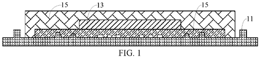
- an organic light-emitting diode (OLED) encapsulation structure includes a substrate 11, a self-healing encapsulation layer 13, and at least two inorganic encapsulation layers 15.
- a number of layers of the self-healing encapsulation layer 13 is one less than a number of layers of the inorganic encapsulation layers, 15 and the self-healing encapsulation layer 13 is made of a material including methyl methacrylate and n-butyl acrylate that are mixed in a preset molar ratio.
- An OLED device is fabricated on the substrate 11, a cavity is formed between two adjacent layers of the inorganic encapsulation layers 15, a layer of the self-healing encapsulation layer 13 is provided in the cavity, and one of the inorganic encapsulation layers 15 covers the OLED device.
- the substrate 11 is a carrier substrate for the OLED device and the organic light-emitting diode (OLED) encapsulation structure, and it is transparent.
- the substrate 11 may made of, but is not limited to, the following materials: polyimide, polyethylene terephthalate, polyethylene naphthalate, polycarbonate, polyethersulfone, and/or glass.
- OLED devices are fabricated on the substrate 11.
- the OLED devices include an anode, a hole transport layer, an OLED light-emitting layer, an electron transport layer, and a metal cathode, which are sequentially disposed in a direction away from the substrate 11.
- a combination of a self-healing encapsulation layer 13 and at least two inorganic encapsulation layers 15 is used.
- the self-healing encapsulation layer 13 is capable of healing cracks at room temperature by itself, and made of a material including methyl methacrylate and n-butyl acrylate that are mixed in a preset molar ratio. Specifically, the preset molar ratio ranges from 45/55 to 55/45. In one example, the molar ratio of methyl acrylate and n-butyl acrylate is 50/50. In another example, the molar ratio of methyl acrylate and n-butyl acrylate is 40/50.
- the material of the self-healing encapsulation layer 13 further includes a curing agent.
- the inorganic encapsulation layers 15 are used to provide physical protection for the OLED device.
- the inorganic encapsulation layers 15 may be made of, but is not limited to, silicon nitride (SiNx).
- a number of layers of the inorganic encapsulation layers 15 is one more than a number of layers of the self-healing encapsulation layer 13. After the encapsulation is completed, one self-healing encapsulation layer 13 is sandwiched between every two inorganic encapsulation layers 15.
- an organic light-emitting diode (OLED) encapsulation structure includes a substrate 11, a self-healing encapsulation layer 13, and two inorganic encapsulation layers 15.
- the self-healing encapsulation layer 13 is made of a material including methyl methacrylate and n-butyl acrylate that are mixed in a preset molar ratio.
- An OLED device is fabricated on the substrate 11, one self-healing encapsulation layer 13 is sandwiched between two inorganic encapsulation layers 15, and one of the inorganic encapsulation layers 15 covers the OLED device.
- the OLED encapsulation structure includes a substrate 11, a self-healing encapsulation layer 13, and at least two inorganic encapsulation layers 15; an OLED device is fabricated on the substrate 11; one of the self-healing encapsulation layer 13 is sandwiched between adjacent layers of the inorganic encapsulation layers 15, and one of the inorganic encapsulation layers 15 covers the OLED device.
- a number of layers of the self-healing encapsulation layer 13 is one less than a number of layers of the inorganic encapsulation layers 15, and the self-healing encapsulation layer is made of a material including methyl methacrylate and n-butyl acrylate that are mixed in a preset molar ratio.
- the self-healing encapsulation layer 13 is used to achieve self-healing of cracks at room temperature to prevent water and oxygen from entering the interior of the OLED panel through cracks to accelerate the aging of the OLED device, and as a result, the oxidation resistance of the OLED display panel is improved.
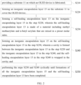
- a method of encapsulating an organic light-emitting diode including the following steps:
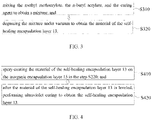
- the material of the self-healing encapsulation layer 13 includes methyl methacrylate, n-butyl acrylate, and a curing agent. As shown in FIG. 3 , the material of the self-healing encapsulation layer 13 is prepared based on the following specific steps:
- the inorganic encapsulation layer 15 can be made by, but not limited to, chemical vapor deposition.
- the step of forming a self-healing encapsulation layer on the inorganic encapsulation layer in the step S220 includes the steps as follows:
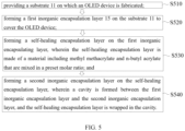
- the method of encapsulating the OLED includes the following steps:
- steps in the flowchart of FIG. 2-5 are sequentially displayed according to the directions of the arrows, these steps are not necessarily performed sequentially in the order indicated by the arrows. Unless explicitly stated in this document, the execution of these steps is not strictly limited, and these steps can be performed in other orders. Moreover, at least a part of the steps in FIG. 2-5 may include multiple sub-steps or stages, and these sub-steps or stages are not necessarily performed at the same time, but may be performed at different times. In addition, the execution order of these sub-steps or stages is not necessarily performed sequentially, but may be performed in turn or alternately with other steps or at least a part of sub-steps or stages of other steps.
- an organic light-emitting diode (OLED) display device which includes an OLED display panel that contains the above-mentioned OLED encapsulation structure.
- the OLED encapsulation structure in this embodiment is the same as the OLED encapsulation structure described in each of embodiments for illustrating the OLED encapsulation structure of the present application.
- the OLED display device is provided with a self-healing encapsulation layer 13 that heals the cracks on its own, slowing down the degradation of the OLED device and extending the service life of the OLED display device.
Landscapes
- Chemical & Material Sciences (AREA)
- Inorganic Chemistry (AREA)
- Physics & Mathematics (AREA)
- Optics & Photonics (AREA)
- Engineering & Computer Science (AREA)
- Manufacturing & Machinery (AREA)
- Electroluminescent Light Sources (AREA)
Applications Claiming Priority (2)
| Application Number | Priority Date | Filing Date | Title |
|---|---|---|---|
| CN202010224021.7A CN111403626B (zh) | 2020-03-26 | 2020-03-26 | Oled封装结构、oled封装方法和oled显示装置 |
| PCT/CN2020/084043 WO2021189539A1 (fr) | 2020-03-26 | 2020-04-09 | Structure d'encapsulation d'oled et procédé d'encapsulation d'oled, et appareil d'affichage oled |
Publications (2)
| Publication Number | Publication Date |
|---|---|
| EP4131451A1 true EP4131451A1 (fr) | 2023-02-08 |
| EP4131451A4 EP4131451A4 (fr) | 2024-05-15 |
Family
ID=71431252
Family Applications (1)
| Application Number | Title | Priority Date | Filing Date |
|---|---|---|---|
| EP20754609.4A Pending EP4131451A4 (fr) | 2020-03-26 | 2020-04-09 | Structure d'encapsulation d'oled et procédé d'encapsulation d'oled, et appareil d'affichage oled |
Country Status (4)
| Country | Link |
|---|---|
| US (1) | US11380870B2 (fr) |
| EP (1) | EP4131451A4 (fr) |
| CN (1) | CN111403626B (fr) |
| WO (1) | WO2021189539A1 (fr) |
Families Citing this family (3)
| Publication number | Priority date | Publication date | Assignee | Title |
|---|---|---|---|---|
| CN112280505B (zh) * | 2020-10-27 | 2022-04-26 | 武汉华星光电半导体显示技术有限公司 | Uv胶及其制备方法、显示装置 |
| US20240180017A1 (en) * | 2021-03-29 | 2024-05-30 | Sharp Kabushiki Kaisha | Display device and method for producing display device |
| CN117479784B (zh) * | 2023-12-06 | 2024-07-09 | 惠科股份有限公司 | 显示面板及显示装置 |
Family Cites Families (15)
| Publication number | Priority date | Publication date | Assignee | Title |
|---|---|---|---|---|
| JP5133228B2 (ja) | 2008-12-04 | 2013-01-30 | 株式会社ジャパンディスプレイイースト | 有機el表示装置の製造方法および有機el表示装置 |
| KR101424395B1 (ko) * | 2012-05-31 | 2014-07-28 | 주식회사 엘지화학 | 유기전자장치의 제조방법 |
| KR101445311B1 (ko) * | 2012-08-27 | 2014-09-30 | 엘지디스플레이 주식회사 | 필름 포토레지스트 및 이를 이용한 유기전계발광표시장치의 제조방법 |
| KR20140071552A (ko) * | 2012-11-23 | 2014-06-12 | 삼성디스플레이 주식회사 | 유기 발광 디스플레이 장치 및 그 제조 방법 |
| WO2014124072A2 (fr) * | 2013-02-07 | 2014-08-14 | University Of Massachusetts | Polyoléfine fonctionnalisée par de la coumarine et produits de cyclodimérisation associés, procédés de préparation et dispositifs électroniques |
| JP6167459B2 (ja) * | 2013-11-01 | 2017-07-26 | パナソニックIpマネジメント株式会社 | 有機エレクトロルミネッセンスデバイス |
| KR20180015223A (ko) | 2015-06-03 | 2018-02-12 | 쓰리엠 이노베이티브 프로퍼티즈 컴파니 | 가요성 디스플레이를 위한 아크릴 블록 공중합체-기반 조립체 층 |
| CN106409873B (zh) * | 2016-10-12 | 2019-06-04 | 上海天马微电子有限公司 | 柔性显示装置及制造方法 |
| JP7105543B2 (ja) * | 2017-05-26 | 2022-07-25 | エルジー ディスプレイ カンパニー リミテッド | 有機表示素子 |
| CN107369781B (zh) | 2017-08-29 | 2024-02-27 | 京东方科技集团股份有限公司 | 封装结构和有机发光显示装置 |
| US10920061B2 (en) * | 2017-12-29 | 2021-02-16 | Kyungpook National University Industry-Academic Cooperation Foundation | Self-healing acrylic copolymer, crosslinked copolymer prepared from the acrylic copolymer and method for low-temperature self-healing of the crosslinked copolymer |
| CN109503035B (zh) * | 2018-12-14 | 2021-06-08 | 江南大学 | 一种含粘土超亲水防雾可自愈复合薄膜的制备方法 |
| US11081422B2 (en) * | 2019-03-14 | 2021-08-03 | Toyota Motor Engineering & Manufacturing North America, Inc. | Self-healing PDMS encapsulation and repair of power modules |
| CN110048016B (zh) * | 2019-03-26 | 2020-09-08 | 武汉华星光电半导体显示技术有限公司 | 薄膜封装结构、oled显示面板及其制作方法 |
| CN110452399B (zh) * | 2019-07-22 | 2020-12-11 | 中国科学院过程工程研究所 | 一种可室温自修复聚合物薄膜的制备方法 |
-
2020
- 2020-03-26 CN CN202010224021.7A patent/CN111403626B/zh active Active
- 2020-04-09 US US16/770,514 patent/US11380870B2/en active Active
- 2020-04-09 EP EP20754609.4A patent/EP4131451A4/fr active Pending
- 2020-04-09 WO PCT/CN2020/084043 patent/WO2021189539A1/fr not_active Ceased
Also Published As
| Publication number | Publication date |
|---|---|
| CN111403626B (zh) | 2021-07-06 |
| US20220037618A1 (en) | 2022-02-03 |
| CN111403626A (zh) | 2020-07-10 |
| US11380870B2 (en) | 2022-07-05 |
| WO2021189539A1 (fr) | 2021-09-30 |
| EP4131451A4 (fr) | 2024-05-15 |
Similar Documents
| Publication | Publication Date | Title |
|---|---|---|
| EP4131451A1 (fr) | Structure d'encapsulation d'oled et procédé d'encapsulation d'oled, et appareil d'affichage oled | |
| US10998522B2 (en) | Flexible OLED display panel, manufacturing method for the same and display device | |
| US11737316B2 (en) | Display panels and manufacturing methods thereof | |
| US10818876B2 (en) | Organic light-emitting diode (OLED) display panel and manufacturing method thereof | |
| CN1967858B (zh) | 电发光显示器和电子设备 | |
| US10658611B2 (en) | Encapsulation method of OLED panel and a encapsulation structure thereof | |
| EP3270434B1 (fr) | Panneau d'affichage électroluminescent organique à émission par le haut, son procédé de fabrication et dispositif d'affichage | |
| US11362290B2 (en) | Display substrate, method of manufacturing display substrate, and display apparatus | |
| CN108598286B (zh) | 一种oled显示面板以及封装方法 | |
| CN108807494B (zh) | 显示基板及其制作方法、显示面板和显示装置 | |
| US20210376288A1 (en) | Display panel and display device | |
| US11139453B2 (en) | Flexible display panel having blocking walls | |
| US20170062757A1 (en) | Flexible oled display and method for manufacturing the same | |
| US11075360B2 (en) | Display panel, display device and method for manufacturing display panel | |
| US20200028115A1 (en) | Method of encapsulating a flexible oled panel and encapsulation structure | |
| US20210384463A1 (en) | Display panel, manufacturing method thereof and display module | |
| US20190206963A1 (en) | Display panel and method for manufacturing the same | |
| US20150171150A1 (en) | Manufacturing method of organic light emitting diode display device | |
| CN113471380A (zh) | 一种显示装置及其封装方法 | |
| US11502262B2 (en) | Packaging structure of electroluminescent element, method for manufacturing the same, display device | |
| US20160365538A1 (en) | Packaging structure of oled device and packaging method thereof | |
| US11342531B2 (en) | Organic light emitting diode display panel having a touch function layer | |
| WO2024260038A1 (fr) | Écran d'affichage et appareil d'affichage | |
| US20190229280A1 (en) | Flexible oled display and manufacturing method thereof | |
| US10263055B2 (en) | Pixel definition structure, organic light-emitting device, encapsulation method thereof, and display apparatus |
Legal Events
| Date | Code | Title | Description |
|---|---|---|---|
| STAA | Information on the status of an ep patent application or granted ep patent |
Free format text: STATUS: UNKNOWN |
|
| STAA | Information on the status of an ep patent application or granted ep patent |
Free format text: STATUS: THE INTERNATIONAL PUBLICATION HAS BEEN MADE |
|
| PUAI | Public reference made under article 153(3) epc to a published international application that has entered the european phase |
Free format text: ORIGINAL CODE: 0009012 |
|
| STAA | Information on the status of an ep patent application or granted ep patent |
Free format text: STATUS: REQUEST FOR EXAMINATION WAS MADE |
|
| 17P | Request for examination filed |
Effective date: 20200821 |
|
| AK | Designated contracting states |
Kind code of ref document: A1 Designated state(s): AL AT BE BG CH CY CZ DE DK EE ES FI FR GB GR HR HU IE IS IT LI LT LU LV MC MK MT NL NO PL PT RO RS SE SI SK SM TR |
|
| DAV | Request for validation of the european patent (deleted) | ||
| DAX | Request for extension of the european patent (deleted) | ||
| REG | Reference to a national code |
Ref country code: DE Ref legal event code: R079 Free format text: PREVIOUS MAIN CLASS: H01L0051520000 Ipc: H10K0050844000 |
|
| A4 | Supplementary search report drawn up and despatched |
Effective date: 20240416 |
|
| RIC1 | Information provided on ipc code assigned before grant |
Ipc: H10K 71/00 20230101ALI20240410BHEP Ipc: C08J 5/18 20060101ALI20240410BHEP Ipc: H10K 50/844 20230101AFI20240410BHEP |