EP4131677B1 - Laser à cristal photonique bidimensionnel - Google Patents
Laser à cristal photonique bidimensionnel Download PDFInfo
- Publication number
- EP4131677B1 EP4131677B1 EP21781958.0A EP21781958A EP4131677B1 EP 4131677 B1 EP4131677 B1 EP 4131677B1 EP 21781958 A EP21781958 A EP 21781958A EP 4131677 B1 EP4131677 B1 EP 4131677B1
- Authority
- EP
- European Patent Office
- Prior art keywords
- layer
- dimensional photonic
- type semiconductor
- crystal
- electrode
- Prior art date
- Legal status (The legal status is an assumption and is not a legal conclusion. Google has not performed a legal analysis and makes no representation as to the accuracy of the status listed.)
- Active
Links
Images


Classifications
-
- H—ELECTRICITY
- H01—ELECTRIC ELEMENTS
- H01S—DEVICES USING THE PROCESS OF LIGHT AMPLIFICATION BY STIMULATED EMISSION OF RADIATION [LASER] TO AMPLIFY OR GENERATE LIGHT; DEVICES USING STIMULATED EMISSION OF ELECTROMAGNETIC RADIATION IN WAVE RANGES OTHER THAN OPTICAL
- H01S5/00—Semiconductor lasers
- H01S5/10—Construction or shape of the optical resonator, e.g. extended or external cavity, coupled cavities, bent-guide, varying width, thickness or composition of the active region
- H01S5/11—Comprising a photonic bandgap structure
-
- H—ELECTRICITY
- H01—ELECTRIC ELEMENTS
- H01S—DEVICES USING THE PROCESS OF LIGHT AMPLIFICATION BY STIMULATED EMISSION OF RADIATION [LASER] TO AMPLIFY OR GENERATE LIGHT; DEVICES USING STIMULATED EMISSION OF ELECTROMAGNETIC RADIATION IN WAVE RANGES OTHER THAN OPTICAL
- H01S5/00—Semiconductor lasers
- H01S5/04—Processes or apparatus for excitation, e.g. pumping, e.g. by electron beams
- H01S5/042—Electrical excitation ; Circuits therefor
- H01S5/0425—Electrodes, e.g. characterised by the structure
- H01S5/04256—Electrodes, e.g. characterised by the structure characterised by the configuration
-
- H—ELECTRICITY
- H01—ELECTRIC ELEMENTS
- H01S—DEVICES USING THE PROCESS OF LIGHT AMPLIFICATION BY STIMULATED EMISSION OF RADIATION [LASER] TO AMPLIFY OR GENERATE LIGHT; DEVICES USING STIMULATED EMISSION OF ELECTROMAGNETIC RADIATION IN WAVE RANGES OTHER THAN OPTICAL
- H01S5/00—Semiconductor lasers
- H01S5/10—Construction or shape of the optical resonator, e.g. extended or external cavity, coupled cavities, bent-guide, varying width, thickness or composition of the active region
- H01S5/18—Surface-emitting [SE] lasers, e.g. having both horizontal and vertical cavities
- H01S5/183—Surface-emitting [SE] lasers, e.g. having both horizontal and vertical cavities having only vertical cavities, e.g. vertical cavity surface-emitting lasers [VCSEL]
- H01S5/18305—Surface-emitting [SE] lasers, e.g. having both horizontal and vertical cavities having only vertical cavities, e.g. vertical cavity surface-emitting lasers [VCSEL] with emission through the substrate, i.e. bottom emission
-
- H—ELECTRICITY
- H01—ELECTRIC ELEMENTS
- H01S—DEVICES USING THE PROCESS OF LIGHT AMPLIFICATION BY STIMULATED EMISSION OF RADIATION [LASER] TO AMPLIFY OR GENERATE LIGHT; DEVICES USING STIMULATED EMISSION OF ELECTROMAGNETIC RADIATION IN WAVE RANGES OTHER THAN OPTICAL
- H01S5/00—Semiconductor lasers
- H01S5/10—Construction or shape of the optical resonator, e.g. extended or external cavity, coupled cavities, bent-guide, varying width, thickness or composition of the active region
- H01S5/18—Surface-emitting [SE] lasers, e.g. having both horizontal and vertical cavities
- H01S5/185—Surface-emitting [SE] lasers, e.g. having both horizontal and vertical cavities having only horizontal cavities, e.g. horizontal cavity surface-emitting lasers [HCSEL]
-
- H—ELECTRICITY
- H01—ELECTRIC ELEMENTS
- H01S—DEVICES USING THE PROCESS OF LIGHT AMPLIFICATION BY STIMULATED EMISSION OF RADIATION [LASER] TO AMPLIFY OR GENERATE LIGHT; DEVICES USING STIMULATED EMISSION OF ELECTROMAGNETIC RADIATION IN WAVE RANGES OTHER THAN OPTICAL
- H01S5/00—Semiconductor lasers
- H01S5/20—Structure or shape of the semiconductor body to guide the optical wave ; Confining structures perpendicular to the optical axis, e.g. index or gain guiding, stripe geometry, broad area lasers, gain tailoring, transverse or lateral reflectors, special cladding structures, MQW barrier reflection layers
- H01S5/2004—Confining in the direction perpendicular to the layer structure
- H01S5/2018—Optical confinement, e.g. absorbing-, reflecting- or waveguide-layers
- H01S5/2027—Reflecting region or layer, parallel to the active layer, e.g. to modify propagation of the mode in the laser or to influence transverse modes
-
- H—ELECTRICITY
- H01—ELECTRIC ELEMENTS
- H01S—DEVICES USING THE PROCESS OF LIGHT AMPLIFICATION BY STIMULATED EMISSION OF RADIATION [LASER] TO AMPLIFY OR GENERATE LIGHT; DEVICES USING STIMULATED EMISSION OF ELECTROMAGNETIC RADIATION IN WAVE RANGES OTHER THAN OPTICAL
- H01S5/00—Semiconductor lasers
- H01S5/30—Structure or shape of the active region; Materials used for the active region
- H01S5/305—Structure or shape of the active region; Materials used for the active region characterised by the doping materials used in the laser structure
- H01S5/3095—Tunnel junction
-
- H—ELECTRICITY
- H01—ELECTRIC ELEMENTS
- H01S—DEVICES USING THE PROCESS OF LIGHT AMPLIFICATION BY STIMULATED EMISSION OF RADIATION [LASER] TO AMPLIFY OR GENERATE LIGHT; DEVICES USING STIMULATED EMISSION OF ELECTROMAGNETIC RADIATION IN WAVE RANGES OTHER THAN OPTICAL
- H01S5/00—Semiconductor lasers
- H01S5/04—Processes or apparatus for excitation, e.g. pumping, e.g. by electron beams
- H01S5/042—Electrical excitation ; Circuits therefor
- H01S5/0425—Electrodes, e.g. characterised by the structure
- H01S5/04254—Electrodes, e.g. characterised by the structure characterised by the shape
-
- H—ELECTRICITY
- H01—ELECTRIC ELEMENTS
- H01S—DEVICES USING THE PROCESS OF LIGHT AMPLIFICATION BY STIMULATED EMISSION OF RADIATION [LASER] TO AMPLIFY OR GENERATE LIGHT; DEVICES USING STIMULATED EMISSION OF ELECTROMAGNETIC RADIATION IN WAVE RANGES OTHER THAN OPTICAL
- H01S5/00—Semiconductor lasers
- H01S5/04—Processes or apparatus for excitation, e.g. pumping, e.g. by electron beams
- H01S5/042—Electrical excitation ; Circuits therefor
- H01S5/0425—Electrodes, e.g. characterised by the structure
- H01S5/04256—Electrodes, e.g. characterised by the structure characterised by the configuration
- H01S5/04257—Electrodes, e.g. characterised by the structure characterised by the configuration having positive and negative electrodes on the same side of the substrate
-
- H—ELECTRICITY
- H01—ELECTRIC ELEMENTS
- H01S—DEVICES USING THE PROCESS OF LIGHT AMPLIFICATION BY STIMULATED EMISSION OF RADIATION [LASER] TO AMPLIFY OR GENERATE LIGHT; DEVICES USING STIMULATED EMISSION OF ELECTROMAGNETIC RADIATION IN WAVE RANGES OTHER THAN OPTICAL
- H01S5/00—Semiconductor lasers
- H01S5/10—Construction or shape of the optical resonator, e.g. extended or external cavity, coupled cavities, bent-guide, varying width, thickness or composition of the active region
- H01S5/18—Surface-emitting [SE] lasers, e.g. having both horizontal and vertical cavities
- H01S5/183—Surface-emitting [SE] lasers, e.g. having both horizontal and vertical cavities having only vertical cavities, e.g. vertical cavity surface-emitting lasers [VCSEL]
- H01S5/18344—Surface-emitting [SE] lasers, e.g. having both horizontal and vertical cavities having only vertical cavities, e.g. vertical cavity surface-emitting lasers [VCSEL] characterized by the mesa, e.g. dimensions or shape of the mesa
- H01S5/18347—Mesa comprising active layer
-
- H—ELECTRICITY
- H01—ELECTRIC ELEMENTS
- H01S—DEVICES USING THE PROCESS OF LIGHT AMPLIFICATION BY STIMULATED EMISSION OF RADIATION [LASER] TO AMPLIFY OR GENERATE LIGHT; DEVICES USING STIMULATED EMISSION OF ELECTROMAGNETIC RADIATION IN WAVE RANGES OTHER THAN OPTICAL
- H01S5/00—Semiconductor lasers
- H01S5/30—Structure or shape of the active region; Materials used for the active region
- H01S5/34—Structure or shape of the active region; Materials used for the active region comprising quantum well or superlattice structures, e.g. single quantum well [SQW] lasers, multiple quantum well [MQW] lasers or graded index separate confinement heterostructure [GRINSCH] lasers
- H01S5/343—Structure or shape of the active region; Materials used for the active region comprising quantum well or superlattice structures, e.g. single quantum well [SQW] lasers, multiple quantum well [MQW] lasers or graded index separate confinement heterostructure [GRINSCH] lasers in AIIIBV compounds, e.g. AlGaAs-laser, InP-based laser
- H01S5/34313—Structure or shape of the active region; Materials used for the active region comprising quantum well or superlattice structures, e.g. single quantum well [SQW] lasers, multiple quantum well [MQW] lasers or graded index separate confinement heterostructure [GRINSCH] lasers in AIIIBV compounds, e.g. AlGaAs-laser, InP-based laser with a well layer having only As as V-compound, e.g. AlGaAs, InGaAs
Definitions
- the present invention relates to a two-dimensional photonic-crystal laser in which a two-dimensional photonic crystal is used for amplifying light.
- the two-dimensional photonic-crystal laser includes an active layer and a two-dimensional photonic-crystal layer.
- the active layer generates light within a specific wavelength band when supplied with carriers (carrier holes or electrons).
- the two-dimensional photonic-crystal layer has a configuration including a plate-shaped base body in which modified refractive index areas whose refractive index differs from that of the base body are periodically arranged two-dimensionally.
- the modified refractive index areas include holes (air) formed in the base body or a member different from the material of the base body.
- the two-dimensional photonic-crystal laser generally includes layers having various functions in addition to the active layer and the two-dimensional photonic-crystal layer described above.
- the two-dimensional photonic-crystal laser described in Patent Literature 1 has a structure in which a first cladding layer, an active layer, a carrier block layer, a two-dimensional photonic-crystal layer, a second cladding layer, and a contact layer are stacked in the mentioned order on a substrate.
- the lower face of the substrate and the upper face of the contact layer are each provided with an electrode.
- Each layer other than the electrode is stacked by epitaxially growing on the substrate.
- an n-type semiconductor which is less expensive than a p-type semiconductor, is used.
- the first cladding layer a semiconductor having the same polarity as the substrate, n-type, is used, and for the carrier block layer, the base body of the two-dimensional photonic-crystal layer, the second cladding layer, and the contact layer, p-type semiconductors are used.
- carrier holes are supplied into the active layer from the upper electrode through the contact layer, the second cladding layer, and the base body of the two-dimensional photonic-crystal layer, and electrons are supplied into the active layer from the lower electrode through the substrate and the first cladding layer.
- the first cladding layer and the second cladding layer are provided in order to enhance the confinement of light between the first cladding layer and the second cladding layer, so that the light emission efficiency in the active layer and the light amplification efficiency in the photonic-crystal layer are improved.
- the carrier block layer is provided in order to prevent carrier electrons from entering the photonic-crystal layer.
- the contact layer is provided in order to facilitate supply of carrier holes from the upper electrode.
- the two-dimensional photonic-crystal laser described in Patent Literature 1 uses, as described above, a p-type semiconductor material as a base body of the two-dimensional photonic-crystal layer.
- the material of a base body of the two-dimensional photonic-crystal layer is selected from p-type semiconductors in which the band gap, the concentration of impurities, and the like are designed so that the density of carriers (holes) in the two-dimensional photonic-crystal layer is higher than the density of carriers (electrons) in the substrate using an n-type semiconductor and the first and second cladding layers using an n-type semiconductor.
- Patent Literature 2 describes a two-dimensional photonic-crystal laser having a structure similar to that of Patent Literature 1, in which it describes a substrate and a first cladding layer including a p-type semiconductor may be used, and a second cladding layer and a contact layer including an n-type semiconductor may be used.
- the n-type semiconductor is used as the base body of the two-dimensional photonic-crystal layer, the carrier (electron) density can be made lower than that in the case of using the p-type semiconductor. Therefore, light absorption can be suppressed.
- the substrate needs to be thicker than other layers, if a p-type semiconductor, which is more expensive than an n-type semiconductor, is used as the substrate, the material cost of the two-dimensional photonic-crystal laser rises.
- Patent Literature 3 describes a photonic-crystal laser having a configuration in which a cladding layer made of an n-type semiconductor, a two-dimensional photonic-crystal layer having a base body made of an n-type semiconductor, an active layer, a carrier block layer made of a p-type semiconductor, a cladding layer made of a p-type semiconductor, and a contact layer made of a p-type semiconductor are stacked in the mentioned order on a substrate made of an n-type semiconductor. Also in this configuration, since the base body of the two-dimensional photonic-crystal layer is an n-type semiconductor, absorption of light by free carriers can be suppressed as compared with the case of using a p-type semiconductor.
- the modified refractive index areas of the two-dimensional photonic-crystal layer include holes, irregularities are formed on the surface opposite to the substrate. Also in a case where the modified refractive index areas are made of members having a material different from that of the base body, it is difficult to prepare the modified refractive index areas without forming irregularities on the surface of the two-dimensional photonic-crystal layer. Even when another layer is formed on the face having such irregularities, the irregularities remain on the upper face of the layer.
- Patent Literature 3 it is necessary to stack an active layer on such a face having irregularities, but since the active layer is generally made by stacking a plurality of semiconductor layers thinner than other layers in a two-dimensional photonic-crystal laser, it is difficult to stack an active layer having desired characteristics on such a surface having irregularities.
- Patent Literature 4 describes a device that includes a metal(III)-polar III-nitride substrate having a first surface opposite a second surface, a tunnel junction formed on one of the first surface or a buffer layer disposed on the first surface, a p-type III-nitride layer formed directly on the tunnel junction, and a number of material layers;, a first material layer formed on the p-type III-nitride layer, each subsequent layer disposed on a preceding layer, where one layer from the number of material layers is patterned into a structure, that one layer being a III-nitride layer.
- An object of the present invention is to provide a two-dimensional photonic-crystal laser capable of suppressing decrease in the efficiency of laser oscillation in a two-dimensional photonic-crystal layer and that can be easily manufactured without increasing material cost.
- a two-dimensional photonic-crystal laser according to the present invention made to solve the above problems includes:
- carrier holes can pass the border when a voltage that is positive on the p-type semiconductor layer side is applied, but cannot pass when a voltage that is positive on the n-type semiconductor layer side is applied.
- the first tunnel layer higher in carrier (electron) density than the n-type semiconductor layer rather close to the n-type semiconductor layer between the n-type semiconductor layer and the p-type semiconductor layer, and the second tunnel layer higher in carrier (carrier hole) density than the p-type semiconductor layer rather closer to the p-type semiconductor layer between the n-type semiconductor layer and the p-type semiconductor layer carrier holes can pass from the n-type semiconductor layer to the p-type semiconductor layer by the tunnel effect even when a voltage that is positive on the n-type semiconductor layer side is applied.
- the carrier (electron or carrier hole) densities can be designed by reducing the band gap of the p-type or n-type semiconductor, increasing the impurity concentration, or the like.
- electrons supplied from the second electrode pass through the two-dimensional photonic crystal and are supplied into the active layer.
- Light is generated in the active layer when carrier holes and electrons are supplied into the active layer in this manner, and laser oscillation is caused when the light is amplified in the two-dimensional photonic-crystal layer.
- the n-type semiconductor is used as the base body of the two-dimensional photonic-crystal layer, the carrier density when the electric current of the same magnitude flows can be reduced as compared with the case where the p-type semiconductor is used as the base body. Therefore, it is possible to suppress absorption of a portion of light by free carriers in the two-dimensional photonic-crystal layer, and prevent decrease in the efficiency of laser oscillation.
- the two-dimensional photonic-crystal laser according to the present invention since an n-type semiconductor, which is less expensive than a p-type semiconductor, is used as a substrate, it is possible to prevent the material cost from rising.
- the two-dimensional photonic-crystal layer is provided on the opposite side of the substrate as viewed from the active layer, the active layer can be stacked without being affected by the irregularities of the surface of the two-dimensional photonic-crystal layer, so that the active layer having desired characteristics can be easily made.
- Another layer including an n-type semiconductor may be provided between the substrate and the first tunnel layer, between the active layer and the photonic-crystal layer, and/or between the photonic-crystal layer and the second electrode.
- a carrier block layer made of an n-type semiconductor may be provided between the active layer and the two-dimensional photonic-crystal layer.
- a cladding layer made of an n-type semiconductor or a contact layer made of an n-type semiconductor may be provided between the two-dimensional photonic-crystal layer and the second electrode.
- another layer (for example, a reflection layer between the second tunnel layer and the p-type semiconductor layer, which will be described below) made of a p-type semiconductor may be provided between the second tunnel layer and the p-type semiconductor layer and/or between the p-type semiconductor layer and the active layer.
- laser light is emitted from the second electrode side to the outside of the two-dimensional photonic-crystal laser.
- the two-dimensional photonic-crystal laser according to the present invention further include a reflection layer configured to reflect laser light generated in the two-dimensional photonic-crystal layer between the second tunnel layer and the p-type semiconductor layer.
- a reflection layer configured to reflect laser light generated in the two-dimensional photonic-crystal layer between the second tunnel layer and the p-type semiconductor layer. This makes it possible to prevent a portion of laser light from being absorbed in the first tunnel layer and the second tunnel layer that become higher in carrier density than the other layers.
- a reflection layer it is possible to use, for example, a distribution Bragg reflector (DBR) in which a plurality of layers including two types of p-type semiconductors having different refractive indices are alternately stacked.
- DBR distribution Bragg reflector
- a reflection layer may be provided between the two-dimensional photonic-crystal layer and the second electrode.
- another layer including an n-type semiconductor may be present between the two-dimensional photonic-crystal layer and the reflection layer and/or between the reflection layer and the second electrode.
- the laser light is emitted from the first electrode side to the outside of the two-dimensional photonic-crystal laser.
- the two-dimensional photonic-crystal laser according to the present invention has a configuration including:
- the electric resistance between the first electrode and the active layer becomes smaller than that in a case where the first electrode is provided on the lower face of the substrate, and charges can be more efficiently supplied to the active layer.
- the shape of the first electrode also becomes frame-like, and the laser light caused by laser oscillation in the two-dimensional photonic-crystal layer passes through the frame of the first electrode and is emitted from the surface of the substrate to the outside.
- the first electrode is provided on the lower face of the substrate, the layers of the second tunnel layer, the first tunnel layer, the p-type semiconductor layer, and the like should be prepared on one face of the substrate, and the first electrode should be prepared on the other face. Therefore, it is necessary to invert the upper and lower sides of the substrate during manufacturing.
- the first electrode is provided on the bottom face of such a groove, the first electrode is made on the same side as the second tunnel layer and the like. Therefore, it is not necessary to invert the upper and lower sides of the substrate during manufacturing, and the production becomes easy.
- n-type GaAs or n-type AlGaAs in which GaAs or a portion of Ga in GaAs is substituted with Al can be used as the material of the substrate and the base body of the two-dimensional photonic-crystal layer
- p-type GaAs or p-type AlGaAs can be used for the p-type semiconductor layer.
- InGaAs it is preferable that InGaAs is used for the first tunnel layer and the second tunnel layer.
- InGaAs has a small band gap among GaAs and AlGaAs, and can increase the carrier density.
- InGaAs easily absorbs light, when InGaAs is used as a material of the first tunnel layer or the second tunnel layer, it is desirable to provide a reflection layer between the second tunnel layer and the p-type semiconductor layer as described above.
- a non-carrier-doped semiconductor may be used in place of the n-type semiconductor for the entire or a portion of the base body.
- a non-carrier-doped semiconductor for a portion of the base body n-type semiconductor for the remaining portion
- an electric current easily flows from the second electrode side to the active layer side as compared with the case where the entire base body includes a non-carrier-doped semiconductor while suppressing absorption loss of light by free carriers as compared with the case where the entire base body includes an n-type semiconductor.
- the non-carrier-doped semiconductor for the entire base body the absorption loss of light can be further suppressed.
- the two-dimensional photonic-crystal laser according to the present invention it is possible to suppress decrease in the efficiency of laser oscillation in the two-dimensional photonic-crystal layer, and it is possible to easily manufacture the two-dimensional photonic-crystal laser without increasing the material cost.
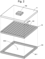
- a two-dimensional photonic-crystal laser 10 of the first example has a configuration in which a substrate 11, a first tunnel layer 121, a second tunnel layer 122, a p-type cladding layer (p-type semiconductor layer in the present invention) 131, an active layer 14, a carrier block layer 15, a two-dimensional photonic-crystal layer 16, an n-type cladding layer 132, and a contact layer 17 are sequentially stacked in order from the lower side of Fig. 1 .
- a lower side of the substrate 11 (opposite side of the first tunnel layer 121) is provided with a first electrode 181
- an upper side of the contact layer 17 opposite side of the n-type cladding layer 132
- a second electrode 182 is provided with a second electrode 182.
- the substrate 11 includes an n-type semiconductor
- the first tunnel layer 121 includes an n-type semiconductor higher in carrier (electron) density than that of the substrate 11.
- the p-type cladding layer 131 includes a p-type semiconductor
- the second tunnel layer 122 includes a p-type semiconductor higher in carrier (carrier hole) density than that of the p-type cladding layer 131.
- the active layer 14 generates light emission within a specific emission wavelength band upon being supplied with carrier holes and electrons.
- the active layer 14 includes, for example, a multiple-quantum well (MQW) in which a thin film including indium gallium arsenide (InGaAs) and a thin film including gallium arsenide (GaAs) are alternately stacked in large numbers.
- MQW multiple-quantum well
- the two-dimensional photonic-crystal layer 16 has a configuration in which a plurality of modified refractive index areas 162 are periodically arranged two-dimensionally in a plate-shaped base body 161 made of an n-type semiconductor.
- the modified refractive index areas 162 typically include holes (air), but members including a material other than the base body 161 may be used.
- the arrangement of the modified refractive index areas 162 has a square lattice shape in the example illustrated in Fig. 2 , but may have another shape such as a triangular lattice shape.
- the planar shape of the modified refractive index area 162 is an equilateral triangle in the example illustrated in Fig.
- one modified refractive index area 162 may be configured by combining a plurality of holes or a member including a material other than the base body 161.
- the carrier block layer 15, the n-type cladding layer 132, and the contact layer 17 each include an n-type semiconductor.
- the first electrode 181 is a plate-shaped conductor having a hollow portion formed inside, and has a frame portion 1811, which is a portion where the conductor remains, and a window portion 1812, which is the hollow portion of the conductor (see Fig. 2 ).
- the second electrode 182 includes a conductor plate provided at a position opposing the window portion 1812 of the first electrode 181 and having an area smaller than that of the window portion 1812 (see Fig. 2 ).
- n-type GaAs for the substrate 11
- n-type GaAs for example, 10 to 100 times
- p-type AlGaAs for the p-type cladding layer 131
- GaAs for example, 10 to 100 times
- n-type AlGaAs can be used for each of the carrier block layer 15, the base body 161 of the two-dimensional photonic-crystal layer 16, and the n-type cladding layer 132, and the impurity concentrations of these three layers may be the same or different.
- n-type GaAs can be used for the contact layer 17.
- the impurity concentration in each layer other than the first tunnel layer 121 and the second tunnel layer 122 is set to be (for example, 10 to 100 times) higher in each layer made of a p-type semiconductor than in each layer made of an n-type semiconductor.
- each layer described here is an example, and another p-type semiconductor can be used in each layer for which p-type GaAs or AlGaAs is exemplified, and another n-type semiconductor can be used in each layer for which n-type GaAs or AlGaAs is exemplified.
- These GaAs and AlGaAs can transmit light within a wavelength band of 0.7 to 1.0 ⁇ m.
- a semiconductor such as InP, GaN, or AlInGaAsP other than GaAs and AlGaAs may be used.
- the first tunnel layer 121 can be stacked by epitaxially growing on the substrate 11.
- each layer from the second tunnel layer 122 to the contact layer 17 can be stacked by epitaxially growing each layer of the immediate layer on the substrate 11 side.
- the first electrode 181 and the second electrode 182 can be made using a method such as a vapor deposition method with a metal such as gold as a material.
- the thickness of the substrate 11 is made sufficiently larger than the thickness of each layer from the first tunnel layer 121 to the contact layer 17. This makes the distance between the second electrode 182 and the active layer 14 sufficiently smaller than the distance between the first electrode 181 and the active layer 14.
- the thicknesses of the first tunnel layer 121 and the second tunnel layer 122 are made sufficiently smaller than the thicknesses of the respective layers from the substrate 11 and the p-type cladding layer 131 to the contact layer 17. This makes it easier for carrier holes supplied from the first electrode 181 as described later to easily reach the p-type cladding layer 131 (further, the active layer 14 via the p-type cladding layer 131).
- each layer is, for example, equal to or greater than 60 ⁇ m for the substrate 11, 10 to 2000 nm for the first tunnel layer 121, 10 to 2000 nm for the second tunnel layer 122, 1 to 10 ⁇ m for the p-type cladding layer 131, 1 to 100 nm for the active layer 14, 10 to 100 nm for the carrier block layer 15, 10 to 1000 nm for the two-dimensional photonic-crystal layer 16, 1 to 2 ⁇ m for the n-type cladding layer 132, and 10 to 500 nm for the contact layer 17.
- Carrier holes supplied from the first electrode 181 pass through the substrate 11, the first tunnel layer 121, the second tunnel layer 122, and the p-type cladding layer 131, and are introduced into the active layer 14.
- the substrate 11 and the first tunnel layer 121 include an n-type semiconductor
- the second tunnel layer 122 and the p-type cladding layer 131 includes a p-type semiconductor
- a reverse bias voltage that is positive on the n-type semiconductor side and negative on the p-type semiconductor side is applied at a boundary between the first tunnel layer 121 and the second tunnel layer 122.
- an electric current that crosses the boundary between an n-type semiconductor and a p-type semiconductor usually hardly flows.
- the impurity concentration of the first tunnel layer 121 is higher than that of the substrate 11 and the impurity concentration in the second tunnel layer 122 is higher than that of the p-type cladding layer 131, it becomes possible to achieve a state in which the carrier (electron) density in the first tunnel layer 121 and the carrier (carrier hole) density in the second tunnel layer 122 are high.
- This allows the carrier holes supplied from the first electrode 181 and introduced into the first tunnel layer 121 from the substrate 11 side to move to the second tunnel layer 122 by the tunnel effect, and are introduced into the active layer 14 from the second tunnel layer 122 through the p-type cladding layer 131.
- electrons supplied from the second electrode 182 are introduced into the active layer 14 through the contact layer 17, the two-dimensional photonic-crystal layer 16, and the carrier block layer 15. It should be noted that the carrier block layer 15 prevents carrier holes from moving from the active layer 14 to the two-dimensional photonic-crystal layer 16, and can cause electrons supplied from the two-dimensional photonic-crystal layer 16 side to move to the active layer 14.
- n-type GaAs can suppress the absorption coefficient of light in a case where the carrier density is the same to about 40% (in a case where the carrier density is 2 ⁇ 10 17 cm -3 ).
- use of n-type GaAs for the material of the base body 161 makes it possible to suppress absorption of light to about 1/3 to 1/5 as compared with the case of use of p-type GaAs.
- n-type GaAs is used as the material of the base body 161 as an example here, also when another n-type semiconductor such as AlGaAs is used as the material of the base body 161 (although numerical values are different), the carrier density and the absorption coefficient of light can be suppressed, and thus the same effects are achieved.
- the laser light thus generated is emitted from the window portion 1812 of the first electrode 181 to the outside.
- use of the n-type semiconductor as the material of the base body 161 of the two-dimensional photonic-crystal layer 16 makes it possible to suppress absorption of a portion of light by free carriers (electrons), and makes it possible to suppress decrease in the efficiency of laser oscillation.
- the base body 161 made of an n-type semiconductor since the base body 161 made of an n-type semiconductor is used, it is not necessary to use a substrate made of a p-type semiconductor, and it is possible to suppress the material cost by using the substrate 11 made of a less expensive n-type semiconductor.
- the active layer 14 having desired characteristics can be easily prepared without being affected by irregularities generated on the surface of the two-dimensional photonic-crystal layer 16.
- the substrate 11, the p-type cladding layer 131, the active layer 14, the carrier block layer 15, the two-dimensional photonic-crystal layer 16, the n-type cladding layer 132, and the contact layer 17 are similar to the respective constituent elements of the two-dimensional photonic-crystal laser 10 of the first example and thus description thereof is omitted.
- the first tunnel layer 121 includes an n-type semiconductor higher in carrier density than that of the substrate 11
- the second tunnel layer 122 includes a p-type semiconductor higher in carrier density than that of the p-type cladding layer 131.
- both the first tunnel layer 121 and the second tunnel layer 122 use an n-type semiconductor (first tunnel layer 121) and a p-type semiconductor (second tunnel layer 122) that are higher in carrier density than those in the first example
- first tunnel layer 121 n-type semiconductor
- second tunnel layer 122 p-type semiconductor
- InGaAs is a semiconductor that has a band gap smaller than that of GaAs or AlGaAs, and can thereby increase the carrier density.
- the first electrode 281 is provided on the lower face of the substrate 11, and the second electrode 282 is provided on the upper face of the contact layer 17.
- the first electrode 281 is larger in area than the second electrode 282.
- the first electrode 281 is provided on the entire lower face of the substrate 11, and the second electrode 282 is provided only near the center of the upper face of the contact layer 17.
- a material transparent with respect to laser light oscillated in the two-dimensional photonic-crystal layer 16 is used.
- a metal material such as gold can be used as the material of the first electrode 281, and indium tin oxide (ITO) can be used as the material of the second electrode 282.
- the laser light thus generated is emitted from each of the upper and lower faces of the two-dimensional photonic-crystal layer 16, and the laser light emitted to the first electrode 281 side among them is reflected by the reflection layer 21 and is directed toward the second electrode 282 side without entering the second tunnel layer 122 and the first tunnel layer 121. Therefore, the laser light emitted from any of the upper and lower faces of the two-dimensional photonic-crystal layer 16 is emitted to the outside directly from the upper face of the contact layer 17 or through the second electrode 182.
- the n-type semiconductor as the material of the base body 161 of the two-dimensional photonic-crystal layer 16 makes it possible to suppress absorption of a portion of light by free carriers (electrons), and makes it possible to suppress decrease in the efficiency of laser oscillation.
- the first tunnel layer 121 and the second tunnel layer 122 between the substrate 11 and the p-type cladding layer 131, it is possible to provide the base body 161 on the opposite side of the substrate 11 as viewed from the active layer 14 while using an n-type semiconductor for both the base body 161 and the substrate 11, it is possible to easily prepare the active layer 14 having desired characteristics without being affected by irregularities generated on the surface of the two-dimensional photonic-crystal layer 16.
- the reflection layer 21 is provided between the second tunnel layer 122 and the p-type cladding layer 131, laser light does not enter the first tunnel layer 121 and the second tunnel layer 122 higher in carrier density than other layers, and a portion of laser light can be prevented from being absorbed in the first tunnel layer 121 and the second tunnel layer 122.
- the carrier density supplied into the active layer 14 can be further increased and the intensity of the laser light can be further increased.
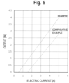
- Fig. 5 presents results of simulation of the device having the structure of Patent Literature 1 (A case where a base body made of a p-type semiconductor is used. Hereinafter, it is referred to as “comparative example”.) and the device having the structure of the second example (A case where a base body made of a n-type semiconductor is used, Hereinafter, it is referred to as “examples”. ).
- n-type semiconductor n-type GaAs
- p-type GaAs p-type semiconductor
- the in-plane loss (loss radiated to the outside of the device in the direction parallel to the plane) is calculated as 3 cm -1 in both the comparative example and the example, and the radiation coefficient is calculated as 12 cm -1 in the comparative example and 8 cm -1 in the example.
- the threshold electric current density is reduced from 0.6 kA ⁇ cm -2 (comparative example) to 0.2 kA ⁇ cm -2 (example), and the oscillation threshold electric current value has decreased.
- the slope efficiency is 0.79 W/A in the comparative example, whereas it is 0.88 W/A in the example.
- oscillation with a low threshold and operation with high slope efficiency become possible.
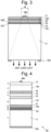
- Figs. 6A and 6B illustrate a schematic configuration of a two-dimensional photonic-crystal laser 30 of this embodiment.
- This two-dimensional photonic-crystal laser 30 is different from the two-dimensional photonic-crystal lasers 10 and 20 of the first and second examples in that a groove 32 is included, and a first electrode 381 is provided on a bottom face of the groove 32, and a reflection layer 31 is provided between the n-type cladding layer 132 and the contact layer 17.
- similar configurations to those of the two-dimensional photonic-crystal lasers 10 and 20 of the first and second examples will not be described, and only the above-described differences will be described.
- the groove 32 penetrates the reflection layer 31, the n-type cladding layer 132, the two-dimensional photonic-crystal layer 16, the carrier block layer 15, the active layer 14, the p-type cladding layer 131, the second tunnel layer 122, and the first tunnel layer 121 from the surface of the contact layer 17, and is dug down to a position between the upper face and the lower face of the substrate 11.
- the shape (planar shape) of the groove 32 in a cross section parallel to the two-dimensional photonic-crystal layer 16 (the same applies to other layers such as the contact layer 17) is a frame shape.
- the shape of the first electrode 381 provided on the bottom face of the groove 32 is a frame shape similar to the planar shape of the groove 32, and is similar to the shape of the frame portion 1811 of the first electrode 181 in the first example. Since the first electrode 381 is provided on the bottom face of the groove 32 in this manner, the position of the first electrode 381 in the vertical direction is a position between the upper face and the lower face of the substrate 11.
- the reflection layer 31 is provided between the n-type cladding layer 132 and the contact layer 17 as described above.
- the reflection layer 31 similarly to the reflection layer 21 in the second example, one including DBR can be used.
- the planar shape of the first electrode 381 is a frame shape, the laser light passes through inside the frame of the first electrode 381 and is emitted from the surface of the substrate 11 to the outside. Therefore, it is possible to suppress the first electrode 381 from hindering emission of laser light and causing unnecessary diffraction.
- the two-dimensional photonic-crystal laser 30 of an embodiment can be easily prepared in the following points.
- each layer such as the second tunnel layer 122 is prepared on the upper face of the substrate 11 and the first electrodes 181 and 281 are prepared on the lower face, it is necessary to invert the upper and lower sides of the substrate 11 between the preparation of each layer and the preparation of the first electrodes 181 and 281.
- each layer such as the second tunnel layer 122 and the first electrode 381 are prepared on the upper face of the substrate 11, it is not necessary to invert the upper and lower sides of the substrate 11, and manufacturing becomes easy.
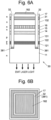
- an n-type semiconductor is used as the material of the base body 161, but in order to further suppress the absorption loss of light due to free carriers, as illustrated in Fig. 7A , a non-carrier-doped semiconductor (described as "i" in the figure) may be used as the material of a base body 161A of a two-dimensional photonic-crystal layer 16A.
- a non-carrier-doped semiconductor (described as "i" in the figure) may be used as the material of a base body 161A of a two-dimensional photonic-crystal layer 16A.
- an n-type semiconductor may be used for a portion 1611 (in one example, 30% in area ratio) of a base body 161B of a two-dimensional photonic-crystal layer 16B, and a non-carrier-doped semiconductor may be used for a remaining portion 1612 (in the one example, 70% in area ratio).
- the second electrode 282 smaller in area than the first electrode 281 is provided near the center of the upper face of the contact layer 17, but instead, a window-shaped electrode having a frame portion and a window portion similar to those of the first electrode 181 in the first example may be provided on the upper face of the contact layer 17 as the second electrode.
- a window-shaped electrode having a frame portion and a window portion similar to those of the first electrode 181 in the first example may be provided on the upper face of the contact layer 17 as the second electrode.
- providing a window-shaped electrode to the other electrode makes it difficult to supply charges near the center of the two-dimensional photonic-crystal layer.
- n-type semiconductor for the cladding layer (n-type cladding layer 132) provided between the second electrode 282 and the two-dimensional photonic-crystal layer 16 and the contact layer 17 makes it possible to increase the mobility of charges (electrons). Therefore, even if a window-shaped electrode is used for the second electrode 282, it is possible to supply charges near the center of the two-dimensional photonic-crystal layer 16.
- the first electrode 381 is provided on the bottom face of the groove 32, and the reflection layer 31 is provided between the n-type cladding layer 132 and the contact layer 17.
- the reflection layer 21 may be provided between the second tunnel layer 122 and the p-type cladding layer 131 in place of the reflection layer 31.
- the first electrode 181 may be provided on the lower face of the substrate 11 without providing the groove 32 and the first electrode 381 on the bottom face of the groove 32.
Landscapes
- Physics & Mathematics (AREA)
- Condensed Matter Physics & Semiconductors (AREA)
- General Physics & Mathematics (AREA)
- Electromagnetism (AREA)
- Optics & Photonics (AREA)
- Geometry (AREA)
- Semiconductor Lasers (AREA)
Claims (5)
- Laser à cristal photonique bidimensionnel (10 ; 20 ; 30) comprenant :a) un substrat (11) constitué d'un semi-conducteur de type n ;b) une couche de semi-conducteur de type p (131) ménagée sur un côté supérieur du substrat (11) et constituée d'un semi-conducteur de type p ;c) une couche active (14) ménagée sur un côté supérieur de la couche de semi-conducteur de type p (131) ;d) une couche de cristal photonique bidimensionnel (16 ; 16A ; 16B) ménagée sur un côté supérieur de la couche active (14) et comportant un corps de base (161 ; 161A ; 161B) en forme de plaque constitué d'un semi-conducteur de type n dans lequel des zones à indice de réfraction modifié (162) dont l'indice de réfraction diffère du corps de base (161 ; 161A ; 161B) sont agencées périodiquement ;e) une première couche tunnel (121) ménagée entre le substrat (11) et la couche de semi-conducteur de type p (131) et constituée d'un semi-conducteur de type n ayant une densité de porteurs supérieure à une densité de porteurs du substrat (11) ;f) une seconde couche tunnel (122) ménagée en contact avec la première couche tunnel (121) entre la première couche tunnel (121) et la couche de semi-conducteur de type p (131), et constituée d'un semi-conducteur de type p ayant une densité de porteurs supérieure à une densité de porteurs de la couche de semi-conducteur de type p (131) ;g) une première électrode (181 ; 281 ; 381) ménagée sur un côté inférieur du substrat (11) ou dans le substrat (11) ;h) une seconde électrode (182 ; 282) ménagée sur un côté supérieur de la couche de cristal photonique bidimensionnel (16 ; 16A ; 16B) ; eti) une rainure (32) ménagée à partir d'une surface sur un côté supérieur du laser à cristal photonique bidimensionnel (10 ; 20 ; 30), ayant une face de fond à une position entre une face supérieure et une face inférieure du substrat (11), et ayant une forme de type cadre dans une section transversale parallèle à la couche de cristal photonique bidimensionnel (16, 16A, 16B),dans lequel la première électrode (181 ; 281 ; 381) est ménagée sur la face de fond de la rainure (32).
- Laser à cristal photonique bidimensionnel (10 ; 20 ; 30) selon la revendication 1 comprenant en outre une couche de réflexion (21 ; 31) configurée pour réfléchir une lumière laser générée dans la couche de cristal photonique bidimensionnel (16 ; 16A ; 16B) entre la seconde couche tunnel (122) et la couche de semi-conducteur de type p (131).
- Laser à cristal photonique bidimensionnel (10 ; 20 ; 30) selon la revendication 1 comprenant en outre une couche de réflexion (21 ; 31) configurée pour réfléchir une lumière laser générée dans la couche de cristal photonique bidimensionnel (16 ; 16A ; 16B) entre la couche de cristal photonique bidimensionnel (16 ; 16A ; 16B) et la seconde électrode (181 ; 182).
- Laser à cristal photonique bidimensionnel (10 ; 20 ; 30) selon la revendication 1 ou 2, dans lequel des matériaux du substrat (11) et du corps de base (161 ; 161A ; 161B) de la couche de cristal photonique bidimensionnel (16 ; 16A ; 16B) sont GaAs de type n ou AlGaAs de type n,un matériau de la couche de semi-conducteur de type p (131) est GaAs de type p ou AlGaAs de type p,un matériau de la première couche tunnel (121) est InGaAs de type n, etun matériau de la seconde couche tunnel (122) est InGaAs de type p.
- Laser à cristal photonique bidimensionnel (10 ; 20 ; 30) selon l'une quelconque des revendications 1 à 3, dans lequel la totalité ou une partie du corps de base (161 ; 161A ; 161B) est constituée d'un semi-conducteur non dopé en porteurs à la place d'un semi-conducteur de type n.
Applications Claiming Priority (2)
| Application Number | Priority Date | Filing Date | Title |
|---|---|---|---|
| JP2020062586 | 2020-03-31 | ||
| PCT/JP2021/010882 WO2021200168A1 (fr) | 2020-03-31 | 2021-03-17 | Laser à cristal photonique bidimensionnel |
Publications (3)
| Publication Number | Publication Date |
|---|---|
| EP4131677A1 EP4131677A1 (fr) | 2023-02-08 |
| EP4131677A4 EP4131677A4 (fr) | 2023-11-01 |
| EP4131677B1 true EP4131677B1 (fr) | 2025-03-05 |
Family
ID=77928198
Family Applications (1)
| Application Number | Title | Priority Date | Filing Date |
|---|---|---|---|
| EP21781958.0A Active EP4131677B1 (fr) | 2020-03-31 | 2021-03-17 | Laser à cristal photonique bidimensionnel |
Country Status (5)
| Country | Link |
|---|---|
| US (1) | US12489271B2 (fr) |
| EP (1) | EP4131677B1 (fr) |
| JP (1) | JP7689112B2 (fr) |
| CN (1) | CN115398761B (fr) |
| WO (1) | WO2021200168A1 (fr) |
Families Citing this family (4)
| Publication number | Priority date | Publication date | Assignee | Title |
|---|---|---|---|---|
| US20250047063A1 (en) * | 2022-02-08 | 2025-02-06 | Ams-Osram International Gmbh | Laser diode component |
| CN119836718A (zh) * | 2022-08-25 | 2025-04-15 | 国立大学法人京都大学 | 二维光子晶体激光器 |
| CN115995757B (zh) * | 2023-03-23 | 2023-06-16 | 香港中文大学(深圳) | 一种光子晶体电泵浦表面发射激光器及其制备方法 |
| DE102023116537A1 (de) * | 2023-06-23 | 2024-12-24 | Ams-Osram International Gmbh | Verfahren zur herstellung einer vielzahl an halbleiterlaserchip, halbleiterlaserchip, verfahren zur herstellung eines laserbauelements und laserbauelement |
Family Cites Families (31)
| Publication number | Priority date | Publication date | Assignee | Title |
|---|---|---|---|---|
| JP2002368334A (ja) * | 2001-03-26 | 2002-12-20 | Seiko Epson Corp | 面発光レーザ、フォトダイオード、それらの製造方法及びそれらを用いた光電気混載回路 |
| US6687268B2 (en) | 2001-03-26 | 2004-02-03 | Seiko Epson Corporation | Surface emitting laser and photodiode, manufacturing method therefor, and optoelectric integrated circuit using the surface emitting laser and the photodiode |
| US7123638B2 (en) * | 2003-10-17 | 2006-10-17 | Avago Technologies General Ip (Singapore) Pte. Ltd. | Tunnel-junction structure incorporating N-type layer comprising nitrogen and a group VI dopant |
| JP2005277026A (ja) * | 2004-03-24 | 2005-10-06 | Fuji Photo Film Co Ltd | 半導体レーザ素子 |
| US7483466B2 (en) * | 2005-04-28 | 2009-01-27 | Canon Kabushiki Kaisha | Vertical cavity surface emitting laser device |
| JP2007189080A (ja) * | 2006-01-13 | 2007-07-26 | Fujitsu Ltd | 光半導体装置 |
| US8124957B2 (en) * | 2006-02-22 | 2012-02-28 | Cree, Inc. | Low resistance tunnel junctions in wide band gap materials and method of making same |
| JP2007234824A (ja) * | 2006-02-28 | 2007-09-13 | Canon Inc | 垂直共振器型面発光レーザ |
| JP4793820B2 (ja) | 2006-03-20 | 2011-10-12 | 国立大学法人京都大学 | 2次元フォトニック結晶面発光レーザ光源 |
| JP4948012B2 (ja) * | 2006-03-24 | 2012-06-06 | 古河電気工業株式会社 | 面発光レーザ素子および面発光レーザ素子の製造方法 |
| JP2007273849A (ja) * | 2006-03-31 | 2007-10-18 | Canon Inc | 垂直共振器型面発光レーザ |
| JP2008226884A (ja) * | 2007-03-08 | 2008-09-25 | Canon Inc | n型の13族窒化物半導体の製造方法、面発光レーザ、面発光レーザにおける電流狭窄構造の製造方法、窒化物半導体の抵抗を変化させる方法、及び半導体レーザの製造方法 |
| JP4350774B2 (ja) * | 2007-07-31 | 2009-10-21 | キヤノン株式会社 | 面発光レーザ |
| JP2009054789A (ja) * | 2007-08-27 | 2009-03-12 | Sumitomo Electric Ind Ltd | 半導体レーザ素子の製造方法 |
| KR101017809B1 (ko) * | 2008-03-13 | 2011-02-28 | 주식회사 하이닉스반도체 | 반도체 소자 및 그 제조 방법 |
| JP2010093127A (ja) * | 2008-10-09 | 2010-04-22 | Sumitomo Electric Ind Ltd | 半導体発光装置 |
| JP5854417B2 (ja) | 2010-07-30 | 2016-02-09 | 国立大学法人京都大学 | 2次元フォトニック結晶レーザ |
| DE112011102431B4 (de) * | 2010-10-04 | 2014-03-06 | Furukawa Electric Co., Ltd., | Elektronische Einrichtung, flächenemittierender Laser, flächenemittierendes Laser-Array, Lichtquelle, optisches Modul |
| JP2012119408A (ja) * | 2010-11-30 | 2012-06-21 | Nippon Telegr & Teleph Corp <Ntt> | 半導体素子、半導体光素子及び半導体集積素子 |
| US8653550B2 (en) | 2010-12-17 | 2014-02-18 | The United States Of America, As Represented By The Secretary Of The Navy | Inverted light emitting diode having plasmonically enhanced emission |
| JP5678806B2 (ja) * | 2011-06-07 | 2015-03-04 | 株式会社デンソー | 半導体レーザ及びその製造方法 |
| JP5794687B2 (ja) * | 2011-08-12 | 2015-10-14 | 国立大学法人京都大学 | フォトニック結晶面発光レーザ |
| JP2013161965A (ja) * | 2012-02-06 | 2013-08-19 | Kyoto Univ | 半導体発光素子 |
| JP6013948B2 (ja) * | 2013-03-13 | 2016-10-25 | ルネサスエレクトロニクス株式会社 | 半導体装置 |
| WO2017038595A1 (fr) * | 2015-08-28 | 2017-03-09 | 国立大学法人京都大学 | Laser émettant en surface à cristal photonique bidimensionnel |
| US11031751B2 (en) * | 2016-08-10 | 2021-06-08 | Hamamatsu Photonics K.K. | Light-emitting device |
| JP6868864B2 (ja) | 2017-03-06 | 2021-05-12 | スタンレー電気株式会社 | 照明装置 |
| JP6355178B2 (ja) * | 2017-06-29 | 2018-07-11 | 国立大学法人京都大学 | レーザ装置 |
| JP6947386B2 (ja) | 2017-06-29 | 2021-10-13 | 学校法人 名城大学 | 半導体発光素子および半導体発光素子の製造方法 |
| JP6951890B2 (ja) * | 2017-07-10 | 2021-10-20 | 浜松ホトニクス株式会社 | 半導体レーザ素子 |
| WO2019152611A1 (fr) | 2018-02-02 | 2019-08-08 | Cornell University | Plates-formes activées par jonction tunnel enterrée pour systèmes photoniques et électroniques intégrés |
-
2021
- 2021-03-17 EP EP21781958.0A patent/EP4131677B1/fr active Active
- 2021-03-17 WO PCT/JP2021/010882 patent/WO2021200168A1/fr not_active Ceased
- 2021-03-17 CN CN202180025967.3A patent/CN115398761B/zh active Active
- 2021-03-17 US US17/908,202 patent/US12489271B2/en active Active
- 2021-03-17 JP JP2022511852A patent/JP7689112B2/ja active Active
Also Published As
| Publication number | Publication date |
|---|---|
| EP4131677A1 (fr) | 2023-02-08 |
| EP4131677A4 (fr) | 2023-11-01 |
| US12489271B2 (en) | 2025-12-02 |
| JP7689112B2 (ja) | 2025-06-05 |
| CN115398761B (zh) | 2025-09-30 |
| US20230361530A1 (en) | 2023-11-09 |
| WO2021200168A1 (fr) | 2021-10-07 |
| JPWO2021200168A1 (fr) | 2021-10-07 |
| CN115398761A (zh) | 2022-11-25 |
Similar Documents
| Publication | Publication Date | Title |
|---|---|---|
| EP4131677B1 (fr) | Laser à cristal photonique bidimensionnel | |
| EP0975073B1 (fr) | Laser à semi-conducteur | |
| US12538612B2 (en) | Light-emitting diode element | |
| JP2004071896A (ja) | 発光素子の製造方法及び発光素子 | |
| US20230395745A1 (en) | Light emitting diode element | |
| TWI758822B (zh) | 半導體裝置 | |
| US4759025A (en) | Window structure semiconductor laser | |
| JP4930317B2 (ja) | 半導体光素子 | |
| JP4696749B2 (ja) | 半導体発光素子 | |
| JPS60145687A (ja) | 半導体レ−ザ− | |
| CN115425518A (zh) | 一种半导体激光器及光学设备 | |
| US11881674B2 (en) | Surface-emitting semiconductor light-emitting device | |
| US20240313507A1 (en) | Vertical cavity surface emitting laser device, vertical cavity surface emitting laser device array, and method of producing a vertical cavity surface emitting laser device | |
| JP2876642B2 (ja) | 量子井戸レーザ | |
| JPH03174793A (ja) | 半導体レーザ | |
| JPS61224482A (ja) | 半導体発光装置 | |
| JP2025107007A (ja) | 面発光型レーザ、及び、その製造方法 | |
| JP2000164990A (ja) | 半導体レーザ | |
| JP2014154798A (ja) | 半導体レーザ素子及びレーザモジュール | |
| JPS6016488A (ja) | 半導体レ−ザ装置 | |
| JPH054833B2 (fr) | ||
| JP2007013100A (ja) | 半導体レーザ | |
| JPH04260377A (ja) | 化合物光半導体装置 | |
| JP2001077475A (ja) | 半導体レーザ | |
| JPS60134489A (ja) | 半導体レ−ザ装置 |
Legal Events
| Date | Code | Title | Description |
|---|---|---|---|
| STAA | Information on the status of an ep patent application or granted ep patent |
Free format text: STATUS: THE INTERNATIONAL PUBLICATION HAS BEEN MADE |
|
| PUAI | Public reference made under article 153(3) epc to a published international application that has entered the european phase |
Free format text: ORIGINAL CODE: 0009012 |
|
| STAA | Information on the status of an ep patent application or granted ep patent |
Free format text: STATUS: REQUEST FOR EXAMINATION WAS MADE |
|
| 17P | Request for examination filed |
Effective date: 20221021 |
|
| AK | Designated contracting states |
Kind code of ref document: A1 Designated state(s): AL AT BE BG CH CY CZ DE DK EE ES FI FR GB GR HR HU IE IS IT LI LT LU LV MC MK MT NL NO PL PT RO RS SE SI SK SM TR |
|
| DAV | Request for validation of the european patent (deleted) | ||
| DAX | Request for extension of the european patent (deleted) | ||
| REG | Reference to a national code |
Ref country code: DE Ref legal event code: R079 Free format text: PREVIOUS MAIN CLASS: H01S0005183000 Ipc: H01S0005185000 Ref country code: DE Ref legal event code: R079 Ref document number: 602021027230 Country of ref document: DE Free format text: PREVIOUS MAIN CLASS: H01S0005183000 Ipc: H01S0005185000 |
|
| A4 | Supplementary search report drawn up and despatched |
Effective date: 20230929 |
|
| RIC1 | Information provided on ipc code assigned before grant |
Ipc: H01S 5/343 20060101ALN20230925BHEP Ipc: H01S 5/042 20060101ALI20230925BHEP Ipc: H01S 5/11 20210101ALI20230925BHEP Ipc: H01S 5/185 20210101AFI20230925BHEP |
|
| GRAP | Despatch of communication of intention to grant a patent |
Free format text: ORIGINAL CODE: EPIDOSNIGR1 |
|
| STAA | Information on the status of an ep patent application or granted ep patent |
Free format text: STATUS: GRANT OF PATENT IS INTENDED |
|
| RIC1 | Information provided on ipc code assigned before grant |
Ipc: H01S 5/343 20060101ALN20240722BHEP Ipc: H01S 5/042 20060101ALI20240722BHEP Ipc: H01S 5/11 20210101ALI20240722BHEP Ipc: H01S 5/185 20210101AFI20240722BHEP |
|
| INTG | Intention to grant announced |
Effective date: 20240805 |
|
| GRAJ | Information related to disapproval of communication of intention to grant by the applicant or resumption of examination proceedings by the epo deleted |
Free format text: ORIGINAL CODE: EPIDOSDIGR1 |
|
| STAA | Information on the status of an ep patent application or granted ep patent |
Free format text: STATUS: REQUEST FOR EXAMINATION WAS MADE |
|
| INTC | Intention to grant announced (deleted) | ||
| GRAP | Despatch of communication of intention to grant a patent |
Free format text: ORIGINAL CODE: EPIDOSNIGR1 |
|
| STAA | Information on the status of an ep patent application or granted ep patent |
Free format text: STATUS: GRANT OF PATENT IS INTENDED |
|
| GRAS | Grant fee paid |
Free format text: ORIGINAL CODE: EPIDOSNIGR3 |
|
| GRAA | (expected) grant |
Free format text: ORIGINAL CODE: 0009210 |
|
| STAA | Information on the status of an ep patent application or granted ep patent |
Free format text: STATUS: THE PATENT HAS BEEN GRANTED |
|
| P01 | Opt-out of the competence of the unified patent court (upc) registered |
Free format text: CASE NUMBER: APP_1660/2025 Effective date: 20250110 |
|
| RIC1 | Information provided on ipc code assigned before grant |
Ipc: H01S 5/343 20060101ALN20250113BHEP Ipc: H01S 5/042 20060101ALI20250113BHEP Ipc: H01S 5/11 20210101ALI20250113BHEP Ipc: H01S 5/185 20210101AFI20250113BHEP |
|
| INTG | Intention to grant announced |
Effective date: 20250122 |
|
| AK | Designated contracting states |
Kind code of ref document: B1 Designated state(s): AL AT BE BG CH CY CZ DE DK EE ES FI FR GB GR HR HU IE IS IT LI LT LU LV MC MK MT NL NO PL PT RO RS SE SI SK SM TR |
|
| REG | Reference to a national code |
Ref country code: GB Ref legal event code: FG4D |
|
| REG | Reference to a national code |
Ref country code: CH Ref legal event code: EP |
|
| REG | Reference to a national code |
Ref country code: IE Ref legal event code: FG4D |
|
| REG | Reference to a national code |
Ref country code: DE Ref legal event code: R096 Ref document number: 602021027230 Country of ref document: DE |
|
| PGFP | Annual fee paid to national office [announced via postgrant information from national office to epo] |
Ref country code: AT Payment date: 20250417 Year of fee payment: 5 |
|
| PG25 | Lapsed in a contracting state [announced via postgrant information from national office to epo] |
Ref country code: RS Free format text: LAPSE BECAUSE OF FAILURE TO SUBMIT A TRANSLATION OF THE DESCRIPTION OR TO PAY THE FEE WITHIN THE PRESCRIBED TIME-LIMIT Effective date: 20250605 |
|
| PG25 | Lapsed in a contracting state [announced via postgrant information from national office to epo] |
Ref country code: FI Free format text: LAPSE BECAUSE OF FAILURE TO SUBMIT A TRANSLATION OF THE DESCRIPTION OR TO PAY THE FEE WITHIN THE PRESCRIBED TIME-LIMIT Effective date: 20250305 |
|
| REG | Reference to a national code |
Ref country code: NL Ref legal event code: MP Effective date: 20250305 |
|
| PG25 | Lapsed in a contracting state [announced via postgrant information from national office to epo] |
Ref country code: ES Free format text: LAPSE BECAUSE OF FAILURE TO SUBMIT A TRANSLATION OF THE DESCRIPTION OR TO PAY THE FEE WITHIN THE PRESCRIBED TIME-LIMIT Effective date: 20250305 |
|
| REG | Reference to a national code |
Ref country code: LT Ref legal event code: MG9D |
|
| PG25 | Lapsed in a contracting state [announced via postgrant information from national office to epo] |
Ref country code: NO Free format text: LAPSE BECAUSE OF FAILURE TO SUBMIT A TRANSLATION OF THE DESCRIPTION OR TO PAY THE FEE WITHIN THE PRESCRIBED TIME-LIMIT Effective date: 20250605 |
|
| PG25 | Lapsed in a contracting state [announced via postgrant information from national office to epo] |
Ref country code: HR Free format text: LAPSE BECAUSE OF FAILURE TO SUBMIT A TRANSLATION OF THE DESCRIPTION OR TO PAY THE FEE WITHIN THE PRESCRIBED TIME-LIMIT Effective date: 20250305 |
|
| PG25 | Lapsed in a contracting state [announced via postgrant information from national office to epo] |
Ref country code: LV Free format text: LAPSE BECAUSE OF FAILURE TO SUBMIT A TRANSLATION OF THE DESCRIPTION OR TO PAY THE FEE WITHIN THE PRESCRIBED TIME-LIMIT Effective date: 20250305 |
|
| PG25 | Lapsed in a contracting state [announced via postgrant information from national office to epo] |
Ref country code: BG Free format text: LAPSE BECAUSE OF FAILURE TO SUBMIT A TRANSLATION OF THE DESCRIPTION OR TO PAY THE FEE WITHIN THE PRESCRIBED TIME-LIMIT Effective date: 20250305 Ref country code: GR Free format text: LAPSE BECAUSE OF FAILURE TO SUBMIT A TRANSLATION OF THE DESCRIPTION OR TO PAY THE FEE WITHIN THE PRESCRIBED TIME-LIMIT Effective date: 20250606 |
|
| REG | Reference to a national code |
Ref country code: AT Ref legal event code: MK05 Ref document number: 1773854 Country of ref document: AT Kind code of ref document: T Effective date: 20250305 |
|
| PG25 | Lapsed in a contracting state [announced via postgrant information from national office to epo] |
Ref country code: NL Free format text: LAPSE BECAUSE OF FAILURE TO SUBMIT A TRANSLATION OF THE DESCRIPTION OR TO PAY THE FEE WITHIN THE PRESCRIBED TIME-LIMIT Effective date: 20250305 |
|
| PG25 | Lapsed in a contracting state [announced via postgrant information from national office to epo] |
Ref country code: SE Free format text: LAPSE BECAUSE OF FAILURE TO SUBMIT A TRANSLATION OF THE DESCRIPTION OR TO PAY THE FEE WITHIN THE PRESCRIBED TIME-LIMIT Effective date: 20250305 |
|
| PG25 | Lapsed in a contracting state [announced via postgrant information from national office to epo] |
Ref country code: SM Free format text: LAPSE BECAUSE OF FAILURE TO SUBMIT A TRANSLATION OF THE DESCRIPTION OR TO PAY THE FEE WITHIN THE PRESCRIBED TIME-LIMIT Effective date: 20250305 |
|
| PG25 | Lapsed in a contracting state [announced via postgrant information from national office to epo] |
Ref country code: PT Free format text: LAPSE BECAUSE OF FAILURE TO SUBMIT A TRANSLATION OF THE DESCRIPTION OR TO PAY THE FEE WITHIN THE PRESCRIBED TIME-LIMIT Effective date: 20250707 |
|
| PG25 | Lapsed in a contracting state [announced via postgrant information from national office to epo] |
Ref country code: IT Free format text: LAPSE BECAUSE OF FAILURE TO SUBMIT A TRANSLATION OF THE DESCRIPTION OR TO PAY THE FEE WITHIN THE PRESCRIBED TIME-LIMIT Effective date: 20250305 Ref country code: PL Free format text: LAPSE BECAUSE OF FAILURE TO SUBMIT A TRANSLATION OF THE DESCRIPTION OR TO PAY THE FEE WITHIN THE PRESCRIBED TIME-LIMIT Effective date: 20250305 |
|
| PG25 | Lapsed in a contracting state [announced via postgrant information from national office to epo] |
Ref country code: AT Free format text: LAPSE BECAUSE OF FAILURE TO SUBMIT A TRANSLATION OF THE DESCRIPTION OR TO PAY THE FEE WITHIN THE PRESCRIBED TIME-LIMIT Effective date: 20250305 |
|
| PG25 | Lapsed in a contracting state [announced via postgrant information from national office to epo] |
Ref country code: CZ Free format text: LAPSE BECAUSE OF FAILURE TO SUBMIT A TRANSLATION OF THE DESCRIPTION OR TO PAY THE FEE WITHIN THE PRESCRIBED TIME-LIMIT Effective date: 20250305 Ref country code: EE Free format text: LAPSE BECAUSE OF FAILURE TO SUBMIT A TRANSLATION OF THE DESCRIPTION OR TO PAY THE FEE WITHIN THE PRESCRIBED TIME-LIMIT Effective date: 20250305 |
|
| REG | Reference to a national code |
Ref country code: CH Ref legal event code: H13 Free format text: ST27 STATUS EVENT CODE: U-0-0-H10-H13 (AS PROVIDED BY THE NATIONAL OFFICE) Effective date: 20251023 |
|
| PG25 | Lapsed in a contracting state [announced via postgrant information from national office to epo] |
Ref country code: RO Free format text: LAPSE BECAUSE OF FAILURE TO SUBMIT A TRANSLATION OF THE DESCRIPTION OR TO PAY THE FEE WITHIN THE PRESCRIBED TIME-LIMIT Effective date: 20250305 |
|
| PG25 | Lapsed in a contracting state [announced via postgrant information from national office to epo] |
Ref country code: SK Free format text: LAPSE BECAUSE OF FAILURE TO SUBMIT A TRANSLATION OF THE DESCRIPTION OR TO PAY THE FEE WITHIN THE PRESCRIBED TIME-LIMIT Effective date: 20250305 |
|
| PG25 | Lapsed in a contracting state [announced via postgrant information from national office to epo] |
Ref country code: IS Free format text: LAPSE BECAUSE OF FAILURE TO SUBMIT A TRANSLATION OF THE DESCRIPTION OR TO PAY THE FEE WITHIN THE PRESCRIBED TIME-LIMIT Effective date: 20250705 |
|
| PG25 | Lapsed in a contracting state [announced via postgrant information from national office to epo] |
Ref country code: LU Free format text: LAPSE BECAUSE OF NON-PAYMENT OF DUE FEES Effective date: 20250317 |
|
| REG | Reference to a national code |
Ref country code: DE Ref legal event code: R097 Ref document number: 602021027230 Country of ref document: DE |
|
| REG | Reference to a national code |
Ref country code: BE Ref legal event code: MM Effective date: 20250331 |
|
| PG25 | Lapsed in a contracting state [announced via postgrant information from national office to epo] |
Ref country code: MC Free format text: LAPSE BECAUSE OF FAILURE TO SUBMIT A TRANSLATION OF THE DESCRIPTION OR TO PAY THE FEE WITHIN THE PRESCRIBED TIME-LIMIT Effective date: 20250305 |
|
| PLBE | No opposition filed within time limit |
Free format text: ORIGINAL CODE: 0009261 |
|
| STAA | Information on the status of an ep patent application or granted ep patent |
Free format text: STATUS: NO OPPOSITION FILED WITHIN TIME LIMIT |
|
| PG25 | Lapsed in a contracting state [announced via postgrant information from national office to epo] |
Ref country code: DK Free format text: LAPSE BECAUSE OF FAILURE TO SUBMIT A TRANSLATION OF THE DESCRIPTION OR TO PAY THE FEE WITHIN THE PRESCRIBED TIME-LIMIT Effective date: 20250305 |
|
| REG | Reference to a national code |
Ref country code: CH Ref legal event code: L10 Free format text: ST27 STATUS EVENT CODE: U-0-0-L10-L00 (AS PROVIDED BY THE NATIONAL OFFICE) Effective date: 20260114 |
|
| PG25 | Lapsed in a contracting state [announced via postgrant information from national office to epo] |
Ref country code: BE Free format text: LAPSE BECAUSE OF NON-PAYMENT OF DUE FEES Effective date: 20250331 |
|
| PG25 | Lapsed in a contracting state [announced via postgrant information from national office to epo] |
Ref country code: CH Free format text: LAPSE BECAUSE OF NON-PAYMENT OF DUE FEES Effective date: 20250331 |
|
| PG25 | Lapsed in a contracting state [announced via postgrant information from national office to epo] |
Ref country code: IE Free format text: LAPSE BECAUSE OF NON-PAYMENT OF DUE FEES Effective date: 20250317 |
|
| 26N | No opposition filed |
Effective date: 20251208 |
|
| PGFP | Annual fee paid to national office [announced via postgrant information from national office to epo] |
Ref country code: GB Payment date: 20260128 Year of fee payment: 6 |
|
| PGFP | Annual fee paid to national office [announced via postgrant information from national office to epo] |
Ref country code: DE Payment date: 20260122 Year of fee payment: 6 |
|
| PG25 | Lapsed in a contracting state [announced via postgrant information from national office to epo] |
Ref country code: FR Free format text: LAPSE BECAUSE OF NON-PAYMENT OF DUE FEES Effective date: 20250505 |