EP4131758A1 - Système de convertisseur résonant avec démarrage en douceur et commande de tension de sortie et son procédé de commande - Google Patents
Système de convertisseur résonant avec démarrage en douceur et commande de tension de sortie et son procédé de commande Download PDFInfo
- Publication number
- EP4131758A1 EP4131758A1 EP21382739.7A EP21382739A EP4131758A1 EP 4131758 A1 EP4131758 A1 EP 4131758A1 EP 21382739 A EP21382739 A EP 21382739A EP 4131758 A1 EP4131758 A1 EP 4131758A1
- Authority
- EP
- European Patent Office
- Prior art keywords
- during
- cycle
- duty
- time interval
- resonant converter
- Prior art date
- Legal status (The legal status is an assumption and is not a legal conclusion. Google has not performed a legal analysis and makes no representation as to the accuracy of the status listed.)
- Pending
Links
Images

Classifications
-
- H—ELECTRICITY
- H02—GENERATION; CONVERSION OR DISTRIBUTION OF ELECTRIC POWER
- H02M—APPARATUS FOR CONVERSION BETWEEN AC AND AC, BETWEEN AC AND DC, OR BETWEEN DC AND DC, AND FOR USE WITH MAINS OR SIMILAR POWER SUPPLY SYSTEMS; CONVERSION OF DC OR AC INPUT POWER INTO SURGE OUTPUT POWER; CONTROL OR REGULATION THEREOF
- H02M1/00—Details of apparatus for conversion
- H02M1/36—Means for starting or stopping converters
-
- H—ELECTRICITY
- H02—GENERATION; CONVERSION OR DISTRIBUTION OF ELECTRIC POWER
- H02M—APPARATUS FOR CONVERSION BETWEEN AC AND AC, BETWEEN AC AND DC, OR BETWEEN DC AND DC, AND FOR USE WITH MAINS OR SIMILAR POWER SUPPLY SYSTEMS; CONVERSION OF DC OR AC INPUT POWER INTO SURGE OUTPUT POWER; CONTROL OR REGULATION THEREOF
- H02M3/00—Conversion of DC power input into DC power output
- H02M3/01—Resonant DC/DC converters
-
- H—ELECTRICITY
- H02—GENERATION; CONVERSION OR DISTRIBUTION OF ELECTRIC POWER
- H02M—APPARATUS FOR CONVERSION BETWEEN AC AND AC, BETWEEN AC AND DC, OR BETWEEN DC AND DC, AND FOR USE WITH MAINS OR SIMILAR POWER SUPPLY SYSTEMS; CONVERSION OF DC OR AC INPUT POWER INTO SURGE OUTPUT POWER; CONTROL OR REGULATION THEREOF
- H02M3/00—Conversion of DC power input into DC power output
- H02M3/22—Conversion of DC power input into DC power output with intermediate conversion into AC
-
- Y—GENERAL TAGGING OF NEW TECHNOLOGICAL DEVELOPMENTS; GENERAL TAGGING OF CROSS-SECTIONAL TECHNOLOGIES SPANNING OVER SEVERAL SECTIONS OF THE IPC; TECHNICAL SUBJECTS COVERED BY FORMER USPC CROSS-REFERENCE ART COLLECTIONS [XRACs] AND DIGESTS
- Y02—TECHNOLOGIES OR APPLICATIONS FOR MITIGATION OR ADAPTATION AGAINST CLIMATE CHANGE
- Y02B—CLIMATE CHANGE MITIGATION TECHNOLOGIES RELATED TO BUILDINGS, e.g. HOUSING, HOUSE APPLIANCES OR RELATED END-USER APPLICATIONS
- Y02B70/00—Technologies for an efficient end-user side electric power management and consumption
- Y02B70/10—Technologies improving the efficiency by using switched-mode power supplies [SMPS], i.e. efficient power electronics conversion e.g. power factor correction or reduction of losses in power supplies or efficient standby modes
Definitions
- the present invention refers to control methods for resonant converters in general, and in particular the invention refers to a soft-start and output voltage control method for resonant converters.
- An object of the invention is to provide a fast and precise soft-start process with output voltage and power accuracy control method for resonant converters, especially for light load operating conditions.
- Another object of the invention is to provide a control method for resonant converters that reduces semiconductors stress, by limiting: inrush currents, fast voltage slopes and high voltage ripples.
- the invention also refers to resonant converter systems operating under the above-mentioned method.
- DC-DC converters are found in many applications from domestic to industrial or automotive field.
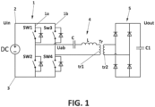
- LLC Series Resonant Converter topology (LLC-SRC) as the one shown in Figure 1 .
- This topology of converters belong to the so-called family of resonant converters that takes advantage of the resonance between their passive components to have soft-switching and, therefore, reduce the switching losses. Thanks to this reduction of losses, it allows increasing the efficiency of the converter and increase the switching frequency to reduce the size of the converter.
- Resonant converters are usually controlled by means of the frequency variation.
- the control tends to startup the converter with 0V at the output by switching at the highest frequency and 50% duty-cycle, and when the output voltage reaches the target voltage, the frequency is reduced to reach the output power demand.
- Some applications require high-power converters with fast output dynamics (e.g. precharging from 0V to 500V in less than 100 - 200ms). In turn, this implies reducing the output capacitors of the converter (e.g. 9 - 12uF for a 10 - 20kW equipment, instead of bulky aluminum capacitors of hundreds or thousands of uF).
- the only load of the converter are the discharge resistors (e.g. 100 - 200kOhm resistors), so that, there is a very small power consumption, less than 1W load in a 10 - 20kW converter.
- some applications require precharging (or voltage control) methods with high voltage accuracy/resolution (e.g. precharge setpoint with ⁇ 10V error in a 150 to 500V range). This is difficult to be obtained with the traditional approaches due to the aforementioned voltage increase worsen by the light load conditions. Therefore, it is necessary to start with a low duty-cycle, otherwise the voltage would increase too much at low voltages; and more discretization (e.g. with the burst mode) to cover a high output voltage range with enough accuracy/resolution.
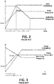
- a classical approach to solve this issue is a soft-start method with 2 stages, as the one shown in Figure 2 , wherein a first stage with variable duty-cycle and fixed frequency is performed, until a target voltage is reached, and a second stage with fixed duty-cycle and variable frequency.
- the first stage with small power pulses delivered to the resonant tank can be done by varying the pulse width, so the duty-cycle, or varying the phase-shift between branches (in case of more than 1 branch) and maintaining the duty-cycle at 50%.
- Patent publication US-20150280545 A1 describes a solution that takes advantage of using simpler controllers, and propose a method of start-up based on varying duty-cycle and frequency at the same time (see Figure 3 ) starting from minimum duty-cycle and maximum frequency (the change in duty-cycle and frequency is based on 1 switch (top or bottom) or 2 switches; and it depends on a ramp or an exponential curve, starting from minimum duty and maximum frequency.
- the maximum frequency of operation can get close to the resonance frequency, so even if this frequency is taken to the maximum it is not enough to avoid overcurrents, as the prior art using initial frequency at least is between 1.5 and 3 times the resonance frequency.
- the invention is defined in the attached independent claim, and satisfactorily solves the above-mentioned drawbacks of the prior art, by providing a method of soft-start and output voltage control that comprises two stages, namely: a first stage or rising time wherein the output voltage is slowly increased until an output target voltage is reached, and subsequently a second stage or holding time during which the resonant converter output voltage is controlled to maintain it at the desired value.
- the invention also refers to a DC-DC resonant converter system, comprising at least one resonant converter adapted to operate in accordance with the above-described method.
- the system comprises a plurality of resonant converters connected in series and/or in parallel.
- the resonant converter comprises: an input stage including a switch network with semiconductor switching devices for converting a DC input voltage into an AC voltage, a resonant tank or circuit connected at the output of the switch network which receives the AC voltage, and a converter controller for controlling switching of the semiconductor switching devices of the switch network.
- the controller is adapted to operate the semiconductors switching devices during a start up process of the resonant converter, such that the switching frequency and the duty-cycle are kept constant during a first time interval (t1). Keeping switching frequency and duty-cycle constant during a first time interval (t1), prevent overcurrents at the first stage of the starting process, right when the capacitor is more discharged is when current rises, so the system hold for a certain time to stabilize the current or the slope of the current growth before turning to the next interval (t2).
- the first time interval (t1) starts in the instant when the converter is started.
- the duration of the first time interval (t1) can be determined based on one of the following criteria:
- the term semiconductor switching device refers to a variety of transistors or other power switching devices as known in the state of art (i.e: IGBT, MOSFET, etc), built in any kind of semiconductor technology (Si, SiC, GaN and or other wide-bandgap devices) but not limited to it, that alone, in combination or with partial utilization behave as a current bidirectional two-quadrant switching devices.
- the controller is adapted to operate the converter during said first time interval (t1) such that the switching frequency is maximum and duty-cycle is minimum, wherein the maximum frequency and minimum duty-cycle are determined by the capacity of the circuit components like: microcontroller, drivers, and power semiconductors switching devices.
- maximum switching frequency and minimum or maximum duty-cycle belong to the common general knowledge of a skilled person in the art, as it is known that the maximum switching frequency and minimum duty-cycle are determined by the capacity of the hardware, that is, by the components implementing each particular application, like: the microcontroller, drivers, and power semiconductors switching devices.
- the controller is further adapted to operate the converter during a second time interval (t2) consecutive to the first time interval (t1) during the start up process, in a way that the switching frequency is progressively decreased and the duty-cycle is progressively increased.
- the duty-cycle is progressively increased during the second time interval (t2) up to a maximum that is up to about 50% or below the maximum.
- the second time interval (t2) terminates when the duty-cycle reaches its maximum.
- the second time interval (t2) is within the range 5ms - 200ms, and more preferably within the range 10ms - 100ms.
- the controller is further adapted to operate the converter during a third time interval (t3) once the duty-cycle has reached its maximum value, during which the switching frequency is progressively decreased (until a value dependent on the requested voltage and power), and the duty-cycle is kept constant (at its maximum value).
- This third time interval (t3) is consecutive to the second time interval (t2), and it lasts until a setpoint of the converter output voltage (Uout) is reached.
- the third time interval (t3) is within the range 20ms - 500ms, and more preferably within the range 50ms - 200ms.
- the controller is further adapted such that when an output target voltage has been reached (end of third time interval (t3)), the resonant converter is operated in a burst mode to maintain a desired output target voltage during the rest of operation of the resonant converter.
- the controller is further adapted to operate the resonant converter in a burst mode during at least one of the: first, second or third time intervals.
- the controller is further adapted to operate the switch network to set drive pulses of the semiconductor switching devices to perform a Zero Voltage Switching (ZVS) operation of the network switch.
- ZVS Zero Voltage Switching
- an output stage is provided which can embodied as any kind of converter or rectifier either based on diode rectification or with synchronous rectification, to provide an output DC voltage of the resonant converter.
- This output stage or rectifier is coupled to the resonant circuit directly or by means of an isolation transformer.
- a transformer is used for coupling the output stage or rectifier to the resonant tank, such that a primary winding of the transformer is coupled to the resonant tank, that is, the primary winding is part of the resonant tank, and the output stage or rectifier is connected to a secondary winding of the transformer.
- the switch network can be embodied as a half bridge circuit, or as a full bridge circuit as the one shown in Figure 1 , including one, two or more branches.
- the switch network comprises at least one branch including two semiconductor switching devices connected in series between two input terminals of the switch network, and the controller is preferably adapted to maintain the two semiconductor switching devices switched-off during a dead time, which extends in between two consecutive semi-pulses generated by the switch network.
- the dead time is a predetermined period time, and it is the minimum time that the switches have to be switched-off to avoid cross-conduction (the simultaneous turn-on of the switches of the same branch).
- the converter controller comprises a digital microcontroller.
- Another aspect of the invention refers to a method for controlling a resonant converter, wherein the resonant converter preferably comprises an input stage including a switch network for converting a DC input voltage into an AC voltage, a resonant tank connected at the output of the switch network, and a converter controller for controlling switching of the semiconductor switching devices of the switch network, and an output stage or rectifier coupled to the resonant tank.
- the resonant converter preferably comprises an input stage including a switch network for converting a DC input voltage into an AC voltage, a resonant tank connected at the output of the switch network, and a converter controller for controlling switching of the semiconductor switching devices of the switch network, and an output stage or rectifier coupled to the resonant tank.
- the resonant converter is started up by keeping the switching frequency and the duty-cycle constant during a first time interval (t1).
- the resonant converter is operated such that during this first time interval (t1), the switching frequency is maximum and the duty-cycle is minimum.
- the duration of the first time interval (t1) is the same as the one defined above for the converter of the invention.
- the method of the invention is preferably implemented in a resonant converter comprising: a switch network including semiconductor switching devices for converting a DC input voltage into an AC voltage, a resonant circuit connected at the output of the switch network which receives the AC voltage, and a converter controller for controlling switching of the semiconductor switching devices.
- the switch network is operated in a burst mode during the starting up process, which allows starting with a very low duty-cycle and high frequency (very low power and so inrush current) with the advantage of avoiding sudden increases of voltage with a better discretization and accuracy.
- a burst mode is also applied during a holding interval to maintain a desired output target voltage at the output of the resonant converter.
- the burst mode in both the method and the converter of the invention can be carried out either with constant ON and OFF times, or with variable ON and OFF times, for example dependant on algorithms.
- the resonant converter and the control method according to the invention combining: burst mode, duty-cycle and frequency variation as described above, achieves a more precise and discrete control of the power delivered to the output and, thus, limits inrush currents, fast voltage slopes and high voltage ripples.
- the resonant converter and the control method provide more output voltage and power accuracy at start up process even with during light load conditions.
- the switching frequency and duty-cycle can be varied as a lineal function as a ramp up or down, or alternatively they can be varied as a curve, or as any algorithm.
- the duty-cycle starts at its minimum and the frequency at its maximum, but they may be started at another point as well as finishing in other intermediates.
- the duty-cycle control can be done only by modifying the pulse width.
- the duty-cycle control can be done by varying the phase-shift between branches and maintaining the duty-cycle at 50%.
- the phase-shift control can be extended to other switch network topologies having more than two branches.
- Using a burst mode operation both during the start up process and the holding interval provides a more precise control of the output voltage, and avoids voltage overshoots and higher output voltage ripples in very light load conditions.
- the invention provides a precise soft-start and output voltage control method for resonant converters in general, but especially adapted for applications that require very wide load conditions (e.g. high voltage and current/power range from 150V - 800V and 0,5A - 70A).
- the switching frequency could be below 100kHz when trying to supply 800V and 30A (high voltage and current/power), but the switching frequency could be above 300kHz when trying to deliver to the load 150V and 0,5A (lower voltage and current/power), thus, the resonant frequency of the circuit should be chosen high (e.g. 320 kHz) to allow giving this low power at low voltage.
- the present invention is especially advantageous when used as a precharge / soft-start method with a lower duty-cycle at the beginning, an especial switching pattern and a burst method, without the use of a specific precharge circuit.
- the present invention provides a fast and precise soft-start and output voltage control method specially adapted for light load conditions (e.g. allows controlling the voltage for powers up to 0.003% of nominal power), which is especially advantageous for those applications that require high-power converters with fast output dynamics (e.g. precharging from 0V to 800V in less than 100-200ms).
- this implies a reduction of the size of output capacitors of the converter (e.g. 5 - 20uF for a 10 - 20kW equipment, the most used technology is based on MKP capacitors, instead of bulky aluminum capacitors of hundreds or thousands of uF).
- the present invention provides a precise soft-start method as described above, with a switching pattern that reduces the semiconductors stress, which is especially beneficial for systems with wide output load conditions and also with low fmaximum / fresonant ratio) to avoid high frequency requirements at low power.
- the precise soft-start method of the invention eliminates the need of additional precharge system (e.g. relay + precharge resistors + control) between the converter and the load.
- additional precharge system e.g. relay + precharge resistors + control
- the traditional systems have a power relay with current limiting resistors between the OBC and the battery, which is used to precharge the OBC's output capacitors when starts the charge of the battery.
- the invention can be particularly applied for automotive field applications, but it can also be applied to any power supply unit or power-converter device that includes a DC to DC converter.
- Figure 1 shows an exemplary implementation of a LLC-SRC resonant converter according to the invention, wherein the input stage is a switch network as a full bridge circuit, and the output stage is a bridge diode rectifier.
- the switch network can be embodied as a half bridge circuit, or any other typology with more than two branches
- the output stage can be embodied as any kind of output stage or rectifier either based on diode rectification or with synchronous rectification, to provide an output DC voltage of the resonant converter.
- This output stage or rectifier is coupled to the resonant circuit directly or by means of an isolation transformer.
- the resonant converter shown therein comprises a full-bridge circuit (1), as switch network, including a first branch (1a) having first and second semiconductor switching devices (SW1,SW2) connected in series, and second branch (1b) including a third and fourth semiconductor switching devices (SW3,SW4) connected in series, wherein the first and second branches (1a,1b) are connected in parallel with respect to each other between two input terminals (2,3) of the converter, such that a DC input voltage (Uin) connected at the input terminals (2,3) is converted in a known manner in an AC voltage at the output (Uab) of the full-bridge circuit (1).
- a DC input voltage (Uin) connected at the input terminals (2,3) is converted in a known manner in an AC voltage at the output (Uab) of the full-bridge circuit (1).
- the resonant converter further comprises a resonant circuit (4) having a capacitor (C) and an inductor (L) connected in series at the output (Uab) of the full-bridge circuit (1).
- the output (Uab) is taken at the two center connections between the semiconductor switching devices of each branch.
- the resonant converter includes an isolation transformer (Tr) coupled at the output (Uab) of the switch network (1), such that a primary winding (tr1) of the transformer is coupled in series with the capacitor (C) and inductor (L), so that this primary winding (tr1) is also part of the resonant tank (4).
- Tr isolation transformer
- the output stage is a full bridge diode rectifier (5) connected to the secondary winding (tr2) of the transformer (Tr), followed by an output capacitor (C1) to smooth the DC output voltage (Uout) (5).
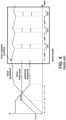
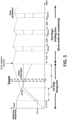
- the converter controller (not shown) for controlling switching of the semiconductor switching devices (SW1-SW4), is preferably implemented as a digital microcontroller, and it is adapted, that is, it is programmed to implement the control method of the invention, as represented in Figure 5 .
- the invention provides a control method of soft-start and output voltage control for resonant converters, wherein the converter is operated as to perform two main sequential stages as shown in Figure 5 :
- This starting up process involves three sequential time intervals (t1 ⁇ t3):
- the second time interval (t2) is shorter than the third time interval (t3) to reach quickly a situation where the control of the converter depends only on the switching frequency.
- the switching technique used during time intervals (t1 ⁇ t2) is based on switching the two complementary switches of the two branches (1a, 1b), for example (SW1,SW4) and (SW2,SW3) in the switch network of Figure 1 , to set drive semi-pulses of the semiconductor switching devices in such a way that Zero Voltage Switching (ZVS) of the switch network is guaranteed and surge current is low.
- ZVS Zero Voltage Switching
- first semi pulse complementary switches SW1,SW4 are switched ON and the other switches (SW2, SW3) remain in OFF state.
- switches SW1,SW4 are switched OFF maintaining switches (SW2, SW3) OFF, such that all switches are kept OFF for a first dead time.
- switches (SW2,SW3) are switched OFF, while switches (SW1,SW4) are kept OFF, such that all switches are again kept OFF for a second dead time.
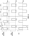
- the duration of the dead time is constant, whereas the OFF time is constant during first and third time intervals t1, t3.
- the OFF time might be lower, equal or greater than the dead time.
- the OFF time is greater than the dead time during the first time interval (t1).
- second time interval (t2) the OFF time is zero when the maximum duty-cycle of the system has been reached, that is, when there is only dead time between semi-pulses.
- the OFF-time is zero in time period (t3), when the maximum duty-cycle (Dmax) of the system has been reached, if the duty-cycle is lower than the maximum, then the OFF time should be more than 0.
- the dead time is the minimum time that the switches have to be switched-off to avoid short circuits between switches of the same branch.
- semiconductor switches of Si require a deadtime below of 200ns, better between 150 to 200ns; for SiC below of 150ns, better between 50 to 150ns; and for GaN below 150ns, better between 20 to 150ns, for a switching frequency within the range 100Khz ⁇ 1MHz.
- This above-described switching technique increases the (Uab) maximum frequency (1/T ab ) while maintaining a 50% duty-cycle signal or to a predefined value below the maximum, and thus guarantee ZVS and reduce surge currents.
- this switching technique allows: a reduction of surge current during start-up, ZVS during this dead and/or OFF times and a voltage and power accuracy improvement at light load conditions.
- the controller is further adapted to operate the switch network in a burst mode during at least one of the: first, second or third time intervals (t1, t2 and t3).
- a burst mode operation is performed during the entire first stage of rising time.
- Ton and Toff periods are applied while the duty-cycle and switching frequency is constant or modified, as represented in Figure 7 , which allows starting with a very low duty-cycle and highest frequency (very low power and so inrush current) with the advantage of avoiding sudden increases of voltage with a better discretization and accuracy.
- This second stage starts once the output target voltage (Uout) has been reached (end of third time interval t3), and it is maintained with a hysteresis by turning ON and OFF the switch network, like a second and bigger burst mode.
- a given threshold target voltage minus a delta of voltage
- the burst mode operation is activated again; and when the target voltage is reached again, or when the target voltage is exceeded by a certain value, then the burst mode operation is discontinued.
- the burst mode operation is kept, as represented in Figure 5 , which allows controlling the output voltage (Uout) more precisely, avoiding voltage overshoots and higher output voltage ripples in very light load conditions.
Landscapes
- Engineering & Computer Science (AREA)
- Power Engineering (AREA)
- Dc-Dc Converters (AREA)
Priority Applications (2)
| Application Number | Priority Date | Filing Date | Title |
|---|---|---|---|
| EP21382739.7A EP4131758A1 (fr) | 2021-08-05 | 2021-08-05 | Système de convertisseur résonant avec démarrage en douceur et commande de tension de sortie et son procédé de commande |
| CN202210920510.5A CN115706536A (zh) | 2021-08-05 | 2022-08-02 | 带软启动和输出电压控制的谐振转换器系统及其控制方法 |
Applications Claiming Priority (1)
| Application Number | Priority Date | Filing Date | Title |
|---|---|---|---|
| EP21382739.7A EP4131758A1 (fr) | 2021-08-05 | 2021-08-05 | Système de convertisseur résonant avec démarrage en douceur et commande de tension de sortie et son procédé de commande |
Publications (1)
| Publication Number | Publication Date |
|---|---|
| EP4131758A1 true EP4131758A1 (fr) | 2023-02-08 |
Family
ID=77265040
Family Applications (1)
| Application Number | Title | Priority Date | Filing Date |
|---|---|---|---|
| EP21382739.7A Pending EP4131758A1 (fr) | 2021-08-05 | 2021-08-05 | Système de convertisseur résonant avec démarrage en douceur et commande de tension de sortie et son procédé de commande |
Country Status (2)
| Country | Link |
|---|---|
| EP (1) | EP4131758A1 (fr) |
| CN (1) | CN115706536A (fr) |
Cited By (1)
| Publication number | Priority date | Publication date | Assignee | Title |
|---|---|---|---|---|
| WO2024234389A1 (fr) * | 2023-05-18 | 2024-11-21 | Stmicroelectronics (China) Investment Co., Ltd | Procédé de commande de démarrage progressif pour convertisseur résonant llc entrelacé triphasé |
Families Citing this family (2)
| Publication number | Priority date | Publication date | Assignee | Title |
|---|---|---|---|---|
| CN119727354A (zh) * | 2025-02-27 | 2025-03-28 | 西安图为电气技术有限公司 | 双向dc/dc变换器软启动方法、装置及计算机设备 |
| CN121485208B (zh) * | 2026-01-07 | 2026-04-21 | 潍柴动力股份有限公司 | 一种预充电路的诊断方法、设备及介质 |
Citations (6)
| Publication number | Priority date | Publication date | Assignee | Title |
|---|---|---|---|---|
| JP2009189108A (ja) * | 2008-02-05 | 2009-08-20 | Shindengen Electric Mfg Co Ltd | スイッチング電源 |
| US8018740B2 (en) | 2010-01-07 | 2011-09-13 | Texas Instruments Incorporated | LLC soft start by operation mode switching |
| WO2014074923A1 (fr) * | 2012-11-09 | 2014-05-15 | Murata Manufacturing Co., Ltd. | Mise sous tension sans appel de courant pour convertisseurs auto-oscillants |
| US20160181927A1 (en) | 2014-12-18 | 2016-06-23 | Infineon Technologies Austria Ag | System and Method for a Switched-Mode Power Supply |
| US9893609B1 (en) | 2014-05-28 | 2018-02-13 | Bel Power Solutions Inc. | Method to operate a resonant converter at a characteristic frequency of the power stage |
| CN112271918A (zh) * | 2020-09-16 | 2021-01-26 | 浙江吉利控股集团有限公司 | 一种用于车载电源充电的软启动方法及系统 |
-
2021
- 2021-08-05 EP EP21382739.7A patent/EP4131758A1/fr active Pending
-
2022
- 2022-08-02 CN CN202210920510.5A patent/CN115706536A/zh active Pending
Patent Citations (7)
| Publication number | Priority date | Publication date | Assignee | Title |
|---|---|---|---|---|
| JP2009189108A (ja) * | 2008-02-05 | 2009-08-20 | Shindengen Electric Mfg Co Ltd | スイッチング電源 |
| US8018740B2 (en) | 2010-01-07 | 2011-09-13 | Texas Instruments Incorporated | LLC soft start by operation mode switching |
| WO2014074923A1 (fr) * | 2012-11-09 | 2014-05-15 | Murata Manufacturing Co., Ltd. | Mise sous tension sans appel de courant pour convertisseurs auto-oscillants |
| US20150280545A1 (en) | 2012-11-09 | 2015-10-01 | Murata Manufacturing Co., Ltd. | Soft-start for resonant converters |
| US9893609B1 (en) | 2014-05-28 | 2018-02-13 | Bel Power Solutions Inc. | Method to operate a resonant converter at a characteristic frequency of the power stage |
| US20160181927A1 (en) | 2014-12-18 | 2016-06-23 | Infineon Technologies Austria Ag | System and Method for a Switched-Mode Power Supply |
| CN112271918A (zh) * | 2020-09-16 | 2021-01-26 | 浙江吉利控股集团有限公司 | 一种用于车载电源充电的软启动方法及系统 |
Non-Patent Citations (1)
| Title |
|---|
| YU TANG ET AL: "Research on Open-loop Soft-start Strategy of CLLLC Bi-directional Resonant Converter", 2018 IEEE INTERNATIONAL POWER ELECTRONICS AND APPLICATION CONFERENCE AND EXPOSITION (PEAC), IEEE, 4 November 2018 (2018-11-04), pages 1 - 6, XP033477102, DOI: 10.1109/PEAC.2018.8590641 * |
Cited By (1)
| Publication number | Priority date | Publication date | Assignee | Title |
|---|---|---|---|---|
| WO2024234389A1 (fr) * | 2023-05-18 | 2024-11-21 | Stmicroelectronics (China) Investment Co., Ltd | Procédé de commande de démarrage progressif pour convertisseur résonant llc entrelacé triphasé |
Also Published As
| Publication number | Publication date |
|---|---|
| CN115706536A (zh) | 2023-02-17 |
Similar Documents
| Publication | Publication Date | Title |
|---|---|---|
| EP3198710B1 (fr) | Procédé de commande pour des convertisseurs de puissance abaisseurs-élévateurs de tension | |
| US10658934B2 (en) | Quasi-resonant converter with efficient light-load operation and method therefor | |
| CN103296892B (zh) | 谐振变换器的多模工作和控制 | |
| US6618274B2 (en) | Synchronous rectifier controller to eliminate reverse current flow in a DC/DC converter output | |
| US9712045B2 (en) | System and method for a startup cell circuit | |
| JP4824524B2 (ja) | 単方向dc−dcコンバータおよびその制御方法 | |
| US7852640B2 (en) | System and method for providing control for switch-mode power supply | |
| US8149597B2 (en) | Intermediate bus architecture with a quasi-regulated bus converter | |
| US20070013349A1 (en) | Zero voltage switching buck converter | |
| US7272021B2 (en) | Power converter with isolated and regulated stages | |
| EP4131758A1 (fr) | Système de convertisseur résonant avec démarrage en douceur et commande de tension de sortie et son procédé de commande | |
| US11757365B2 (en) | Dynamic transient control in resonant converters | |
| TWI790657B (zh) | 控制切換模式電源中的反向電流以實現零電壓切換 | |
| CN114499194B (zh) | 电源控制装置 | |
| JP6012822B1 (ja) | 電力変換装置 | |
| US8503195B1 (en) | System and method for zero volt switching of half bridge converters during startup and short circuit conditions | |
| US20050057951A1 (en) | Controlled synchronous rectifier for controlling an output voltage of a switched mode power supply | |
| GB2524065A (en) | Converter | |
| JP2022050131A (ja) | 電力変換装置、電力変換装置の制御方法、及び電力システム | |
| JP2024097584A (ja) | 電流共振型dc/dcコンバータ | |
| CN114567149A (zh) | 电力转换器控制器、电力转换器及操作电力转换器的方法 | |
| US20260095091A1 (en) | Hybrid Power Converter Circuit With Resonant Mode and Pulse Width Modulation Mode | |
| EP4507176A1 (fr) | Contrôleur et procédé de commande pour mode rafale dans des convertisseurs llc | |
| CN116264435B (zh) | 具有软进入与软脱出的电源控制器以及控制方法 | |
| JP2010057207A (ja) | スイッチング電源装置 |
Legal Events
| Date | Code | Title | Description |
|---|---|---|---|
| PUAI | Public reference made under article 153(3) epc to a published international application that has entered the european phase |
Free format text: ORIGINAL CODE: 0009012 |
|
| STAA | Information on the status of an ep patent application or granted ep patent |
Free format text: STATUS: THE APPLICATION HAS BEEN PUBLISHED |
|
| AK | Designated contracting states |
Kind code of ref document: A1 Designated state(s): AL AT BE BG CH CY CZ DE DK EE ES FI FR GB GR HR HU IE IS IT LI LT LU LV MC MK MT NL NO PL PT RO RS SE SI SK SM TR |
|
| STAA | Information on the status of an ep patent application or granted ep patent |
Free format text: STATUS: REQUEST FOR EXAMINATION WAS MADE |
|
| 17P | Request for examination filed |
Effective date: 20230802 |
|
| RBV | Designated contracting states (corrected) |
Designated state(s): AL AT BE BG CH CY CZ DE DK EE ES FI FR GB GR HR HU IE IS IT LI LT LU LV MC MK MT NL NO PL PT RO RS SE SI SK SM TR |
|
| STAA | Information on the status of an ep patent application or granted ep patent |
Free format text: STATUS: EXAMINATION IS IN PROGRESS |
|
| 17Q | First examination report despatched |
Effective date: 20240723 |
|
| RAP1 | Party data changed (applicant data changed or rights of an application transferred) |
Owner name: FICOSA AUTOMOTIVE, S.L.U. |