EP4131761A1 - Circuit de commande de conversion résonnante cc-cc non isolée, et procédé de commande - Google Patents
Circuit de commande de conversion résonnante cc-cc non isolée, et procédé de commande Download PDFInfo
- Publication number
- EP4131761A1 EP4131761A1 EP21797135.7A EP21797135A EP4131761A1 EP 4131761 A1 EP4131761 A1 EP 4131761A1 EP 21797135 A EP21797135 A EP 21797135A EP 4131761 A1 EP4131761 A1 EP 4131761A1
- Authority
- EP
- European Patent Office
- Prior art keywords
- switching transistor
- output interface
- voltage
- phase shift
- shift angle
- Prior art date
- Legal status (The legal status is an assumption and is not a legal conclusion. Google has not performed a legal analysis and makes no representation as to the accuracy of the status listed.)
- Granted
Links
Images






Classifications
-
- H—ELECTRICITY
- H02—GENERATION; CONVERSION OR DISTRIBUTION OF ELECTRIC POWER
- H02M—APPARATUS FOR CONVERSION BETWEEN AC AND AC, BETWEEN AC AND DC, OR BETWEEN DC AND DC, AND FOR USE WITH MAINS OR SIMILAR POWER SUPPLY SYSTEMS; CONVERSION OF DC OR AC INPUT POWER INTO SURGE OUTPUT POWER; CONTROL OR REGULATION THEREOF
- H02M3/00—Conversion of DC power input into DC power output
- H02M3/02—Conversion of DC power input into DC power output without intermediate conversion into AC
- H02M3/04—Conversion of DC power input into DC power output without intermediate conversion into AC by static converters
- H02M3/10—Conversion of DC power input into DC power output without intermediate conversion into AC by static converters using discharge tubes with control electrode or semiconductor devices with control electrode
- H02M3/145—Conversion of DC power input into DC power output without intermediate conversion into AC by static converters using discharge tubes with control electrode or semiconductor devices with control electrode using devices of a triode or transistor type requiring continuous application of a control signal
- H02M3/155—Conversion of DC power input into DC power output without intermediate conversion into AC by static converters using discharge tubes with control electrode or semiconductor devices with control electrode using devices of a triode or transistor type requiring continuous application of a control signal using semiconductor devices only
- H02M3/156—Conversion of DC power input into DC power output without intermediate conversion into AC by static converters using discharge tubes with control electrode or semiconductor devices with control electrode using devices of a triode or transistor type requiring continuous application of a control signal using semiconductor devices only with automatic control of output voltage or current, e.g. switching regulators
- H02M3/158—Conversion of DC power input into DC power output without intermediate conversion into AC by static converters using discharge tubes with control electrode or semiconductor devices with control electrode using devices of a triode or transistor type requiring continuous application of a control signal using semiconductor devices only with automatic control of output voltage or current, e.g. switching regulators including plural semiconductor devices as final control devices for a single load
-
- H—ELECTRICITY
- H02—GENERATION; CONVERSION OR DISTRIBUTION OF ELECTRIC POWER
- H02M—APPARATUS FOR CONVERSION BETWEEN AC AND AC, BETWEEN AC AND DC, OR BETWEEN DC AND DC, AND FOR USE WITH MAINS OR SIMILAR POWER SUPPLY SYSTEMS; CONVERSION OF DC OR AC INPUT POWER INTO SURGE OUTPUT POWER; CONTROL OR REGULATION THEREOF
- H02M3/00—Conversion of DC power input into DC power output
- H02M3/01—Resonant DC/DC converters
-
- H—ELECTRICITY
- H02—GENERATION; CONVERSION OR DISTRIBUTION OF ELECTRIC POWER
- H02M—APPARATUS FOR CONVERSION BETWEEN AC AND AC, BETWEEN AC AND DC, OR BETWEEN DC AND DC, AND FOR USE WITH MAINS OR SIMILAR POWER SUPPLY SYSTEMS; CONVERSION OF DC OR AC INPUT POWER INTO SURGE OUTPUT POWER; CONTROL OR REGULATION THEREOF
- H02M1/00—Details of apparatus for conversion
- H02M1/0048—Circuits or arrangements for reducing losses
- H02M1/0054—Transistor switching losses
- H02M1/0058—Transistor switching losses by employing soft switching techniques, i.e. commutation of transistors when applied voltage is zero or when current flow is zero
-
- H—ELECTRICITY
- H02—GENERATION; CONVERSION OR DISTRIBUTION OF ELECTRIC POWER
- H02M—APPARATUS FOR CONVERSION BETWEEN AC AND AC, BETWEEN AC AND DC, OR BETWEEN DC AND DC, AND FOR USE WITH MAINS OR SIMILAR POWER SUPPLY SYSTEMS; CONVERSION OF DC OR AC INPUT POWER INTO SURGE OUTPUT POWER; CONTROL OR REGULATION THEREOF
- H02M3/00—Conversion of DC power input into DC power output
- H02M3/02—Conversion of DC power input into DC power output without intermediate conversion into AC
- H02M3/04—Conversion of DC power input into DC power output without intermediate conversion into AC by static converters
- H02M3/10—Conversion of DC power input into DC power output without intermediate conversion into AC by static converters using discharge tubes with control electrode or semiconductor devices with control electrode
- H02M3/145—Conversion of DC power input into DC power output without intermediate conversion into AC by static converters using discharge tubes with control electrode or semiconductor devices with control electrode using devices of a triode or transistor type requiring continuous application of a control signal
- H02M3/155—Conversion of DC power input into DC power output without intermediate conversion into AC by static converters using discharge tubes with control electrode or semiconductor devices with control electrode using devices of a triode or transistor type requiring continuous application of a control signal using semiconductor devices only
- H02M3/156—Conversion of DC power input into DC power output without intermediate conversion into AC by static converters using discharge tubes with control electrode or semiconductor devices with control electrode using devices of a triode or transistor type requiring continuous application of a control signal using semiconductor devices only with automatic control of output voltage or current, e.g. switching regulators
- H02M3/158—Conversion of DC power input into DC power output without intermediate conversion into AC by static converters using discharge tubes with control electrode or semiconductor devices with control electrode using devices of a triode or transistor type requiring continuous application of a control signal using semiconductor devices only with automatic control of output voltage or current, e.g. switching regulators including plural semiconductor devices as final control devices for a single load
- H02M3/1582—Buck-boost converters
-
- H—ELECTRICITY
- H02—GENERATION; CONVERSION OR DISTRIBUTION OF ELECTRIC POWER
- H02M—APPARATUS FOR CONVERSION BETWEEN AC AND AC, BETWEEN AC AND DC, OR BETWEEN DC AND DC, AND FOR USE WITH MAINS OR SIMILAR POWER SUPPLY SYSTEMS; CONVERSION OF DC OR AC INPUT POWER INTO SURGE OUTPUT POWER; CONTROL OR REGULATION THEREOF
- H02M1/00—Details of apparatus for conversion
- H02M1/0083—Converters characterised by their input or output configuration
-
- H—ELECTRICITY
- H02—GENERATION; CONVERSION OR DISTRIBUTION OF ELECTRIC POWER
- H02M—APPARATUS FOR CONVERSION BETWEEN AC AND AC, BETWEEN AC AND DC, OR BETWEEN DC AND DC, AND FOR USE WITH MAINS OR SIMILAR POWER SUPPLY SYSTEMS; CONVERSION OF DC OR AC INPUT POWER INTO SURGE OUTPUT POWER; CONTROL OR REGULATION THEREOF
- H02M3/00—Conversion of DC power input into DC power output
- H02M3/02—Conversion of DC power input into DC power output without intermediate conversion into AC
- H02M3/04—Conversion of DC power input into DC power output without intermediate conversion into AC by static converters
- H02M3/06—Conversion of DC power input into DC power output without intermediate conversion into AC by static converters using resistors or capacitors, e.g. potential divider
- H02M3/07—Conversion of DC power input into DC power output without intermediate conversion into AC by static converters using resistors or capacitors, e.g. potential divider using capacitors charged and discharged alternately by semiconductor devices with control electrode, e.g. charge pumps
-
- H—ELECTRICITY
- H02—GENERATION; CONVERSION OR DISTRIBUTION OF ELECTRIC POWER
- H02M—APPARATUS FOR CONVERSION BETWEEN AC AND AC, BETWEEN AC AND DC, OR BETWEEN DC AND DC, AND FOR USE WITH MAINS OR SIMILAR POWER SUPPLY SYSTEMS; CONVERSION OF DC OR AC INPUT POWER INTO SURGE OUTPUT POWER; CONTROL OR REGULATION THEREOF
- H02M3/00—Conversion of DC power input into DC power output
- H02M3/02—Conversion of DC power input into DC power output without intermediate conversion into AC
- H02M3/04—Conversion of DC power input into DC power output without intermediate conversion into AC by static converters
- H02M3/06—Conversion of DC power input into DC power output without intermediate conversion into AC by static converters using resistors or capacitors, e.g. potential divider
- H02M3/07—Conversion of DC power input into DC power output without intermediate conversion into AC by static converters using resistors or capacitors, e.g. potential divider using capacitors charged and discharged alternately by semiconductor devices with control electrode, e.g. charge pumps
- H02M3/072—Conversion of DC power input into DC power output without intermediate conversion into AC by static converters using resistors or capacitors, e.g. potential divider using capacitors charged and discharged alternately by semiconductor devices with control electrode, e.g. charge pumps adapted to generate an output voltage whose value is lower than the input voltage
-
- Y—GENERAL TAGGING OF NEW TECHNOLOGICAL DEVELOPMENTS; GENERAL TAGGING OF CROSS-SECTIONAL TECHNOLOGIES SPANNING OVER SEVERAL SECTIONS OF THE IPC; TECHNICAL SUBJECTS COVERED BY FORMER USPC CROSS-REFERENCE ART COLLECTIONS [XRACs] AND DIGESTS
- Y02—TECHNOLOGIES OR APPLICATIONS FOR MITIGATION OR ADAPTATION AGAINST CLIMATE CHANGE
- Y02B—CLIMATE CHANGE MITIGATION TECHNOLOGIES RELATED TO BUILDINGS, e.g. HOUSING, HOUSE APPLIANCES OR RELATED END-USER APPLICATIONS
- Y02B70/00—Technologies for an efficient end-user side electric power management and consumption
- Y02B70/10—Technologies improving the efficiency by using switched-mode power supplies [SMPS], i.e. efficient power electronics conversion e.g. power factor correction or reduction of losses in power supplies or efficient standby modes
Definitions
- Embodiments of this application relate to the field of circuit technologies, and in particular, to a non-isolated DCDC resonant conversion control circuit and a control method.
- non-isolated DCDC buck-boost converter With the development of lithium battery applications, there are increasingly high demands for a non-isolated DCDC buck-boost converter.
- various topologies and technologies of non-isolated DCDC converters are proposed.
- a basic model based on Buck and Boost is basically used, and a current is generally a triangular wave. Content of high-order harmonic waves is high, and this is not conducive to further improvement of efficiency.
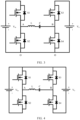
- FIG. 1 is a topology diagram of a circuit of an existing non-isolated DCDC buck-boost converter.
- FIG. 2 is a waveform diagram of a current in an inductor L in the circuit shown in FIG. 1 .
- the circuit includes a power supply Vin, a switch S1, a switch S2, a switch S3, a switch S4, an inductor L, and an output Vo.
- S1 is always on
- S2 is always off
- the inductor L and the switching transistors S2 and S3 implement a boost circuit function.
- the circuit When the circuit implements a buck function, S3 is always on, S4 is always off, and the inductor L and the switching transistors S1 and S2 implement a buck circuit function.
- the circuit is controlled in a conventional buck or boost critical continuous mode, so that a switching transistor can implement zero voltage switching (ZVS) on, but an inductance current is a triangular wave, a peak current is relatively large, and a turn-off current of the switching transistor is relatively large.
- ZVS zero voltage switching
- a waveform coefficient of the triangular wave is greater than a waveform coefficient of a sine wave, and has a larger conduction loss than the sine wave when same power is transmitted. High content of high-order harmonic waves in the triangular wave increases a high-order harmonic wave loss.
- Embodiments of this application provide a non-isolated DCDC resonant conversion control circuit and control method, to resolve a technical problem that a loss of an existing non-isolated DCDC buck-boost converter is large.
- a non-isolated DCDC resonant conversion control circuit in an embodiment of this application, and includes an input interface, a first switching transistor, a second switching transistor, a third switching transistor, a fourth switching transistor, an inductor, a capacitor, and an output interface. After being connected in series, the first switching transistor and the second switching transistor are coupled to the input interface in series. After being connected in series, the third switching transistor and the fourth switching transistor are coupled to the output interface in series. A node on which the first switching transistor and the second switching transistor are connected in series is an end A. A node on which the third switching transistor and the fourth switching transistor are connected in series is an end B.
- the inductor and the capacitor are coupled between the end A and the end B.
- a negative electrode of the input interface is coupled to a negative electrode of the output interface, or a positive electrode of the input interface is coupled to a positive electrode of the output interface.
- the inductor and the capacitor are connected in series, so that a current flowing through the inductor is a sine waveform.
- a waveform coefficient of a sine wave is small, and a conduction loss is low. Therefore, the circuit provided in this embodiment of this application can significantly reduce a circuit loss.
- the inductor and the capacitor are in a resonant working state.
- the second switching transistor when the first switching transistor is on, the second switching transistor is off; when the first switching transistor is off, the second switching transistor is on; when the third switching transistor is on, the fourth switching transistor is off; and when the third switching transistor is off, the fourth switching transistor is on.
- control circuit further includes a control unit; and the control unit is coupled to the first switching transistor, the second switching transistor, the third switching transistor, and the fourth switching transistor, and is configured to control on and off of the first switching transistor, the second switching transistor, the third switching transistor, and the fourth switching transistor.
- control circuit further includes a phase shift angle adjustment unit; and the phase shift angle adjustment unit is configured to determine the phase shift angle ⁇ of the voltage between the input interface and the output interface based on the voltage of the input interface and a target voltage of the output interface.
- control circuit further includes a frequency adjustment unit; and the frequency adjustment unit is configured to determine switching frequency of the first switching transistor in the control circuit based on the phase shift angle ⁇ and first target power or a first target current of the output interface.
- the frequency adjustment unit is further configured to adjust the switching frequency based on the phase shift angle ⁇ and second target power or a second target current of the output interface.
- a non-isolated DCDC resonant conversion control method is provided in an embodiment of this application. Based on the control circuit in the first aspect, the control method includes: determining a phase shift angle ⁇ of a voltage between an input interface and an output interface based on a voltage of the input interface and a target voltage of the output interface; determining switching frequency of a first switching transistor in the control circuit based on the phase shift angle ⁇ and first target power or a first target current of the output interface; and controlling, based on the phase shift angle ⁇ and the switching frequency, the first switching transistor, a second switching transistor, a third switching transistor, and a fourth switching transistor in the control circuit to be on or off.
- the determining the phase shift angle ⁇ based on the voltage of the input interface and the target voltage of the output interface by using a phase shift angle calculation formula includes: adjusting the phase shift angle ⁇ , and calculating a voltage of the output interface by using the phase shift angle calculation formula until the voltage of the output interface reaches the target voltage of the output interface.
- the method further includes: adjusting the switching frequency, and calculating power of the output interface by using the output power calculation formula until the power of the output interface reaches second target power of the output interface.
- the determining the switching frequency based on an output power calculation formula, the phase shift angle ⁇ , and the first target power or the first target current of the output interface includes: obtaining the target power of the output interface through calculation by using a target current of the output interface and the target voltage of the output interface; and determining the switching frequency based on the output power calculation formula, the phase shift angle ⁇ , and the first target power or the first target current of the output interface.
- the controlling, based on the phase shift angle ⁇ and the switching frequency, the first switching transistor, a second switching transistor, a third switching transistor, and a fourth switching transistor in the control circuit to be on or off specifically includes: when the first switching transistor is controlled to be on, controlling the second switching transistor to be off; when the first switching transistor is controlled to be off, controlling the second switching transistor to be on; when the third switching transistor is controlled to be on, controlling the fourth switching transistor to be off; and when the third switching transistor is controlled to be off, controlling the fourth switching transistor to be on.
- a power supply system in an embodiment of this application, and includes a power supply module and the DCDC resonant conversion control circuit according to the first aspect.
- the power supply module is connected to an input interface of the DCDC resonant conversion control circuit, and outputs electric energy to the DCDC resonant conversion control circuit, to increase an output voltage or decrease an output voltage.
- the power supply module is a lithium battery or a photovoltaic power supply.
- the inductor and the capacitor that are resonant are connected in series, so that a current flowing through the inductor is a sine waveform.
- a waveform coefficient of a sine wave is small, and a conduction loss is low. Therefore, the circuit provided in embodiments of this application can significantly reduce a circuit loss.
- the non-isolated DCDC resonant conversion control method provided in embodiments of this application not only the phase shift angle can be adjusted to enable the switching transistor to implement zero voltage switching ZVS on, but the switching frequency can also be adjusted. Therefore, ranges in which a voltage and power of the output interface can be adjusted are large, so that non-isolated wide-range DCDC resonant conversion is implemented.
- Embodiments of this application provide a non-isolated DCDC resonant conversion control circuit and control method, to resolve a technical problem that a loss of an existing non-isolated DCDC buck-boost converter is large.
- a word such as “example” or “for example” is used to represent giving an example, an illustration, or a description. Any embodiment or design solution described as “example” or “for example” in embodiments of this application should not be explained as being more preferred or advantageous over other embodiments or design solutions. Exactly, use of the word “example”, “for example” or the like is intended to present a relative concept in a specific manner.
- a waveform diagram of a current in an inductor L is shown in FIG. 2 and is a triangular wave, a peak current is large, and a turn-off current of a switching transistor is relatively large.
- a waveform coefficient of the triangular wave is greater than a waveform coefficient of a sine wave, and a conduction loss is also greater than that of the sine wave when same power is transmitted.
- High content of high-order harmonic waves of a triangular wave current increases a high-order harmonic wave loss.
- FIG. 3 is a circuit diagram 1 of a non-isolated DCDC resonant conversion control circuit according to an embodiment of this application.
- the circuit includes an input interface, an output interface, a switching transistor S1, a switching transistor S2, a switching transistor S3, a switching transistor S4, an inductor L, and a capacitor C.
- a voltage of the input interface is Vin.
- the input interface may be connected to a direct-current device, another power supply device (such as a lithium battery), another communication device, or the like. This is not limited in this embodiment of this application.
- a voltage of the output interface is Vo, and the output interface may also be connected to a direct-current device (such as a motor) or another communication device. This is not limited in this embodiment of this application.
- the switching transistor S1, the switching transistor S2, the switching transistor S3, and the switching transistor S4 may be switching transistors of a same type, or may be switching transistors of different types. This is not limited in this embodiment of this application.
- the switching transistor S1, the switching transistor S2, the switching transistor S3, and the switching transistor S4 may be transistors, may be MOS transistors, or may be insulated gate bipolar transistors (IGBT), and have controllable on and off functions. Specific types of the switching transistor S1, the switching transistor S2, the switching transistor S3, and the switching transistor S4 are not limited in this embodiment of this application.
- the switching transistor S1 and the switching transistor S2 are connected in series to form a front bridge arm.
- the front bridge arm is coupled to the input interface in series.
- the switching transistor S3 and the switching transistor S4 are connected in series to form a rear bridge arm.
- the rear bridge arm is coupled to the output interface in series.
- a midpoint at which the switching transistor S1 and the switching transistor S2 are connected in series is an end A.
- a midpoint at which the switching transistor S3 and the switching transistor S4 are connected in series is an end B.
- the inductor L and the capacitor C are connected in series between the end A and the end B.
- a negative electrode of the input interface is coupled to a negative electrode of the output interface
- the input interface and the output interface share a same negative electrode, and can provide a current loop.
- a positive electrode of the input interface is coupled to a positive electrode of the output interface
- the input interface and the output interface share a same positive electrode, and similarly, can provide a current loop.
- the inductor L and the capacitor C are coupled between the end A and the end B, as shown in FIG. 3 .
- the inductor L and the capacitor C are in a resonant working state.
- Resonance includes parallel resonance and serial resonance.
- serial resonance is described.
- a resonance circuit including the inductor L and the capacitor C that are connected in series is referred to as a series resonance circuit.
- XL is impedance of the inductor L
- XC is impedance of the capacitor C.
- ⁇ L 1 ⁇ C .
- ⁇ is angular frequency of a power supply of the series resonance circuit
- L is an inductance value of the inductor L
- C is a capacitance value of the capacitor C.
- a position of the inductor L and a position of the capacitor C may be exchanged.
- a circuit obtained after the exchange is similar to the circuit in the embodiment corresponding to FIG. 3 , and details are not described herein again.
- the capacitance value C selected in the circuit is relatively small, so that the inductor L and the capacitor C work in a resonant state.
- FIG. 4 is a circuit diagram 2 of a non-isolated DCDC resonant conversion control circuit according to an embodiment of this application.
- a negative electrode of an input interface in the circuit is not coupled to a negative electrode of an output interface, and a positive electrode of the input interface is coupled to a positive electrode of the output interface.
- This embodiment of this application may be applicable to a case in which an input device and an output device share a same positive electrode.
- an inductor L and a capacitor C are in a series resonant state.
- Another case of the circuit is similar to the embodiment corresponding to FIG. 3 , and details are not described herein again.
- FIG. 5 is a circuit diagram 3 of a non-isolated DCDC resonant conversion control circuit according to an embodiment of this application.
- a positive electrode and a negative electrode of an input interface in the circuit in FIG. 5 are opposite to those in the circuit shown in FIG. 3
- a positive electrode and a negative electrode of an output interface are also opposite to those in the circuit shown in FIG. 3 .
- the positive electrode of the input interface is coupled to the positive electrode of the output interface. Therefore, the embodiment corresponding to FIG. 5 may be applicable to a case in which an input device and an output device share a same positive electrode.
- Another case of the circuit is similar to the embodiment corresponding to FIG. 3 , and details are not described herein again.
- FIG. 6 is a circuit diagram 4 of a non-isolated DCDC resonant conversion control circuit according to an embodiment of this application.
- a position of an input interface in the circuit and a position of an output interface may be exchanged.
- the output interface is coupled to a switching transistor S 1 and a switching transistor S2 in series
- the input interface is coupled to a switching transistor S3 and a switching transistor S4 in series.
- the input interface may be connected to an input device such as a lithium battery, and the output interface may be connected to a direct-current device or the like.
- a proper device may be connected based on a requirement, and this is not limited in this embodiment of this application.
- the circuit of this embodiment of this application is a symmetrical bidirectional circuit. Therefore, a name of the input interface and a name of the output interface may be exchanged; in other words, the input interface may be renamed an output interface, and the output interface may be renamed an input interface. This does not affect implementation of this embodiment of this application.
- the position of the input interface and the position of the output interface in FIG. 3 are used for description.
- the input interface and the output interface are exchanged
- the input interface may be connected to an input device, and may also be connected to an output device, and has both an input function and an output function.
- the input interface may also be referred to as a first I/O interface.
- the output interface may be connected to an output device, and may also be connected to an input device, and has both an output function and an input function. Therefore, the output interface may also be referred to as a second I/O interface.
- the input interface and the output interface are referred to as the first I/O interface and the second I/O interface, a circuit situation is similar to the embodiment corresponding to FIG. 3 , and details are not described herein again.
- FIG. 3, FIG. 4 , FIG. 5, and FIG. 6 may be separately implemented or implemented in combination.
- the position of the input interface and the position of the output interface are exchanged, and the positive electrode and the negative electrode of the input interface and the positive electrode and the negative electrode of the output interface are also exchanged.
- An embodiment that is implemented in combination is not described in this embodiment of this application.
- the inductor L and the capacitor C are in a series resonant state, when the circuit works, a current waveform of the inductor L is similar to a sine wave. A waveform coefficient of the sine wave is small, and a conduction loss is low. Therefore, the circuit provided in this embodiment of this application can significantly reduce a circuit loss.
- a non-isolated DCDC resonant conversion control method is provided in an embodiment of this application, to implement efficient DCDC conversion.
- the embodiment corresponding to FIG. 3 is described below.
- FIG. 7 is a flowchart of a non-isolated DCDC resonant conversion control method according to an embodiment of this application.
- the non-isolated DCDC resonant conversion control method includes the following steps.
- a phase shift angle adjustment unit may be disposed to perform step 701.
- the voltage of the input interface and the voltage of the output interface are obtained based on an actual requirement.
- the phase shift angle adjustment unit may be connected to the input interface and the output interface to obtain the voltage of the input interface and the voltage of the output interface.
- the input interface in the circuit is connected to a lithium battery
- the output interface is connected to a fan
- an output voltage of the lithium battery is 5 V
- the fan needs to be driven by a voltage of 12 V
- V in 5 V
- V out 12 V
- the phase shift angle calculation formula that the phase shift angle ⁇ is approximately equal to 65.38°.
- a mobile power pack includes a lithium battery and the circuit shown in FIG. 3 .
- the input interface in the circuit is connected to the lithium battery
- the output interface is connected to a mobile phone
- the mobile phone is charged by using the lithium battery.
- An output voltage of the lithium battery is 5 V
- the mobile phone needs fast charging of 9 V and 2 A, that is, 18 W. Therefore, the voltage of the lithium battery needs to be increased to 9 V by using the circuit shown in FIG. 3 .
- V in 5 V
- a manner of determining the phase shift angle ⁇ by using the phase shift angle calculation formula may be: directly obtaining the phase shift angle ⁇ through calculation based on the phase shift angle calculation formula, the voltage of the input interface, and the voltage of the output interface; or constantly adjusting the phase shift angle ⁇ based on the phase shift angle calculation formula and the voltage of the input interface, and calculating the voltage of the output interface in real time until the voltage of the output interface reaches a required value.
- the control method may have an auto-adaptive adjustment mode.
- the auto-adaptive adjustment mode is specifically: When the voltage of the input interface is determined, a required target voltage value of the output interface is set, and the phase shift angle ⁇ is automatically increased or decreased, and the voltage of the output interface is continuously calculated in real time in a process of adjusting the phase shift angle ⁇ . When the calculated voltage of the output interface reaches the target voltage value of the output interface (or the voltage of the output interface reaches a threshold range close to the target voltage value of the output interface), a current value of the phase shift angle ⁇ is determined.
- the input interface in the circuit is connected to a lithium battery
- the output interface is connected to a fan
- an output voltage of the lithium battery is 5 V
- the fan needs to be driven by a voltage of 12 V
- V in 5 V
- the phase shift angle ⁇ is constantly adjusted, and the voltage of the output interface is calculated in real time based on the phase shift angle calculation formula.
- the current value of the phase shift angle ⁇ is determined.
- the phase shift angle ⁇ is automatically increased or decreased, and on/off of the switching transistors S 1 to S4 is controlled based on the phase shift angle ⁇ (another circuit parameter may be default), and the voltage of the output interface is continuously detected by a voltage detection module in real time in a process of adjusting the phase shift angle ⁇ .
- the detected voltage of the output interface reaches the target voltage value of the output interface (or the voltage of the output interface reaches a threshold range close to the target voltage value of the output interface)
- a current value of the phase shift angle ⁇ is determined.
- the phase shift angle ⁇ may be a phase difference of a voltage between the input interface and the output interface.
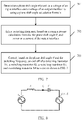
- fundamental wave analysis is performed on the circuit in FIG. 3 , to obtain a circuit equivalent model shown in FIG. 8 and a vector diagram shown in FIG. 9 .
- FIG. 8 is a diagram of a circuit equivalent model of fundamental wave analysis of the circuit corresponding to FIG. 3 according to an embodiment of this application.
- FIG. 9 is a vector diagram corresponding to FIG. 8 according to an embodiment of this application.
- Vp is an equivalent fundamental wave of an input voltage
- Vs' is an equivalent fundamental wave of an output voltage
- ix is an equivalent fundamental wave of a resonant cavity current.
- a minimum effective current value may be obtained by using a phase shift angle that meets the phase shift angle calculation formula, so that a phase of the resonant cavity current ix shown in FIG. 9 is between a voltage phase of Vp and a voltage phase of Vs'.
- the phase shift angle ⁇ may be adjusted, so that the phase of the resonant cavity current is between the voltage phase of Vp and the voltage phase of Vs'.
- ZVS zero voltage switching
- ZCS zero current switching
- Both the ZVS and the ZCS are soft switching, and mean that a semiconductor switch component implements zero voltage switching on or zero current switching off. In this case, a switching loss is low. Oscillation excited in a switching process can also be reduced, so that switching frequency can be greatly increased, facilitating miniaturization and modularization of a DCDC converter.
- a phase shift angle ⁇ that can implement full-range ZVS may be first selected based on the voltage of the input interface and the voltage of the output interface, to ensure that the switching transistor S1, the switching transistor S2, the switching transistor S3, and the switching transistor S4 can implement full-power-range ZVS.
- a frequency adjustment unit may be disposed to perform step 702.
- the frequency adjustment unit may be connected to a phase shift angle adjustment unit to obtain parameters such as the phase shift angle, the voltage of the input interface, and the voltage of the output interface. After calculating the switching frequency, the frequency adjustment unit may send the switching frequency and the phase shift angle to a control unit.
- the frequency adjustment unit may directly calculate the switching frequency based on required target power of the output interface and the output power calculation formula.
- the switching frequency may be a quantity of switching times of the switching transistor S1, the switching transistor S2, the switching transistor S3, or the switching transistor S4 in one period.
- the switching transistor S1, the switching transistor S2, the switching transistor S3, and the switching transistor S4 may have same switching frequency.
- the frequency adjustment unit may adjust the switching frequency, and calculate the power of the output interface in real time based on the output power calculation formula.
- a current value of the switching frequency is determined.
- the frequency adjustment unit may adjust the switching frequency, control, by using the control unit, on and off of the switching transistor S1, the switching transistor S2, the switching transistor S3, and the switching transistor S4 based on parameters such as the switching frequency and the phase shift angle that are obtained after adjustment, detect, in real time, the voltage and the current of the output interface by using a voltage detection module and a current detection module, and calculate the power of the output interface based on the detected voltage and the detected current.
- the power of the output interface may alternatively be directly detected by a power sensor. When the power of the output interface reaches a required target value (or within a threshold range close to the target value), a current value of the switching frequency is determined.
- the frequency adjustment unit may adjust the switching frequency again, so that the power of the output interface reaches the required output power again. For example, when the required output power changes to second target output power, the frequency adjustment unit may adjust the switching frequency based on the phase shift angle ⁇ and second target power of the output interface until the power of the output interface reaches the second target power.
- An adjustment method is similar to that in the foregoing embodiment, and details are not described herein again. Similarly, when a required output current changes, similar adjustment may also be performed, and details are not described herein again.
- the switching frequency may be determined by using the current of the output interface and the output power calculation formula. Specifically, in the control method, the power of the output interface is calculated based on the current of the output interface and the voltage of the output interface. After the power of the output interface is obtained, in the control method, switching frequency of the switching transistor S1, switching frequency of the switching transistor S2, switching frequency of the switching transistor S3, and switching frequency of the switching transistor S4 may be determined based on the power of the output interface and the output power calculation formula. This is similar to that in the foregoing embodiment, and details are not described herein again.
- step 701 and step 702 have no sequential relationship; in other words, the phase shift angle and the switching frequency may be adjusted simultaneously, so that both the voltage and the power of the output interface reach required values.
- a manner of determining the phase shift angle and the switching frequency may be: directly performing calculation by using a formula; may be: calculating the voltage and the power of the output interface in real time by adjusting the phase shift angle and the switching frequency, until both the voltage and the power of the output interface reach the required values; or may be: monitoring the voltage and the power of the output interface in real time by adjusting the phase shift angle and the switching frequency, until the voltage and the power of the output interface reach the required values. Details are not described in this embodiment of this application.
- step 701 and step 702 may be performed by a determining module to obtain the phase shift angle ⁇ and the switching frequency. Then, the determining module sends the phase shift angle ⁇ and the switching frequency to the control unit, so that the control unit controls, based on the phase shift angle ⁇ and the switching frequency, on and off of the switching transistor S1, the switching transistor S2, the switching transistor S3, and the switching transistor S4 in the circuit shown in FIG. 3 .
- a voltage detection unit, a current detection unit, and a power detection unit may be disposed for the determining module, to detect the voltage, the current, and the power of the output interface.
- control unit may directly perform step 701 and step 702 to obtain the phase shift angle ⁇ and the switching frequency, and then directly control, based on the phase shift angle ⁇ and the switching frequency, on and off of the switching transistor S 1, the switching transistor S2, the switching transistor S3, and the switching transistor S4 in the circuit shown in FIG. 3 .
- a voltage detection unit, a current detection unit, and a power detection unit may be disposed for the control unit, to detect the voltage, the current, and the power of the output interface.
- the control unit is a circuit component connecting the switching transistor S1, the switching transistor S2, the switching transistor S3, and the switching transistor S4, and may control on and off of the switching transistor S1, the switching transistor S2, the switching transistor S3, and the switching transistor S4 by using a drive signal.
- a drive signal For example, in the drive signal, a high level is used to turn on the switching transistor, and a low level is used to turn off the switching transistor.
- a voltage of a connection line connecting the control unit and the switching transistor S1 becomes a high level
- the switching transistor S1 is on.
- the control unit may alternatively control on and off of the switching transistor S1, the switching transistor S2, the switching transistor S3, and the switching transistor S4 in another manner. This is not limited in this embodiment of this application.
- the control unit controls, based on the phase shift angle ⁇ and the switching frequency, on and off of the switching transistor S1, the switching transistor S2, the switching transistor S3, and the switching transistor S4 in the circuit shown in FIG. 3 .
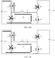
- a process is shown in FIG. 10a , FIG. 10b , FIG. 10c , FIG. 10d , FIG. 10e , and FIG. 10f .
- FIG. 10a is a schematic diagram 1 of a working principle of a non-isolated DCDC resonant conversion control circuit according to an embodiment of this application.
- An initial state of the non-isolated DCDC resonant conversion control circuit shown in FIG. 3 in embodiments of this application is shown in FIG. 10a .
- the switching transistor S2 and the switching transistor S4 are on, and a resonant cavity current flows in an anticlockwise direction.
- FIG. 10b is a schematic diagram 2 of a working principle of a non-isolated DCDC resonant conversion control circuit according to an embodiment of this application. Based on the circuit shown in FIG. 10a , if the control unit controls the switching transistor S2 to be off, a diode that is anti-parallel connected to the switching transistor S1 is on. In this case, the control unit controls the switching transistor S1 to be on, so that the switching transistor S1 can implement ZVS on, as shown in FIG. 10b .
- FIG. 10c is a schematic diagram 3 of a working principle of a non-isolated DCDC resonant conversion control circuit according to an embodiment of this application.
- the switching transistor S1 implements ZVS on
- the resonant cavity current flows in a clockwise direction, and a current of a positive electrode of the input interface sequentially flows to the switching transistor S1, the inductor L, the capacitor C, and the switching transistor S4, and then flows back to a negative electrode of the input interface, as shown in FIG. 10c .
- FIG. 10d is a schematic diagram 4 of a working principle of a non-isolated DCDC resonant conversion control circuit according to an embodiment of this application. Based on the circuit shown in FIG. 10c , if the control unit controls the switching transistor S4 to be off, a diode that is anti-parallel connected to the switching transistor S3 is on. In this case, the control unit controls the switching transistor S3 to be on, so that the switching transistor S3 can implement ZVS on, as shown in FIG. 10d .
- FIG. 10e is a schematic diagram 5 of a working principle of a non-isolated DCDC resonant conversion control circuit according to an embodiment of this application. Based on the circuit shown in FIG. 10d , if the control unit controls the switching transistor S1 to be off, a diode that is anti-parallel connected to the switching transistor S2 is on. In this case, the control unit controls the switching transistor S2 to be on, so that the switching transistor S2 can implement ZVS on, as shown in FIG. 10e .
- FIG. 10f is a schematic diagram 6 of a working principle of a non-isolated DCDC resonant conversion control circuit according to an embodiment of this application. Based on the circuit shown in FIG. 10e , after the switching transistor S2 implements ZVS on, the resonant cavity current flows in an anticlockwise direction, as shown in FIG. 10f .
- control unit controls the switching transistor S3 to be off, a diode that is anti-parallel connected to the switching transistor S4 is on. In this case, the control unit controls the switching transistor S4 to be on, so that the switching transistor S4 can implement ZVS on, as shown in FIG. 10a .
- the control unit when the control unit controls the switching transistor S1 to be on, the control unit controls the switching transistor S2 to be off; when the control unit controls the switching transistor S1 to be off, the control unit controls the switching transistor S2 to be on; when the control unit controls the switching transistor S3 to be on, the control unit controls the switching transistor S4 to be off; and when the control unit controls the switching transistor S3 to be off, the control unit controls the switching transistor S4 to be on.
- the control unit controls the switching transistor S1, the switching transistor S2, the switching transistor S3, and the switching transistor S4 to be continuously on and off.
- a quantity of turn-on times and a quantity of turn-off times of the switching transistor S1 are referred to as switching frequency of the switching transistor S1.
- the switching transistor S1, the switching transistor S2, the switching transistor S3, and the switching transistor S4 may have same switching frequency. For example, time used by the processes shown in FIG. 10a , FIG. 10b , FIG. 10c , FIG. 10d , FIG.
- the switching frequency of the switching transistor S1 is twice/millisecond, where one time is the quantity of turn-on times, and the other time is the quantity of turn-off times. If the switching frequency obtained by the control unit is once/millisecond, the control unit may reduce an on/off rate of the switching transistor, to prolong the time used by the processes shown in FIG. 10a , FIG. 10b , FIG. 10c , FIG. 10d , FIG. 10e , and FIG. 10f , so that the used time is prolonged to two milliseconds, and the switching frequency of the switching transistor S 1 changes to once/millisecond.
- FIG. 10a is a diagram of a working waveform of the circuit shown in FIG. 3 according to an embodiment of this application.
- VS1 is a voltage of a drive signal of the switch transistor S1
- VS3 is a voltage of a drive signal of the switching transistor S3
- VS1 and VS3 are complementary signals.
- VAO is a voltage from an end A to an end O
- VBO is a voltage from an end B to the end O.
- a current IL flowing through the inductor L is a sine waveform, and a waveform coefficient of a sine wave is small, and a conduction loss is low. Therefore, the circuit provided in this embodiment of this application can significantly reduce a circuit loss.
- FIG. 12 is a schematic diagram of a control policy for the circuit in FIG. 3 according to an embodiment of this application. It can be learned that, in this embodiment of this application, after the voltage of the input interface and the voltage of the output interface are obtained, a proper phase shift angle may be determined. Then, the switching frequency of the switching transistor S1, the switching frequency of the switching transistor S2, the switching frequency of the switching transistor S3, and the switching frequency of the switching transistor S4 are determined based on the phase shift angle and the power or the current of the output interface. Finally, on and off of the switching transistor S1, the switching transistor S2, the switching transistor S3, and the switching transistor S4 are controlled based on the determined phase shift angle and the determined switching frequency.
- the phase shift angle adjustment unit, the frequency adjustment unit, and the control unit may be used for implementation.
- the control unit is connected to the switching transistor S 1, the switching transistor S2, the switching transistor S3, and the switching transistor S4, and may control on and off of the switching transistor S1, the switching transistor S2, the switching transistor S3, and the switching transistor S4 by using a drive signal.
- the phase shift angle adjustment unit is connected to the input interface and the output interface, and is configured to: determine the phase shift angle ⁇ based on the voltage of the input interface and the voltage of the output interface by using the phase shift angle calculation formula, and then send parameters such as an input voltage, an output voltage, and the phase shift angle ⁇ to the frequency adjustment unit.
- the frequency adjustment unit is connected to the output interface and the phase shift angle adjustment unit, and is configured to: adjust the switching frequency based on the output power calculation formula, the phase shift angle ⁇ , and the power or the current of the output interface, and then send the phase shift angle ⁇ and the switching frequency to the control unit.
- a reference current is coupled and input between the frequency adjustment unit and the output interface, and is used as a current inner loop to perform loop control, to ensure system stability.
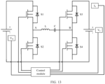
- FIG. 13 is a schematic diagram of a circuit including a control module according to an embodiment of this application.
- FIG. 14 is a schematic diagram of a power supply system according to an embodiment of this application.
- the power supply system specifically includes a power supply module and the non-isolated DCDC resonant conversion control circuit in any one of the foregoing embodiments.
- An output end of the power module is connected to an input interface in the non-isolated DCDC resonant conversion control circuit.
- An output interface in the non-isolated DCDC resonant conversion control circuit is connected to a load.
- the non-isolated DCDC resonant conversion control circuit may be adjusted, so that an output voltage of the output interface in the non-isolated DCDC resonant conversion control circuit is 12 V, to meet a requirement of the load.
- the power supply module is specifically a lithium battery, and has advantages of relatively high energy, a long service life, and being environmental friendly.
- the power supply module is specifically a photovoltaic power supply.
- This embodiment of this application is mainly applied to an application scenario in which there is a non-isolated DCDC conversion requirement, such as lithium battery DCDC conversion, battery DCDC conversion, or photovoltaic front-stage DCDC conversion, and may be used as a DCDC conversion power supply.
- An application scenario is not limited in this embodiment of this application.
- the disclosed system, apparatus, and method may be implemented in other manners.
- the described apparatus embodiment is merely an example.
- the unit division is merely logical function division and may be other division in actual implementation.
- a plurality of units or components may be combined or integrated into another system, or some features may be ignored or not performed.
- the displayed or discussed mutual couplings or direct couplings or communication connections may be implemented by using some interfaces.
- the indirect couplings or communication connections between the apparatuses or units may be implemented in electronic, mechanical, or other forms.
- the units described as separate parts may or may not be physically separate, and parts displayed as units may or may not be physical units, may be located in one position, or may be distributed on a plurality of network units. Some or all of the units may be selected based on actual requirements to achieve the objectives of the solutions of the embodiments.
- functional units in embodiments of this application may be integrated into one processing unit, or each of the units may exist alone physically, or two or more units may be integrated into one unit.
- the integrated unit may be implemented in a form of hardware, or may be implemented in a form of a software functional unit.
- the integrated unit When the integrated unit is implemented in the form of the software functional unit and sold or used as an independent product, the integrated unit may be stored in a computer-readable storage medium.
- the computer software product is stored in a storage medium and includes several instructions for instructing a computer device (which may be a personal computer, a server, or a network device) to perform all or some of the steps of the methods described in embodiments of this application.
- the foregoing storage medium includes any medium that can store program code, such as a USB flash drive, a removable hard disk, a read-only memory (ROM), a random access memory (RAM), a magnetic disk, or an optical disc.
Landscapes
- Engineering & Computer Science (AREA)
- Power Engineering (AREA)
- Dc-Dc Converters (AREA)
- Inverter Devices (AREA)
Applications Claiming Priority (2)
| Application Number | Priority Date | Filing Date | Title |
|---|---|---|---|
| CN202010360907.4A CN111614256B (zh) | 2020-04-29 | 2020-04-29 | 一种非隔离dcdc谐振变换控制电路及控制方法 |
| PCT/CN2021/087996 WO2021218678A1 (fr) | 2020-04-29 | 2021-04-19 | Circuit de commande de conversion résonnante cc-cc non isolée, et procédé de commande |
Publications (3)
| Publication Number | Publication Date |
|---|---|
| EP4131761A1 true EP4131761A1 (fr) | 2023-02-08 |
| EP4131761A4 EP4131761A4 (fr) | 2023-08-23 |
| EP4131761B1 EP4131761B1 (fr) | 2025-11-12 |
Family
ID=72202944
Family Applications (1)
| Application Number | Title | Priority Date | Filing Date |
|---|---|---|---|
| EP21797135.7A Active EP4131761B1 (fr) | 2020-04-29 | 2021-04-19 | Circuit de commande de conversion résonnante cc-cc non isolée, et procédé de commande |
Country Status (4)
| Country | Link |
|---|---|
| US (1) | US12267014B2 (fr) |
| EP (1) | EP4131761B1 (fr) |
| CN (1) | CN111614256B (fr) |
| WO (1) | WO2021218678A1 (fr) |
Families Citing this family (3)
| Publication number | Priority date | Publication date | Assignee | Title |
|---|---|---|---|---|
| CN111614256B (zh) | 2020-04-29 | 2022-04-05 | 华为技术有限公司 | 一种非隔离dcdc谐振变换控制电路及控制方法 |
| CN113904551B (zh) * | 2021-11-10 | 2025-09-16 | 浙江大学杭州国际科创中心 | 一种极性变换器的控制方法、装置、设备及可读存储介质 |
| CN114552715A (zh) * | 2022-03-01 | 2022-05-27 | 英华达(上海)科技有限公司 | 供电系统 |
Family Cites Families (33)
| Publication number | Priority date | Publication date | Assignee | Title |
|---|---|---|---|---|
| US6337801B2 (en) * | 1999-12-16 | 2002-01-08 | Virginia Tech Intellectual Properties, Inc. | Three-phase zero-current-transition (ZCT) inverters and rectifiers with three auxiliary switches |
| US6246599B1 (en) * | 2000-08-25 | 2001-06-12 | Delta Electronics, Inc. | Constant frequency resonant inverters with a pair of resonant inductors |
| CN2691158Y (zh) * | 2003-10-27 | 2005-04-06 | 杭州中恒电气股份有限公司 | Dc/dc全桥移相电力调压模块 |
| US7212419B2 (en) * | 2004-02-24 | 2007-05-01 | Vlt, Inc. | Adaptively configured and autoranging voltage transformation module arrays |
| US7796406B2 (en) * | 2007-07-31 | 2010-09-14 | Lumenis Ltd. | Apparatus and method for high efficiency isolated power converter |
| JP5424307B2 (ja) * | 2009-05-07 | 2014-02-26 | 田淵電機株式会社 | 絶縁型dc−dcコンバータ |
| CN102651563B (zh) * | 2011-02-25 | 2014-06-18 | 香港理工大学 | 电池能量平衡电路 |
| CN102158096B (zh) * | 2011-05-11 | 2013-11-20 | 南京博兰得电子科技有限公司 | 一种非隔离式谐振变换器 |
| CN103078492A (zh) * | 2011-10-26 | 2013-05-01 | 中兴通讯股份有限公司 | 谐振变换器的控制方法和装置 |
| CN102647030B (zh) * | 2012-03-31 | 2014-11-05 | 海尔集团公司 | 无线电能发射装置及无线电能供电系统 |
| JP5939903B2 (ja) * | 2012-06-22 | 2016-06-22 | 日立アプライアンス株式会社 | 電磁誘導加熱装置 |
| KR20150048875A (ko) * | 2012-09-03 | 2015-05-07 | 로베르트 보쉬 (에스이에이) 프라이빗 리미티드 | 하이브리드 저장 시스템들을 위한 토폴로지 및 제어 계획 |
| US9490719B2 (en) * | 2013-12-18 | 2016-11-08 | Infineon Technologies Ag | System and method for a power converter |
| US9748843B2 (en) * | 2014-09-24 | 2017-08-29 | Linear Technology Corporation | DCR inductor current-sensing in four-switch buck-boost converters |
| CN204304528U (zh) * | 2014-12-19 | 2015-04-29 | 山东大学 | 基于Buck-Boost变换和双向LC谐振变换的均衡电路 |
| CN105048602B (zh) * | 2015-08-31 | 2017-12-05 | 矽力杰半导体技术(杭州)有限公司 | 电池平衡电路及电池装置 |
| US9793810B2 (en) * | 2015-09-10 | 2017-10-17 | Futurewei Technologies, Inc. | Control method for zero voltage switching buck-boost power converters |
| US10137788B2 (en) * | 2015-09-16 | 2018-11-27 | General Electric Company | Power electronic device and method |
| CN106026645B (zh) * | 2016-07-20 | 2018-08-14 | 南京航空航天大学 | 一种双向谐振变换器及其控制方法 |
| CN108347167B (zh) * | 2017-01-25 | 2021-07-13 | 通用电气公司 | 用于软切换dc—dc转换器的系统和方法 |
| US10965206B2 (en) * | 2017-03-13 | 2021-03-30 | Rohm Co., Ltd. | Step-up/down DC-DC converter |
| CN108054918B (zh) * | 2017-11-20 | 2020-04-03 | 华为数字技术(苏州)有限公司 | 一种四管buck-boost电路的控制方法、控制电路及系统 |
| CN108075668B (zh) * | 2017-12-14 | 2020-02-07 | 东南大学 | 串联谐振全桥变换器的变频移相非对称占空比调制方法 |
| CN109980929A (zh) * | 2017-12-27 | 2019-07-05 | 弗莱克斯有限公司 | 具有电压变换器控制的准谐振降压-升压转换器 |
| CN107959421B (zh) * | 2017-12-28 | 2020-03-17 | 北京松果电子有限公司 | Buck-boost型直流转换器及其控制方法 |
| CN108539980B (zh) * | 2018-05-18 | 2020-03-20 | 湖北工程学院 | 一种双向dc/dc变换器 |
| WO2019224431A1 (fr) * | 2018-05-24 | 2019-11-28 | Vensum Power Oy | Convertisseurs de puissance à commutation au zéro de la tension |
| EP3595155A1 (fr) * | 2018-07-10 | 2020-01-15 | Siemens Aktiengesellschaft | Unité de commande pour produire une puissance variable de sortie d'un circuit en pont commutant résonant |
| CN109698626A (zh) * | 2018-12-18 | 2019-04-30 | 东南大学 | 一种适用于中压直流配电网的组合式输入串联输出并联直流变压器及其控制方法 |
| CN109802568A (zh) * | 2019-03-19 | 2019-05-24 | 深圳市凌康技术有限公司 | 一种可变结构与参数自整定的宽范围输出功率变换器 |
| CN110601543B (zh) * | 2019-09-11 | 2020-08-18 | 广州金升阳科技有限公司 | 一种llc谐振变换器的宽增益控制方法及其谐振变换器 |
| CN110729906A (zh) * | 2019-11-18 | 2020-01-24 | 陕西科技大学 | 一种零电压转换cll谐振dc-dc变换器及其控制方法 |
| CN111614256B (zh) * | 2020-04-29 | 2022-04-05 | 华为技术有限公司 | 一种非隔离dcdc谐振变换控制电路及控制方法 |
-
2020
- 2020-04-29 CN CN202010360907.4A patent/CN111614256B/zh active Active
-
2021
- 2021-04-19 EP EP21797135.7A patent/EP4131761B1/fr active Active
- 2021-04-19 WO PCT/CN2021/087996 patent/WO2021218678A1/fr not_active Ceased
-
2022
- 2022-10-28 US US17/976,010 patent/US12267014B2/en active Active
Also Published As
| Publication number | Publication date |
|---|---|
| US12267014B2 (en) | 2025-04-01 |
| EP4131761B1 (fr) | 2025-11-12 |
| CN111614256A (zh) | 2020-09-01 |
| CN111614256B (zh) | 2022-04-05 |
| WO2021218678A1 (fr) | 2021-11-04 |
| US20230053061A1 (en) | 2023-02-16 |
| EP4131761A4 (fr) | 2023-08-23 |
Similar Documents
| Publication | Publication Date | Title |
|---|---|---|
| US12267014B2 (en) | Non-isolated DCDC resonant conversion control circuit and control method | |
| Rodriguez et al. | Different purpose design strategies and techniques to improve the performance of a dual active bridge with phase-shift control | |
| CN202997663U (zh) | 稳压恒流充电控制电路 | |
| CN112600432B (zh) | 一种llc谐振变换器预测电荷控制方法 | |
| CN114448248B (zh) | 耦合电感交错并联四开关升降压双向变换器的控制电路 | |
| CN119315803B (zh) | 一种级联系统的同步零电压调制系统方法、介质及设备 | |
| WO2023087826A1 (fr) | Circuit de charge sans fil, circuit de commutation, procédé de commande et support de stockage | |
| CN116647134A (zh) | V2g直流充放电器及控制方法 | |
| CN113765408B (zh) | 基于预测控制的dab变换器关断损耗优化控制方法及系统 | |
| Mohajery et al. | A modified configuration of high step‐up non‐isolated DC‐DC converter with low voltage stress: Analysis, design, and implementation | |
| EP4622082A1 (fr) | Circuit d'alimentation électrique et appareil approprié pour une sortie à large plage, système et procédé de commande | |
| CN118826499B (zh) | 一种用于弱励磁条件下dcdc全桥变换器的控制系统及方法 | |
| CN120090465A (zh) | 一种四开关升降压变换器效率优化的控制器及控制方法 | |
| Chen et al. | Predictive charge control for LLC resonant converters | |
| CN118074492A (zh) | 双向dc-dc电源可变频率的软开关控制方法 | |
| Wang et al. | A new modeling method for burst mode with three-pulse trajectory control of CLLC resonant converter | |
| CN117439372A (zh) | 一种dab变换器多目标优化调制方法 | |
| Li et al. | Burst FM control of LLC resonant converter with multiplier for high efficiency and low ripple in TWT power supply | |
| CN103546019B (zh) | 电力电子变换器的能量平衡控制器及方法 | |
| Xu et al. | An Improved Model Predictive Control Approach for Wireless Power Transfer System of Electric Vehicles | |
| WO2023024998A1 (fr) | Circuit de réglage de puissance, procédé et appareil, et produit associé | |
| CN102005927B (zh) | 用查表法修正串联谐振开关变换器谐振漂移的装置及方法 | |
| CN114696616A (zh) | 基于差分连接的三端口高增益升压dc/dc变换器及其控制方法 | |
| CN201893704U (zh) | 用查表法修正串联谐振开关变换器谐振漂移的装置 | |
| Subramanian et al. | Analysis of dual-input three-port isolated DC–DC converter with bidirectional capability |
Legal Events
| Date | Code | Title | Description |
|---|---|---|---|
| STAA | Information on the status of an ep patent application or granted ep patent |
Free format text: STATUS: THE INTERNATIONAL PUBLICATION HAS BEEN MADE |
|
| PUAI | Public reference made under article 153(3) epc to a published international application that has entered the european phase |
Free format text: ORIGINAL CODE: 0009012 |
|
| STAA | Information on the status of an ep patent application or granted ep patent |
Free format text: STATUS: REQUEST FOR EXAMINATION WAS MADE |
|
| 17P | Request for examination filed |
Effective date: 20221028 |
|
| AK | Designated contracting states |
Kind code of ref document: A1 Designated state(s): AL AT BE BG CH CY CZ DE DK EE ES FI FR GB GR HR HU IE IS IT LI LT LU LV MC MK MT NL NO PL PT RO RS SE SI SK SM TR |
|
| DAV | Request for validation of the european patent (deleted) | ||
| DAX | Request for extension of the european patent (deleted) | ||
| A4 | Supplementary search report drawn up and despatched |
Effective date: 20230724 |
|
| RIC1 | Information provided on ipc code assigned before grant |
Ipc: H02M 3/158 20060101ALI20230718BHEP Ipc: H02M 3/00 20060101ALI20230718BHEP Ipc: H02M 1/00 20060101ALI20230718BHEP Ipc: H02M 3/07 20060101AFI20230718BHEP |
|
| STAA | Information on the status of an ep patent application or granted ep patent |
Free format text: STATUS: EXAMINATION IS IN PROGRESS |
|
| 17Q | First examination report despatched |
Effective date: 20250211 |
|
| GRAP | Despatch of communication of intention to grant a patent |
Free format text: ORIGINAL CODE: EPIDOSNIGR1 |
|
| STAA | Information on the status of an ep patent application or granted ep patent |
Free format text: STATUS: GRANT OF PATENT IS INTENDED |
|
| INTG | Intention to grant announced |
Effective date: 20250610 |
|
| GRAS | Grant fee paid |
Free format text: ORIGINAL CODE: EPIDOSNIGR3 |
|
| P01 | Opt-out of the competence of the unified patent court (upc) registered |
Free format text: CASE NUMBER: UPC_APP_5360_4131761/2025 Effective date: 20250829 |
|
| GRAA | (expected) grant |
Free format text: ORIGINAL CODE: 0009210 |
|
| STAA | Information on the status of an ep patent application or granted ep patent |
Free format text: STATUS: THE PATENT HAS BEEN GRANTED |
|
| AK | Designated contracting states |
Kind code of ref document: B1 Designated state(s): AL AT BE BG CH CY CZ DE DK EE ES FI FR GB GR HR HU IE IS IT LI LT LU LV MC MK MT NL NO PL PT RO RS SE SI SK SM TR |
|
| REG | Reference to a national code |
Ref country code: CH Ref legal event code: F10 Free format text: ST27 STATUS EVENT CODE: U-0-0-F10-F00 (AS PROVIDED BY THE NATIONAL OFFICE) Effective date: 20251112 Ref country code: GB Ref legal event code: FG4D |
|
| REG | Reference to a national code |
Ref country code: IE Ref legal event code: FG4D |
|
| REG | Reference to a national code |
Ref country code: DE Ref legal event code: R096 Ref document number: 602021042317 Country of ref document: DE |
|
| REG | Reference to a national code |
Ref country code: NL Ref legal event code: MP Effective date: 20251112 |
|
| PG25 | Lapsed in a contracting state [announced via postgrant information from national office to epo] |
Ref country code: ES Free format text: LAPSE BECAUSE OF FAILURE TO SUBMIT A TRANSLATION OF THE DESCRIPTION OR TO PAY THE FEE WITHIN THE PRESCRIBED TIME-LIMIT Effective date: 20251112 |
|
| REG | Reference to a national code |
Ref country code: LT Ref legal event code: MG9D |
|
| PG25 | Lapsed in a contracting state [announced via postgrant information from national office to epo] |
Ref country code: NO Free format text: LAPSE BECAUSE OF FAILURE TO SUBMIT A TRANSLATION OF THE DESCRIPTION OR TO PAY THE FEE WITHIN THE PRESCRIBED TIME-LIMIT Effective date: 20260212 |
|
| PG25 | Lapsed in a contracting state [announced via postgrant information from national office to epo] |
Ref country code: FI Free format text: LAPSE BECAUSE OF FAILURE TO SUBMIT A TRANSLATION OF THE DESCRIPTION OR TO PAY THE FEE WITHIN THE PRESCRIBED TIME-LIMIT Effective date: 20251112 Ref country code: AT Free format text: LAPSE BECAUSE OF FAILURE TO SUBMIT A TRANSLATION OF THE DESCRIPTION OR TO PAY THE FEE WITHIN THE PRESCRIBED TIME-LIMIT Effective date: 20251112 Ref country code: HR Free format text: LAPSE BECAUSE OF FAILURE TO SUBMIT A TRANSLATION OF THE DESCRIPTION OR TO PAY THE FEE WITHIN THE PRESCRIBED TIME-LIMIT Effective date: 20251112 |
|
| REG | Reference to a national code |
Ref country code: AT Ref legal event code: MK05 Ref document number: 1857649 Country of ref document: AT Kind code of ref document: T Effective date: 20251112 |
|
| PG25 | Lapsed in a contracting state [announced via postgrant information from national office to epo] |
Ref country code: NL Free format text: LAPSE BECAUSE OF FAILURE TO SUBMIT A TRANSLATION OF THE DESCRIPTION OR TO PAY THE FEE WITHIN THE PRESCRIBED TIME-LIMIT Effective date: 20251112 |
|
| PG25 | Lapsed in a contracting state [announced via postgrant information from national office to epo] |
Ref country code: RS Free format text: LAPSE BECAUSE OF FAILURE TO SUBMIT A TRANSLATION OF THE DESCRIPTION OR TO PAY THE FEE WITHIN THE PRESCRIBED TIME-LIMIT Effective date: 20260212 |
|
| PG25 | Lapsed in a contracting state [announced via postgrant information from national office to epo] |
Ref country code: IS Free format text: LAPSE BECAUSE OF FAILURE TO SUBMIT A TRANSLATION OF THE DESCRIPTION OR TO PAY THE FEE WITHIN THE PRESCRIBED TIME-LIMIT Effective date: 20260312 |
|
| PG25 | Lapsed in a contracting state [announced via postgrant information from national office to epo] |
Ref country code: PT Free format text: LAPSE BECAUSE OF FAILURE TO SUBMIT A TRANSLATION OF THE DESCRIPTION OR TO PAY THE FEE WITHIN THE PRESCRIBED TIME-LIMIT Effective date: 20260312 |
|
| PG25 | Lapsed in a contracting state [announced via postgrant information from national office to epo] |
Ref country code: PL Free format text: LAPSE BECAUSE OF FAILURE TO SUBMIT A TRANSLATION OF THE DESCRIPTION OR TO PAY THE FEE WITHIN THE PRESCRIBED TIME-LIMIT Effective date: 20251112 |
|
| PG25 | Lapsed in a contracting state [announced via postgrant information from national office to epo] |
Ref country code: LV Free format text: LAPSE BECAUSE OF FAILURE TO SUBMIT A TRANSLATION OF THE DESCRIPTION OR TO PAY THE FEE WITHIN THE PRESCRIBED TIME-LIMIT Effective date: 20251112 |