EP4131783A1 - Ausgangstreiberschaltung und speicher - Google Patents
Ausgangstreiberschaltung und speicher Download PDFInfo
- Publication number
- EP4131783A1 EP4131783A1 EP21773281.7A EP21773281A EP4131783A1 EP 4131783 A1 EP4131783 A1 EP 4131783A1 EP 21773281 A EP21773281 A EP 21773281A EP 4131783 A1 EP4131783 A1 EP 4131783A1
- Authority
- EP
- European Patent Office
- Prior art keywords
- pull
- terminal
- output
- signal
- unit
- Prior art date
- Legal status (The legal status is an assumption and is not a legal conclusion. Google has not performed a legal analysis and makes no representation as to the accuracy of the status listed.)
- Withdrawn
Links
Images

Classifications
-
- H—ELECTRICITY
- H03—ELECTRONIC CIRCUITRY
- H03K—PULSE TECHNIQUE
- H03K19/00—Logic circuits, i.e. having at least two inputs acting on one output; Inverting circuits
- H03K19/0175—Coupling arrangements; Interface arrangements
- H03K19/017509—Interface arrangements
-
- H—ELECTRICITY
- H03—ELECTRONIC CIRCUITRY
- H03K—PULSE TECHNIQUE
- H03K19/00—Logic circuits, i.e. having at least two inputs acting on one output; Inverting circuits
- H03K19/20—Logic circuits, i.e. having at least two inputs acting on one output; Inverting circuits characterised by logic function, e.g. AND, OR, NOR, NOT circuits
-
- G—PHYSICS
- G11—INFORMATION STORAGE
- G11C—STATIC STORES
- G11C11/00—Digital stores characterised by the use of particular electric or magnetic storage elements; Storage elements therefor
- G11C11/21—Digital stores characterised by the use of particular electric or magnetic storage elements; Storage elements therefor using electric elements
- G11C11/34—Digital stores characterised by the use of particular electric or magnetic storage elements; Storage elements therefor using electric elements using semiconductor devices
- G11C11/40—Digital stores characterised by the use of particular electric or magnetic storage elements; Storage elements therefor using electric elements using semiconductor devices using transistors
- G11C11/401—Digital stores characterised by the use of particular electric or magnetic storage elements; Storage elements therefor using electric elements using semiconductor devices using transistors forming cells needing refreshing or charge regeneration, i.e. dynamic cells
- G11C11/4063—Auxiliary circuits, e.g. for addressing, decoding, driving, writing, sensing or timing
- G11C11/407—Auxiliary circuits, e.g. for addressing, decoding, driving, writing, sensing or timing for memory cells of the field-effect type
- G11C11/409—Read-write [R-W] circuits
- G11C11/4096—Input/output [I/O] data management or control circuits, e.g. reading or writing circuits, I/O drivers or bit-line switches
-
- G—PHYSICS
- G11—INFORMATION STORAGE
- G11C—STATIC STORES
- G11C29/00—Checking stores for correct operation ; Subsequent repair; Testing stores during standby or offline operation
- G11C29/02—Detection or location of defective auxiliary circuits, e.g. defective refresh counters
- G11C29/022—Detection or location of defective auxiliary circuits, e.g. defective refresh counters in I/O circuitry
-
- G—PHYSICS
- G11—INFORMATION STORAGE
- G11C—STATIC STORES
- G11C29/00—Checking stores for correct operation ; Subsequent repair; Testing stores during standby or offline operation
- G11C29/02—Detection or location of defective auxiliary circuits, e.g. defective refresh counters
- G11C29/028—Detection or location of defective auxiliary circuits, e.g. defective refresh counters with adaption or trimming of parameters
-
- G—PHYSICS
- G11—INFORMATION STORAGE
- G11C—STATIC STORES
- G11C29/00—Checking stores for correct operation ; Subsequent repair; Testing stores during standby or offline operation
- G11C29/04—Detection or location of defective memory elements, e.g. cell constructio details, timing of test signals
- G11C29/50—Marginal testing, e.g. race, voltage or current testing
- G11C29/50012—Marginal testing, e.g. race, voltage or current testing of timing
-
- G—PHYSICS
- G11—INFORMATION STORAGE
- G11C—STATIC STORES
- G11C7/00—Arrangements for writing information into, or reading information out from, a digital store
- G11C7/10—Input/output [I/O] data interface arrangements, e.g. I/O data control circuits, I/O data buffers
- G11C7/1051—Data output circuits, e.g. read-out amplifiers, data output buffers, data output registers, data output level conversion circuits
- G11C7/1057—Data output buffers, e.g. comprising level conversion circuits, circuits for adapting load
-
- H—ELECTRICITY
- H03—ELECTRONIC CIRCUITRY
- H03K—PULSE TECHNIQUE
- H03K19/00—Logic circuits, i.e. having at least two inputs acting on one output; Inverting circuits
- H03K19/01—Modifications for accelerating switching
- H03K19/017—Modifications for accelerating switching in field-effect transistor circuits
- H03K19/01707—Modifications for accelerating switching in field-effect transistor circuits in asynchronous circuits
- H03K19/01721—Modifications for accelerating switching in field-effect transistor circuits in asynchronous circuits by means of a pull-up or down element
-
- H—ELECTRICITY
- H03—ELECTRONIC CIRCUITRY
- H03K—PULSE TECHNIQUE
- H03K19/00—Logic circuits, i.e. having at least two inputs acting on one output; Inverting circuits
- H03K19/0175—Coupling arrangements; Interface arrangements
-
- H—ELECTRICITY
- H03—ELECTRONIC CIRCUITRY
- H03K—PULSE TECHNIQUE
- H03K19/00—Logic circuits, i.e. having at least two inputs acting on one output; Inverting circuits
- H03K19/0175—Coupling arrangements; Interface arrangements
- H03K19/0185—Coupling arrangements; Interface arrangements using field effect transistors only
- H03K19/018507—Interface arrangements
-
- G—PHYSICS
- G11—INFORMATION STORAGE
- G11C—STATIC STORES
- G11C2207/00—Indexing scheme relating to arrangements for writing information into, or reading information out from, a digital store
- G11C2207/22—Control and timing of internal memory operations
- G11C2207/2254—Calibration
Definitions
- the present application relates to the field of integrated circuits, in particular to an output driving circuit and a memory.
- the technical problem to be solved by the present application is to provide an output driving circuit and a memory that can increase a slew rate of an output signal of the memory and then greatly increase a transmission rate of the memory.
- an output driving circuit including: a signal input terminal inputting a positive input signal and a negative input signal complementary to each other; a pull-up output unit connected to the signal input terminal, the positive input signal acting as an input signal of the pull-up output unit; a pull-down output unit connected to the signal input terminal, the negative input signal acting as an input signal of the pull-down output unit; at least one compensation unit connected in parallel with the pull-up output unit or the pull-down output unit; at least one pulse signal generation circuit having an input terminal connected to the signal input terminal, and generating a pulse signal based on the positive input signal or the negative input signal, the pulse signal acting as a control signal of the compensation unit; and a signal output terminal connected to an output terminal of the pull-up output unit, an output terminal of the pull-down output unit and an output terminal of the compensation unit, and outputting an output signal.
- a pulse width of the pulse signal is less than that of the positive input signal or the negative input signal.
- the pulse signal generation circuit generates the pulse signal through a rising edge or a falling edge of the positive input signal or the negative input signal.
- a pulse width of the pulse signal is less than or equal to a rising edge time or a falling edge time of the output signal.
- the pulse signal generation circuit includes a first delay branch, a second delay circuit and an AND circuit
- the first delay branch is connected in parallel with the second delay branch and then connected in series with the AND circuit
- the positive input signal or the negative input signal acts as input signals of the first delay branch and the second delay circuit
- output signals of the first delay branch and the second delay circuit acts as an input signal of the AND circuit together
- the AND circuit outputs the pulse signal
- the first delay branch and the second delay circuit have different delay times.
- the first delay branch includes at least a NOT gate and a first delay unit connected in series
- the second delay unit includes at least a second delay unit, and the delay times of the first delay branch and the second delay circuit are adjusted to change a pulse width of the pulse signal.
- the output driving circuit further includes at least one delay unit, the delay unit is arranged at the input terminal of the pulse signal generation circuit, and the positive input signal or the negative input signal is inputted to the pulse signal generation circuit through the delay unit.
- the output driving circuit includes two compensation units that are a pull-up compensation unit and a pull-down compensation unit respectively, the pull-up compensation unit is connected in parallel with the pull-up output unit, and the pull-down compensation unit is connected in parallel with the pull-down output unit.
- the output driving circuit includes two pulse signal generation circuits that are a pull-up pulse signal generation circuit and a pull-down pulse signal generation circuit respectively, the pull-up pulse signal generation circuit generates a first pulse signal based on the positive input signal, the first pulse signal acts as a control signal of the pull-up compensation unit, the pull-down pulse signal generation circuit generates a second pulse signal based on the negative input signal, and the second pulse signal acts as a control signal of the pull-down compensation unit.
- the pull-up output unit includes one first transistor or a plurality of first transistors arranged in parallel, the first transistor including a first terminal, a second terminal and a control terminal;
- the pull-up compensation unit includes one second transistor or a plurality of second transistors arranged in parallel, the second transistor including a first terminal, a second terminal and a control terminal; the first terminals of the first transistor and the second transistor are connected to a power supply voltage, the second terminals of the first transistor and the second transistor are connected to the signal output terminal, the control terminal of the first transistor is connected to the signal input terminal, and the control terminal of the second transistor is connected to the pull-up pulse signal generation circuit.
- the pull-down output unit includes one third transistor or a plurality of third transistors arranged in parallel, the third transistor including a first terminal, a second terminal and a control terminal;
- the pull-down compensation unit includes one fourth transistor or a plurality of fourth transistors arranged in parallel, the fourth transistor including a first terminal, a second terminal and a control terminal; the first terminals of the third transistor and the fourth transistor are grounded, the second terminals of the third transistor and the fourth transistor are connected to the signal output terminal, the control terminal of the third transistor is connected to the signal input terminal, and the control terminal of the fourth transistor is connected to the pull-down pulse signal generation circuit.
- the output driving circuit further includes a pull-up pre-amplification unit and a pull-down pre-amplification unit;
- the pull-up pre-amplification unit includes a first terminal and a second terminal, the first terminal is connected to the positive input signal, and the second terminal is connected to the control terminal of the pull-up output unit;
- the pull-down pre-amplification unit includes a first terminal and a second terminal, the first terminal is connected to the negative input signal, the second terminal is connected to the control terminal of the pull-down output unit, and the input terminal of the pulse signal generation circuit is connected to the second terminal of the pull-up pre-amplification unit or the second terminal of the pull-down pre-amplification unit.
- the output driving circuit further includes a pull-up impedance calibration unit and a pull-down impedance calibration unit, the pull-up impedance calibration unit is connected in parallel with the pull-up output unit, and the pull-down impedance calibration unit is connected in parallel with the pull-down output unit.
- the output driving circuit includes a plurality of parallel driving modules, the driving module including at least the signal input terminal, the pull-up output unit, the pull-down output unit, the compensation unit and the signal input terminal.
- the plurality of driving modules share the same pulse signal generation circuit.
- the present application further provides a memory including the output driving circuit as described above.
- the compensation unit is controlled to be turned on by using the pulse signal generated by the pulse signal generation circuit to add an additional current to the pull-up output unit or the pull-down output unit, so as to increase the slew rate of the output signal of the output driving circuit.
- An output signal of the pull-up compensation unit and an output signal of the pull-up output unit act as a positive output signal of the signal output terminal together, and an output signal of the pull-down compensation unit and an output signal of the pull-down output unit act as a negative output signal of the signal output terminal together.
- the compensation unit is controlled to be turned on through the pulse signal generation circuit, and then the pull-up output unit and the pull-down output unit are compensated, which increases a slew rate of an output signal finally outputted by additionally adding a current generated by the compensation unit while signal conversion is performed.
- Figure 1 is a schematic diagram of a first embodiment of an output driving circuit according to the present application.
- the output driving circuit according to the present application includes a signal input terminal 10, a pull-up output unit 20, a pull-down output unit 30, at least one pulse signal generation circuit, at least one compensation unit and a signal output terminal 60.
- the signal input terminal 10 can provide an input signal.
- the input signal includes a positive input signal Data_In_Pos and a negative input signal Data_In_Neg complementary to each other.
- the input signal is a signal after parallel-serial conversion by a pre-amplifier.
- the positive input signal Data_In_Pos and the negative input signal Data_In_Neg are set as complementary signals so that the pull-up output unit 20 and the pull-down output unit 30 are not turned on at the same time, so as to form an output signal DQ.
- One method for setting the positive input signal Data_In_Pos and the negative input signal Data_In_Neg to be complementary is to enable a control signal input terminal to directly output the positive input signal Data_In_Pos and the negative input signal Data_In_Neg complementary to each other.
- Another method is to set the pull-up output unit 20 and the pull-down output unit 30 to be of different transistor types so that an input signal of the pull-up output unit 20 and an input signal of the pull-down output unit 30 are complementary input signals.
- the pull-up output unit 20 is connected to the signal input terminal 10.
- the positive input signal Data_In_Pos acts as the input signal of the pull-up output unit 20.
- An output terminal of the pull-up output unit 20 is connected to the signal output terminal 60.
- the pull-up output unit 20 may consist of one first transistor or a plurality of parallel first transistors. Specifically, in this embodiment, the pull-up output unit 20 consists of one first transistor N1, and the first transistor N1 is an NMOS transistor.
- the first transistor N1 includes a first terminal, a second terminal and a control terminal.
- the first terminal of the first transistor N1 is a drain and connected to a power supply voltage
- the second terminal of the first transistor N1 is a source and connected to the signal output terminal 60
- the control terminal of the first transistor N1 is a gate and connected to the signal input terminal 10.
- the positive input signal Data_In_Pos acts as an input signal of the gate.
- the first transistor N1 may also be a PMOS transistor.
- the pull-down output unit 30 is connected to the signal input terminal 10.
- the negative input signal Data_In_Neg acts as the input signal of the pull-down output unit 30.
- An output terminal of the pull-down output unit 30 is connected to the signal output terminal 60.
- the pull-down output unit 30 may consist of one third transistor N3 or a plurality of parallel third transistors N3. Specifically, in this embodiment, the pull-down output unit 30 consists of one third transistor N3, and the third transistor N3 is an NMOS transistor.
- the third transistor N3 includes a first terminal, a second terminal and a control terminal.
- the first terminal of the third transistor N3 is a source and connected to a ground terminal
- the second terminal of the third transistor N3 is a drain and connected to the signal output terminal 60
- the control terminal of the third transistor N3 is a gate and connected to the signal input terminal 10.
- the negative input signal Data_In_Neg acts as an input signal of the gate.
- the third transistor N3 may also be a PMOS transistor.
- the compensation unit is connected in parallel with the pull-up output unit 20 or the pull-down output unit 30.
- the output driving circuit includes two compensation units that are a pull-up compensation unit 51 and a pull-down compensation unit 52 respectively.
- the pull-up compensation unit 51 is connected in parallel with the pull-up output unit 20, and the pull-down compensation unit 52 is connected in parallel with the pull-down output unit 30.
- the pulse signal generation circuit has an input terminal connected to the signal input terminal 10, and generates a pulse signal based on the positive input signal Data_In_Pos and the negative input signal Data_In_Neg.
- the pulse signal acts as a control signal of the compensation unit.
- the pulse signal generation circuit may be arranged according to the compensation unit. For example, if only the pull-up compensation unit 51 is arranged, only the pulse signal generation circuit corresponding to the pull-up compensation unit 51 may be arranged; if only the pull-down compensation unit 52 is arranged, only the pulse signal generation circuit corresponding to the pull-down compensation unit 52 may be arranged.
- both the pull-up compensation unit 51 and the pull-down compensation unit 52 are arranged, and then the pulse signal generation circuit is also arranged as a pull-up pulse signal generation circuit 41 and a pull-down pulse signal generation circuit 42.
- the pull-up pulse signal generation circuit 41 generates a first pulse signal PU_Boost based on the positive input signal Data_In_Pos.
- the pull-down pulse signal generation circuit 42 generates a second pulse signal PD_Boost based on the negative input signal Data_In_Neg.
- the pull-up compensation unit 51 may consist of one second transistor N2 or a plurality of parallel second transistors N2. Specifically, in this embodiment, the pull-up compensation unit 51 consists of one second transistor N2, and the second transistor N2 is an NMOS transistor.
- the second transistor N2 includes a first terminal, a second terminal and a control terminal.
- the first terminal of the second transistor N2 is a drain and connected to a power supply voltage
- the second terminal of the second transistor N2 is a source and connected to the signal output terminal 60
- the control terminal of the second transistor N2 is a gate and connected to the pull-up pulse signal generation circuit 41.
- the first pulse signal PU_Boost acts as an input signal of the gate.
- the second transistor N2 may also be a PMOS transistor.
- the pull-up compensation unit 51 and the pull-up output unit 20 are of the same transistor type. In other embodiments of the present application, the pull-up compensation unit 51 and the pull-up output unit 20 may be of different transistor types, provided that the objective of the present application can be achieved.
- the pull-up compensation unit 51 is an NMOS transistor and the pull-up output unit 20 is a PMOS transistor, or the pull-up compensation unit 51 is a PMOS transistor and the pull-up output unit 20 is a NMOS transistor.
- An input terminal of the pull-down compensation unit 52 is connected to the pull-down pulse signal generation circuit 42.
- the second pulse signal PD_Boost acts as an input signal of the pull-down compensation unit 52.
- the pull-down compensation unit 52 may consist of one fourth transistor N4 or a plurality of parallel fourth transistors N4. Specifically, in this embodiment, the pull-down compensation unit 52 consists of one fourth transistor N4, and the fourth transistor N4 is an NMOS transistor.
- the fourth transistor N4 includes a first terminal, a second terminal and a control terminal. The first terminal of the fourth transistor N4 is a source and connected to the ground terminal, the second terminal of the fourth transistor N4 is a drain and connected to the signal output terminal 60, and the control terminal of the fourth transistor N4 is a gate and connected to the pull-down pulse signal generation circuit 42.
- the second pulse signal PD_Boost acts as an input signal of the gate.
- the fourth transistor N4 may also be a PMOS transistor.
- the pull-down compensation unit 52 and the pull-down output unit 30 are of the same transistor type. In other embodiments of the present application, the pull-down compensation unit 52 and the pull-down output unit 30 may be of different transistor types, provided that the objective of the present application can be achieved.
- the pull-down compensation unit 52 is an NMOS transistor and the pull-down output unit 30 is a PMOS transistor, or the pull-down compensation unit 52 is a PMOS transistor and the pull-down output unit 30 is a NMOS transistor.
- the pulse signal generation circuit generates the pulse signal through a rising edge or a falling edge of the positive input signal Data_In_Pos or the negative input signal Data_In_Neg.
- the pull-up pulse signal generation circuit 41 generates the first pulse signal PU_Boost through the rising edge of the positive input signal Data_In_Pos.
- the pull-down pulse signal generation circuit 42 generates the second pulse signal PD_Boost through the rising edge of the negative input signal Data_In_Neg.
- the pull-up pulse signal generation circuit 41 generates the first pulse signal PU_Boost through the falling edge of the positive input signal Data_In_Pos.
- the pull-down pulse signal generation circuit 42 generates the second pulse signal PD_Boost through the falling edge of the negative input signal Data_In_Neg.
- FIG. 2 is a circuit diagram of an embodiment of a pulse signal generation circuit.
- the pulse signal generation circuit includes a first delay branch S1, a second delay circuit S2 and an AND circuit S3.
- the first delay branch S1 is connected in parallel with the second delay branch S2 and then connected in series with the AND circuit S3.
- the positive input signal Data_In_Pos or the negative input signal Data_In_Neg acts as input signals of the first delay branch S1 and the second delay circuit S2.
- Output signals of the first delay branch S1 and the second delay circuit S2 acts as an input signal of the AND circuit S3 together.
- the AND circuit S3 outputs the pulse signal.
- the first delay branch S1 and the second delay circuit S2 have different delay times, so that the AND circuit S3 can output the pulse signal, for example, a first pulse signal PU_Boost or a second pulse signal PD_Boost.
- the first delay branch S1 includes at least a NOT gate S11 and a first delay unit S12 connected in series
- the second delay unit S2 includes at least a second delay unit S22.
- a pulse width of the pulse signal outputted by the AND circuit S3 can be changed by adjusting the delay times of the first delay branch S12 and the second delay circuit S22.
- first delay branch S12 and the second delay circuit S22 can be implemented by series connection with an inverter-based delay unit.
- the signal output terminal 60 is connected to an output terminal of the pull-up output unit 20, an output terminal of the pull-up compensation unit 51, an output terminal of the pull-down output unit 30, and an output terminal of the pull-down compensation unit 52 to output an output signal DQ.
- an output signal of the pull-up compensation unit 51 and an output signal of the pull-up output unit 20 act as a positive output signal of the signal output terminal 60 together
- an output signal of the pull-down compensation unit 52 and an output signal of the pull-down output unit 30 act as a negative output signal of the signal output terminal 60 together.
- a pulse width of the first pulse signal PU_Boost generated by the pull-up pulse signal generation circuit 41 is less than that of the positive input signal Data_In_Pos
- a pulse width of the second pulse signal PD_Boost generated by the pull-down pulse signal generation circuit 42 is less than that of the negative input signal Data_In_Neg, to avoid the influence of the output of the pull-up compensation unit 51 and the pull-down compensation unit 52 on the normal output of the signal output terminal 60.
- the compensation unit is controlled to be turned on through the pulse signal generation circuit, and then the pull-up output unit 20 and the pull-down output unit 30 are compensated, which increases a slew rate of an output signal finally outputted by additionally adding a current generated by the compensation unit while signal conversion is performed.
- a pulse width of the pulse signal is less than or equal to a rising edge time or a falling edge time of the output signal DQ. That is, the pull-up compensation unit 51 and the pull-down compensation unit 52 can be turned on only when the output signal DQ is at a rising edge or falling edge stage, so as to save power consumption while increasing an output rate of the output signal.
- a pulse width of the first pulse signal PU_Boost is less than a rising edge time of the output signal DQ
- a pulse width of the second pulse signal PD_Boost is less than a falling edge time of the output signal DQ.
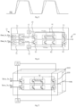
- Figure 3 is a schematic diagram of output signals DQ of the signal output terminal 60 prior to and after compensation.
- the solid line is the output signal after compensation
- the dashed line is the output signal prior to compensation.
- the pull-up compensation unit 51 is turned on on the rising edge of the output signal
- the pull-down compensation unit 52 is turned on on the falling edge of the output signal. The slew rate of the rising edge and the falling edge of the output signal after compensation increases compared to that prior to compensation.
- the output driving circuit further includes at least one delay unit (not shown in the drawings), the delay unit is arranged at the input terminal of the pulse signal generation circuit, and the positive input signal Data_In_Pos or the negative input signal Data_In_Neg is inputted to the pulse signal generation circuit through the delay unit, to adjust a compensation size of the compensation unit, which can further control the slew rate of the output signal DQ.
- the delay unit may be implemented through RC delay or by series connection with an inverter-based delay unit.
- a compensation current of the compensation unit be changed by adjusting the pulse width of the pulse signal and then adjusting an ON time of the compensation unit by the pulse signal generation circuit, but also the magnitude of the compensation current of the compensation unit can be adjusted by adjusting the number and size of transistors included in the compensation unit.
- the output driving circuit further includes a pull-up impedance calibration unit 81 and a pull-down impedance calibration unit 82.
- An input signal of the pull-up impedance calibration unit 81 is ZQ_PU ⁇ m>
- an input signal of the pull-down impedance calibration unit 82 is ZQ_PD ⁇ m>.
- the pull-up impedance calibration unit 81 is connected in parallel with the pull-up output unit 20, and the pull-down impedance calibration unit 82 is connected in parallel with the pull-down output unit 30, so as to calibrate the pull-up output unit 20 and the pull-down output unit 30.
- the pull-up impedance calibration unit 81 may be formed by a plurality of transistors connected in parallel.
- the pull-down impedance calibration unit 82 may also be formed by a plurality of transistors connected in parallel.
- the present application further provides another embodiment of an output driving circuit.
- Figure 4 is a schematic diagram of a second embodiment of the output driving circuit according to the present application.
- the second embodiment is different from the first embodiment in that the output driving circuit further includes a pull-up pre-amplification unit 71 and a pull-down pre-amplification unit 72.
- the pull-up pre-amplification unit 71 includes a first terminal and a second terminal.
- the first terminal is connected to the positive input signal Data_In_Pos
- the second terminal is connected to the control terminal of the pull-up output unit 20.
- the second terminal may also be connected to the input terminal of the pulse signal generation circuit.
- the second terminal is connected to the pull-up pulse signal generation circuit 41.
- An output signal PU_Main generated by the pull-up pre-amplification unit 71 acts as input signals of the pull-up output unit 20 and the pull-up pulse signal generation circuit 41.
- the pull-down pre-amplification unit 72 includes a first terminal and a second terminal.
- the first terminal is connected to the negative input signal Data_In_Neg, and the second terminal is connected to the control terminal of the pull-down output unit 30.
- the second terminal may also be connected to the input terminal of the pulse signal generation circuit.
- the second terminal is connected to the pull-down pulse signal generation circuit 42.
- An output signal PD_Main generated by the pull-down pre-amplification unit 72 acts as input signals of the pull-down output unit 30 and the pull-down pulse signal generation circuit 42.
- FIG. 5 is a schematic diagram of a third embodiment of the output driving circuit according to the present application.
- the output driving circuit includes a plurality of driving modules 100.
- the driving modules 100 are arranged in parallel, and the driving modules 100 have the same layout.
- the driving modules 100 are multiplexed, which can greatly simplify the design of the circuit and the realization of the layout, improve a degree of matching between the driving modules, and reduce the parasitism between the circuits, especially high-speed signal lines, so as to improve the performance of the circuit under high-speed operation.
- the driving module 100 includes at least the signal input terminal 10, the pull-up output unit 20, the pull-down output unit 30, the compensation unit and the signal input terminal 10.
- the pulse signal generation circuit may act as part of the output driving circuit, or the plurality of driving modules 100 can share the same pulse signal generating circuit. In this embodiment, the plurality of driving modules 100 share the same pulse signal generating circuit, so as to save power consumption. Further, the driving module 100 may also include a pull-up pre-amplification unit 71 and a pull-down pre-amplification unit 72.
- the signal input terminal 10, the pull-up output unit 20, the pull-down output unit 30, the compensation unit, the pulse signal generation circuit, the pull-up pre-amplification unit 71 and the pull-down pre-amplification unit 72 are the same as those described above, and are not described in detail.
- the present application further provides a memory including the output driving circuit as described above.
- the memory includes, but is not limited to, a DDR4, an LPDDR4, an LPDDR4X, an LPDDR5 and other DRAMs in need of high-speed data transmission.
Landscapes
- Engineering & Computer Science (AREA)
- Computer Hardware Design (AREA)
- Physics & Mathematics (AREA)
- Computing Systems (AREA)
- General Engineering & Computer Science (AREA)
- Mathematical Physics (AREA)
- Databases & Information Systems (AREA)
- Microelectronics & Electronic Packaging (AREA)
- Logic Circuits (AREA)
- Dram (AREA)
Applications Claiming Priority (2)
| Application Number | Priority Date | Filing Date | Title |
|---|---|---|---|
| CN202010207543.6A CN113437962A (zh) | 2020-03-23 | 2020-03-23 | 输出驱动电路及存储器 |
| PCT/CN2021/075940 WO2021190190A1 (zh) | 2020-03-23 | 2021-02-08 | 输出驱动电路及存储器 |
Publications (2)
| Publication Number | Publication Date |
|---|---|
| EP4131783A1 true EP4131783A1 (de) | 2023-02-08 |
| EP4131783A4 EP4131783A4 (de) | 2023-09-06 |
Family
ID=77752490
Family Applications (1)
| Application Number | Title | Priority Date | Filing Date |
|---|---|---|---|
| EP21773281.7A Withdrawn EP4131783A4 (de) | 2020-03-23 | 2021-02-08 | Ausgangstreiberschaltung und speicher |
Country Status (4)
| Country | Link |
|---|---|
| US (1) | US11870437B2 (de) |
| EP (1) | EP4131783A4 (de) |
| CN (1) | CN113437962A (de) |
| WO (1) | WO2021190190A1 (de) |
Cited By (1)
| Publication number | Priority date | Publication date | Assignee | Title |
|---|---|---|---|---|
| EP4195509A4 (de) * | 2020-08-07 | 2024-07-31 | Changxin Memory Technologies, Inc. | Treiberschaltung |
Families Citing this family (3)
| Publication number | Priority date | Publication date | Assignee | Title |
|---|---|---|---|---|
| CN117198355A (zh) * | 2022-05-30 | 2023-12-08 | 长鑫存储技术有限公司 | 半导体器件和存储器 |
| US20250112717A1 (en) * | 2023-09-29 | 2025-04-03 | Qualcomm Incorporated | Signal transmitter circuit including main full unit interval (ui) transmit driver and mid-sub-ui boost driver |
| CN117497020B (zh) * | 2023-12-29 | 2024-04-19 | 长鑫存储技术(西安)有限公司 | 输出驱动电路及存储器 |
Family Cites Families (16)
| Publication number | Priority date | Publication date | Assignee | Title |
|---|---|---|---|---|
| US5128555A (en) * | 1991-03-18 | 1992-07-07 | Motorola, Inc. | Pulsed CMOS logic circuit having selectable rise and fall times |
| JP3033523B2 (ja) * | 1997-05-16 | 2000-04-17 | 日本電気株式会社 | 出力回路 |
| JPH10326489A (ja) * | 1997-05-26 | 1998-12-08 | Mitsubishi Electric Corp | 半導体集積回路装置 |
| US6091260A (en) * | 1998-11-13 | 2000-07-18 | Integrated Device Technology, Inc. | Integrated circuit output buffers having low propagation delay and improved noise characteristics |
| JP3667690B2 (ja) * | 2001-12-19 | 2005-07-06 | エルピーダメモリ株式会社 | 出力バッファ回路及び半導体集積回路装置 |
| KR20050003895A (ko) * | 2003-07-04 | 2005-01-12 | 삼성전자주식회사 | 풀업 슬루율을 용이하게 조절할 수 있는 오픈 드레인출력버퍼 회로 |
| US7265585B2 (en) * | 2004-12-14 | 2007-09-04 | Infineon Technologies Ag | Method to improve current and slew rate ratio of off-chip drivers |
| KR100879747B1 (ko) * | 2006-06-30 | 2009-01-21 | 주식회사 하이닉스반도체 | 데이터 입출력드라이버의 임피던스를 조정할 수 있는반도체 장치 |
| JP2011211608A (ja) * | 2010-03-30 | 2011-10-20 | Renesas Electronics Corp | インピーダンス調整回路及びその制御方法 |
| US8471602B2 (en) | 2010-04-30 | 2013-06-25 | SK Hynix Inc. | Output driver and semiconductor apparatus having the same |
| CN104834341B (zh) * | 2015-05-13 | 2016-07-06 | 灿芯半导体(上海)有限公司 | 一种接口电路中的输出阻抗调整电路 |
| KR102529968B1 (ko) * | 2016-05-11 | 2023-05-08 | 삼성전자주식회사 | 반도체 메모리 장치의 임피던스 조정 회로, 반도체 메모리 장치 및 반도체 메모리 장치의 동작 방법 |
| CN107919154B (zh) * | 2017-12-11 | 2018-10-26 | 长鑫存储技术有限公司 | 一种输入输出驱动器校准电路、方法及半导体存储器 |
| US10756737B1 (en) * | 2019-09-24 | 2020-08-25 | Nanya Technology Corporation | Off chip driver circuit, off chip driver compensation system and signal compensation method |
| CN211744448U (zh) * | 2020-03-23 | 2020-10-23 | 长鑫存储技术(上海)有限公司 | 输出驱动电路及存储器 |
| KR102763935B1 (ko) * | 2020-05-21 | 2025-02-07 | 에스케이하이닉스 주식회사 | 송신 회로 |
-
2020
- 2020-03-23 CN CN202010207543.6A patent/CN113437962A/zh active Pending
-
2021
- 2021-02-08 WO PCT/CN2021/075940 patent/WO2021190190A1/zh not_active Ceased
- 2021-02-08 EP EP21773281.7A patent/EP4131783A4/de not_active Withdrawn
- 2021-02-08 US US17/595,717 patent/US11870437B2/en active Active
Cited By (1)
| Publication number | Priority date | Publication date | Assignee | Title |
|---|---|---|---|---|
| EP4195509A4 (de) * | 2020-08-07 | 2024-07-31 | Changxin Memory Technologies, Inc. | Treiberschaltung |
Also Published As
| Publication number | Publication date |
|---|---|
| US11870437B2 (en) | 2024-01-09 |
| CN113437962A (zh) | 2021-09-24 |
| EP4131783A4 (de) | 2023-09-06 |
| WO2021190190A1 (zh) | 2021-09-30 |
| US20220255548A1 (en) | 2022-08-11 |
Similar Documents
| Publication | Publication Date | Title |
|---|---|---|
| US11870437B2 (en) | Output driving circuit and memory | |
| US6339344B1 (en) | Semiconductor integrated circuit device | |
| US8674720B2 (en) | Semiconductor device and method of adjusting an impedance of an output buffer | |
| US20110279159A1 (en) | Circuits and methods for clock signal duty-cycle correction | |
| KR100656470B1 (ko) | 반도체 메모리의 드라이버 제어장치 및 방법 | |
| US20150071013A1 (en) | Semiconductor Device Having Level Shift Circuit | |
| US11790983B2 (en) | Output drive circuit and memory device | |
| CN210606642U (zh) | 输出驱动电路及存储器 | |
| US10585835B1 (en) | Methods and apparatuses for independent tuning of on-die termination impedances and output driver impedances, and related semiconductor devices and systems | |
| US10658020B2 (en) | Strobe signal generation circuit and semiconductor apparatus including the same | |
| US6952370B2 (en) | Data output buffer capable of controlling data valid window in semiconductor memory devices | |
| US9153312B2 (en) | Methods and apparatuses including transmitter circuits | |
| US20250141434A1 (en) | Methods and circuits for slew-rate calibration | |
| US7688645B2 (en) | Output circuit for a semiconductor memory device and data output method | |
| US8856577B2 (en) | Semiconductor device having multiplexer | |
| US7498844B2 (en) | Output driver for dynamic random access memory | |
| CN211744448U (zh) | 输出驱动电路及存储器 | |
| US12556186B2 (en) | Clock multiplexing circuit, clock distribution circuit, and semiconductor apparatus including the clock multiplexing circuit | |
| US11705898B2 (en) | Off chip driver circuit, off chip driver system, and method for manufacturing an off chip driver circuit | |
| KR100776740B1 (ko) | 반도체 메모리의 데이터 출력장치 및 방법 | |
| US12288582B2 (en) | Semiconductor memory device and method for compensating slew rate using impedance calibration | |
| CN110827885B (zh) | 输入接收器电路及自适应反馈方法 | |
| US11955166B2 (en) | Apparatuses and methods for signal transmission preconditioning | |
| US12499928B2 (en) | Memory system and receiver | |
| KR100607168B1 (ko) | 1/2 전원전압 발생회로 및 이를 이용한 반도체 메모리 장치 |
Legal Events
| Date | Code | Title | Description |
|---|---|---|---|
| STAA | Information on the status of an ep patent application or granted ep patent |
Free format text: STATUS: UNKNOWN |
|
| STAA | Information on the status of an ep patent application or granted ep patent |
Free format text: STATUS: THE INTERNATIONAL PUBLICATION HAS BEEN MADE |
|
| PUAI | Public reference made under article 153(3) epc to a published international application that has entered the european phase |
Free format text: ORIGINAL CODE: 0009012 |
|
| STAA | Information on the status of an ep patent application or granted ep patent |
Free format text: STATUS: REQUEST FOR EXAMINATION WAS MADE |
|
| 17P | Request for examination filed |
Effective date: 20210929 |
|
| AK | Designated contracting states |
Kind code of ref document: A1 Designated state(s): AL AT BE BG CH CY CZ DE DK EE ES FI FR GB GR HR HU IE IS IT LI LT LU LV MC MK MT NL NO PL PT RO RS SE SI SK SM TR |
|
| DAV | Request for validation of the european patent (deleted) | ||
| DAX | Request for extension of the european patent (deleted) | ||
| A4 | Supplementary search report drawn up and despatched |
Effective date: 20230809 |
|
| RIC1 | Information provided on ipc code assigned before grant |
Ipc: H03K 19/017 20060101ALI20230803BHEP Ipc: H03K 19/0185 20060101ALI20230803BHEP Ipc: H03K 19/0175 20060101AFI20230803BHEP |
|
| STAA | Information on the status of an ep patent application or granted ep patent |
Free format text: STATUS: THE APPLICATION IS DEEMED TO BE WITHDRAWN |
|
| 18D | Application deemed to be withdrawn |
Effective date: 20240312 |