EP4131940A1 - Élément d'imagerie à semi-conducteur et système d'imagerie - Google Patents
Élément d'imagerie à semi-conducteur et système d'imagerie Download PDFInfo
- Publication number
- EP4131940A1 EP4131940A1 EP21775284.9A EP21775284A EP4131940A1 EP 4131940 A1 EP4131940 A1 EP 4131940A1 EP 21775284 A EP21775284 A EP 21775284A EP 4131940 A1 EP4131940 A1 EP 4131940A1
- Authority
- EP
- European Patent Office
- Prior art keywords
- semiconductor
- carrier
- solid
- charge carriers
- state image
- Prior art date
- Legal status (The legal status is an assumption and is not a legal conclusion. Google has not performed a legal analysis and makes no representation as to the accuracy of the status listed.)
- Granted
Links
Images



Classifications
-
- H—ELECTRICITY
- H04—ELECTRIC COMMUNICATION TECHNIQUE
- H04N—PICTORIAL COMMUNICATION, e.g. TELEVISION
- H04N25/00—Circuitry of solid-state image sensors [SSIS]; Control thereof
- H04N25/70—SSIS architectures; Circuits associated therewith
- H04N25/79—Arrangements of circuitry being divided between different or multiple substrates, chips or circuit boards, e.g. stacked image sensors
-
- H—ELECTRICITY
- H04—ELECTRIC COMMUNICATION TECHNIQUE
- H04N—PICTORIAL COMMUNICATION, e.g. TELEVISION
- H04N25/00—Circuitry of solid-state image sensors [SSIS]; Control thereof
- H04N25/60—Noise processing, e.g. detecting, correcting, reducing or removing noise
-
- H—ELECTRICITY
- H04—ELECTRIC COMMUNICATION TECHNIQUE
- H04N—PICTORIAL COMMUNICATION, e.g. TELEVISION
- H04N25/00—Circuitry of solid-state image sensors [SSIS]; Control thereof
- H04N25/60—Noise processing, e.g. detecting, correcting, reducing or removing noise
- H04N25/62—Detection or reduction of noise due to excess charges produced by the exposure, e.g. smear, blooming, ghost image, crosstalk or leakage between pixels
-
- H—ELECTRICITY
- H04—ELECTRIC COMMUNICATION TECHNIQUE
- H04N—PICTORIAL COMMUNICATION, e.g. TELEVISION
- H04N25/00—Circuitry of solid-state image sensors [SSIS]; Control thereof
- H04N25/70—SSIS architectures; Circuits associated therewith
- H04N25/76—Addressed sensors, e.g. MOS or CMOS sensors
- H04N25/77—Pixel circuitry, e.g. memories, A/D converters, pixel amplifiers, shared circuits or shared components
- H04N25/771—Pixel circuitry, e.g. memories, A/D converters, pixel amplifiers, shared circuits or shared components comprising storage means other than floating diffusion
-
- H—ELECTRICITY
- H10—SEMICONDUCTOR DEVICES; ELECTRIC SOLID-STATE DEVICES NOT OTHERWISE PROVIDED FOR
- H10F—INORGANIC SEMICONDUCTOR DEVICES SENSITIVE TO INFRARED RADIATION, LIGHT, ELECTROMAGNETIC RADIATION OF SHORTER WAVELENGTH OR CORPUSCULAR RADIATION
- H10F39/00—Integrated devices, or assemblies of multiple devices, comprising at least one element covered by group H10F30/00, e.g. radiation detectors comprising photodiode arrays
- H10F39/80—Constructional details of image sensors
- H10F39/803—Pixels having integrated switching, control, storage or amplification elements
- H10F39/8037—Pixels having integrated switching, control, storage or amplification elements the integrated elements comprising a transistor
-
- H—ELECTRICITY
- H10—SEMICONDUCTOR DEVICES; ELECTRIC SOLID-STATE DEVICES NOT OTHERWISE PROVIDED FOR
- H10F—INORGANIC SEMICONDUCTOR DEVICES SENSITIVE TO INFRARED RADIATION, LIGHT, ELECTROMAGNETIC RADIATION OF SHORTER WAVELENGTH OR CORPUSCULAR RADIATION
- H10F39/00—Integrated devices, or assemblies of multiple devices, comprising at least one element covered by group H10F30/00, e.g. radiation detectors comprising photodiode arrays
- H10F39/80—Constructional details of image sensors
- H10F39/809—Constructional details of image sensors of hybrid image sensors
-
- H—ELECTRICITY
- H10—SEMICONDUCTOR DEVICES; ELECTRIC SOLID-STATE DEVICES NOT OTHERWISE PROVIDED FOR
- H10F—INORGANIC SEMICONDUCTOR DEVICES SENSITIVE TO INFRARED RADIATION, LIGHT, ELECTROMAGNETIC RADIATION OF SHORTER WAVELENGTH OR CORPUSCULAR RADIATION
- H10F39/00—Integrated devices, or assemblies of multiple devices, comprising at least one element covered by group H10F30/00, e.g. radiation detectors comprising photodiode arrays
- H10F39/10—Integrated devices
- H10F39/12—Image sensors
- H10F39/18—Complementary metal-oxide-semiconductor [CMOS] image sensors; Photodiode array image sensors
- H10F39/184—Infrared image sensors
-
- Y—GENERAL TAGGING OF NEW TECHNOLOGICAL DEVELOPMENTS; GENERAL TAGGING OF CROSS-SECTIONAL TECHNOLOGIES SPANNING OVER SEVERAL SECTIONS OF THE IPC; TECHNICAL SUBJECTS COVERED BY FORMER USPC CROSS-REFERENCE ART COLLECTIONS [XRACs] AND DIGESTS
- Y02—TECHNOLOGIES OR APPLICATIONS FOR MITIGATION OR ADAPTATION AGAINST CLIMATE CHANGE
- Y02E—REDUCTION OF GREENHOUSE GAS [GHG] EMISSIONS, RELATED TO ENERGY GENERATION, TRANSMISSION OR DISTRIBUTION
- Y02E10/00—Energy generation through renewable energy sources
- Y02E10/50—Photovoltaic [PV] energy
- Y02E10/547—Monocrystalline silicon PV cells
Definitions
- the present invention relates to solid-state image sensors and imaging systems.
- Solid-state imaging devices are used in various fields. As one example, solid-state imaging devices are used in imaging systems that can measure distances to objects.
- imaging systems typically include a light source for producing light to be emitted toward an object, and a solid-state imaging device.
- the imaging device functions as an image sensor that captures an image of light reflected from the object.
- One issue with the above imaging device is noise due to external light.
- One measure which has been considered to reduce this noise is to use near-infrared or short-wave infrared light at wavelengths that sunlight contains little of (preferably, light at wavelengths of about 1350 nm to 1400 nm that sunlight contains little of). This allows the above imaging device to be substantially unaffected by many types of external light, including sunlight.
- germanium (Ge) and the like having a high absorption coefficient have been considered for use.
- PTL 1 discloses a device having photodiodes formed in a layer containing Ge and silicon (Si).
- the device disclosed in PTL 1 includes a first semiconductor with photodiodes formed therein, and a second semiconductor disposed on a silicon substrate. Although charge carriers generated by the photodiodes in the first semiconductor are transferred to the second semiconductor for subsequent carrier-to-voltage conversion, PTL 1 does not specifically describe the manner in which the charge carriers are transferred from the first semiconductor to the second semiconductor, but it only illustrates, by way of example, a known interconnection using conductive wiring and a diffusion layer.
- charge carriers generated in a photodiode may be subjected to selective transfer to one of a plurality of carrier-storage regions.
- PTL 1 discloses a time-of-flight (ToF) optical sensor in which charge carriers transferred to a second semiconductor are subjected to selective transfer to one of two carrier-storage regions.
- ToF time-of-flight
- the present invention aims to provide a solid-state image sensor that efficiently uses near-infrared or short-wave infrared light and that performs appropriate selective carrier transfer.
- a solid-state image sensor includes a first semiconductor having a first composition, and a second semiconductor having a second composition different from the first composition and electrically connected to the first semiconductor.
- the first semiconductor includes a photodiode configured to convert light incident on the photodiode into charge carriers; a plurality of first carrier storages for storing the charge carriers; and a transfer controller configured to transfer the charge carriers to a selected one of the first carrier storages.
- the second semiconductor includes a plurality of second carrier storages and a potential detector.
- the second carrier storages correspond to the respective first carrier storages and are each configured to store charge carriers based on the charge carriers stored in a corresponding one of the first carrier storages.
- the potential detector is configured to detect the electric potential of each of the second carrier storages.
- the solid-state image sensor further includes a resetter configured to reset the electric potential of each of the first carrier storages to a predetermined electric potential.
- An imaging system includes a light source unit configured to emit light having a predetermined wavelength profile; and a solid-state image sensor according to the first aspect.
- the above aspects of the present invention enable efficient use of near-infrared or short-wave infrared light and appropriate selective carrier transfer.
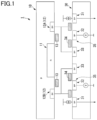
- Fig. 1 is a schematic diagram illustrating the configuration of a solid-state image sensor 1 according to the present embodiment.
- the solid-state image sensor 1 includes a first semiconductor 10 and a second semiconductor 30 electrically connected to each other.
- the first semiconductor 10 and the second semiconductor 30 have different compositions of constituent elements and different lattice constants.
- the first semiconductor 10 includes a known photodiode (PD) 11 and thus is configured to perform photoelectric conversion from incident light into signal charge carriers and to store the signal charge carriers.
- the photodiode 11 may be omitted depending, for example, on the concentration of impurities in the first semiconductor 10. In the present case, the geometric region of the first semiconductor 10 occupied by the photodiode 11 has a function of performing the photoelectric conversion.
- At least the portion of the first semiconductor 10 occupied by the photodiode 11 is composed of a high proportion of elements or compounds that are excellent in properties of absorbing near-infrared or short-wave infrared light, in particular light in a wavelength range from about 1350 nm to 1400 nm.
- a typical example of such a material is Ge, and other examples thereof include germanium compounds, such as germanium-silicon (GeSi), and gallium antimonide (GaSb). In the following description, these materials may be collectively referred to as "Ge or the like".
- the physical structure of the first semiconductor 10 is not particularly limited.
- the entire first semiconductor 10 may be composed of Ge alone or a mixed crystal including Ge or the like.
- the first semiconductor 10 may include layers of Ge or the like alternating with layers of another material, such as silicon or the like.
- first semiconductor 10 is of a p-type
- first semiconductor 10 is of an n-type
- a p-type semiconductor may be indicated with "p”.
- an n-type semiconductor may be indicated with "n”
- a p+ semiconductor region may be indicated with "p+”
- an n+ semiconductor region may be indicated with "n+”.
- the first semiconductor 10 includes a plurality of first carrier storages 12. Each first carrier storage 12 of the present embodiment may be, for example, an n+ semiconductor region.
- the first semiconductor 10 includes two first carrier storages 12, namely a first carrier storage 12A and a first carrier storage 12B.
- the first semiconductor 10 includes first and second transfer gates (transfer controllers) 13 each disposed between the photodiode 11 and a corresponding one of the first carrier storages 12A and 12B.
- the first and second transfer gates (transfer controllers) 13 each transfer charge carriers generated by the photoelectric conversion to a corresponding one of the first carrier storages 12A and 12B.
- the transfer gates 13 each have a known structure, for example, a metal-oxide-semiconductor (MOS) structure.
- MOS metal-oxide-semiconductor
- the second semiconductor 30 is a semiconductor provided primarily for signal processing and may be composed of silicon.
- the second semiconductor 30 is electrically connected to the first semiconductor 10 by interconnection through diffusion layers.
- the second semiconductor 30 includes second carrier storages 33, drains 32 of respective reset transistors (resetters) 35, potential detection nodes (potential detectors) 31, and reset gates 34 of the respective reset transistors (resetters) 35.
- Each second carrier storage 33 is connected to a readout circuit (not illustrated).
- Each potential detection node (potential detector) 31 detects the electric potential of a corresponding one of the second carrier storages 33.
- Each reset gate 34 controls the transfer of charge carriers between one of the second carrier storages 33 and the corresponding drain 32.
- Each reset transistor (resetter) 35 is configured to reset the electric potential of a corresponding one of the first carrier storages 12 to a predetermined electric potential.
- Each reset transistor 35 may be, for example, a field-effect-transistor (FET).
- Each second carrier storage 33, drain 32, potential detection node 31, and reset gate 34 is provided for a corresponding one of the first carrier storages 12A and 12B.
- Each potential detection node 31 is configured to detect the electric potential of a corresponding one of the second carrier storages 33.
- each transfer gate 13 causes charge carriers generated in the photodiode 11 to be transferred to one of the first carrier storages 12A and 12B.
- a control signal is applied to each transfer gate 13 so as to change with time the destination to which charge carriers generated in the photodiode 11 are transferred; thus, selective carrier transfer is performed.
- charge carriers generated in the photodiode 11 are subjected to selective transfer to one of the first carrier storages 12A and 12B in the first semiconductor 10.
- the generated charge carriers are transferred to the first carrier storage 12A and the corresponding second carrier storage 33, which are diffusion layers serving as capacitors, and to a capacitor composed of a first gate electrode disposed in the second semiconductor 30 and a line (not illustrated) connecting the first carrier storage 12A to the corresponding second carrier storage 33.
- the generated charge carriers are transferred to the first carrier storage 12B and the corresponding second carrier storage 33, which are diffusion layers serving as capacitors, and to a capacitor composed of a second gate electrode disposed in the second semiconductor 30 and a line (not illustrated) connecting the first carrier storage 12B to the corresponding second carrier storage 33. Accordingly, the charge carriers transferred to be stored in the capacitors will not be subjected to selective transfer.
- the solid-state image sensor 1 of the present embodiment is configured to perform selective transfer of charge carriers in the first semiconductor 10. This configuration does not involve transfer of charge carriers from a large-capacitance capacitor, thus achieving appropriate selective transfer of charge carriers.
- the solid-state image sensor 1 of the present embodiment includes the first semiconductor 10 having the transfer gates 13 as transfer controllers and the first carrier storages 12 as transfer destinations. With this configuration, appropriate selective carrier transfer can be achieved in the solid-state image sensor 1 with a heterojunction between the first and second semiconductors 10 and 30, which are different semiconductors.
- the photodiode 11 of the first semiconductor 10 is composed of Ge or the like as its main material. With this configuration, it can be said that the solid-state image sensor 1 is capable of operating appropriately as a multi-gate ToF sensor that uses near-infrared or short-wave infrared light, in particular light in a wavelength range from about 1350 nm to 1400 nm.
- the number of the first carrier storages may be set as appropriate. That is, although the first semiconductor has been described as having the two first carrier storages by way of example, three or more first carrier storages may be provided therein.
- Fig. 2 is a schematic diagram illustrating a solid-state image sensor 1A according to a modification of the present embodiment.
- the transfer gates 13 are replaced by a first p+ semiconductor region 15 disposed between the photodiode 11 and the first carrier storage 12A and a second p+ semiconductor region 15 disposed between the photodiode 11 and the first carrier storage 12B.
- Each p+ semiconductor region 15 is connected to a voltage signal generator 16.
- Charge carriers generated in the photodiode 11 are transferred to one of the first carrier storages 12A and 12B in response to each p+ semiconductor region 15 receiving a signal from the voltage signal generator 16.
- the transfer controller 17 of the solid-state image sensor 1A includes the first and second p+ semiconductor regions 15 and the voltage signal generator 16 and performs selective carrier transfer using a known current assisted technique.
- the transfer controller configured as such also achieves the effect described above, and thus the transfer controller is not limited to a gate electrode.
- FIG. 2 illustrates the first and second p+ semiconductor regions 15 each disposed between the photodiode 11 and the corresponding first carrier storage 12, these p+ semiconductor regions 15 may be disposed at any position as long as they are in the vicinity of the respective first carrier storages 12A and 12B.
- Fig. 2 illustrates a front-side illumination (FSI) solid-state image sensor where the first semiconductor 10 has the photodiode 11 formed on the side facing away from the second semiconductor.
- All the solid-state image sensors described in the present specification may have an FSI configuration or a back-side illumination (BSI) configuration, depending, for example, on the use and/or the relation with other configurations.
- FSI front-side illumination
- BSI back-side illumination
- solid-state image sensor of the present embodiment can be used singly, but in another possible configuration, solid-state image sensors of the present embodiment may be arranged in a two-dimensional matrix to provide a solid-state imaging device having a plurality of pixels.
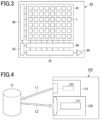
- Fig. 3 is a block diagram illustrating an example of such an imaging device.
- the solid-state imaging device 40 includes a light receiving region 41 in which a two-dimensional array of solid-state image sensors 1 is disposed.
- the solid-state imaging device 40 is illustrated as including, by way of example, a control circuit 50, a vertical driving circuit 60, a horizontal driving circuit 70, an analog-to-digital (AD) conversion circuit 80, and an output circuit 90.
- the solid-state imaging device 40 may include known various components suitably combined considering, for example, specifications.
- the number and arrangement of solid-state image sensors disposed in the light receiving region 41 may be set as appropriate.
- the solid-state image sensors may be disposed in a two-dimensional array with no clearance therebetween. In this case, a two-dimensional array of solid-state image sensors may be formed on a single semiconductor wafer.
- Fig. 4 schematically illustrates an example of an imaging system in which the solid-state image sensor of the present embodiment is used.
- the imaging system 100 of Fig. 4 includes a light source unit 110 having a light source 101, and a light receiving unit 120 having an image sensor 121.
- the light source unit 110 includes the light source 101 and, if necessary, a filter, for example, that regulates the wavelength of light emitted from the light source 101.
- the light source unit 110 is configured to emit, to an object O, outgoing light L1 having a predetermined wavelength in a predetermined wavelength range (wavelength profile).
- the outgoing light L1 may be near-infrared or short-wave infrared light (e.g., light in a wavelength range from about 1350 nm to 1400 nm).
- the outgoing light L1 will be reflected by the object O as reflected light L2, and the reflected light L2 will be incident on the image sensor 121 of the light receiving unit 120.
- the image sensor 121 may be composed of one or more solid-state image sensors of the present embodiment.
- the imaging system 100 can, for example, measure distances to objects using a ToF technique while being substantially unaffected by external light even when used outdoors.
- the first semiconductor 10 may be provided with the drains 32 and reset gates 34 of the respective reset transistors 35.
- the first semiconductor 10 is capacitively coupled to the second semiconductor 30 via high-resistance gate electrodes, charge carriers subjected to selective transfer will move within the first semiconductor 10.
- This configuration provides a high degree of freedom in setting, for example, a reset voltage, and prevents contamination of charge carriers with noise through the respective second carrier storages 33, which are diffusion layers, to thereby achieve improved characteristics.
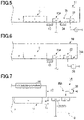
- the configuration of the reset transistor is not limited to the example illustrated in Fig. 5 .
- Reset transistors (resetters) 35A of the modification illustrated in Fig. 6 include respective voltage signal generators 36, with the reset gates 34 omitted.
- a voltage applied to a drain 32 will increase in response to a signal from the corresponding voltage signal generator 36, resulting in a depletion layer adjacent the drain 32 being coupled to a depletion layer of the corresponding first carrier storage 12A. Consequently, the electric potential of the first carrier storage 12A is set to a characteristic voltage determined by the electric potential distribution of a coupled depletion layer. That is, the first carrier storage 12A can be reset.
- the electric potential of the first carrier storage can be reset without a FET gate, such as the reset gate 34.
- the concentration of impurities may be different between each first carrier storage and the corresponding drain 32.
- a suitable impurity region may be disposed between each first carrier storage and the corresponding drain 32.
- Fig. 7 illustrates a modification where the solid-state image sensor 1A includes the reset transistors 35A.
- the solid-state image sensor 1A of Fig. 7 includes a transfer controller 17 and thus is configured to perform selective carrier transfer in response to external voltages.
- the first semiconductor 10 includes no FET gates when the reset transistors 35A are provided.
- the manufacturing process can be greatly simplified, resulting in a significant reduction in the manufacturing cost.
- Fig. 8 illustrates a modification where the first semiconductor 10 of the present embodiment includes drain structures 38 each configured to cause signal charge carriers (electrons in the case of a p-type first semiconductor 10) to discharge.
- the drain structures 38 each include a voltage signal generator 39.
- Unwanted charge carriers in the first carrier storage 12A are discharged into the corresponding drain structure 38 upon application of a reverse-bias voltage to the drain structure 38 from the corresponding voltage signal generator 39 to cause a reverse-bias condition relative to the first semiconductor 10.
- unwanted charge carriers are removed in advance, which improves a signal-to-noise (S/N) ratio of a signal for selective carrier transfer.
- S/N signal-to-noise
- Fig. 9 illustrates a solid-state image sensor 1A including drain structures 38.
- the first semiconductor 10 needs no FET gates.
- each of the drain structures 38 may be combined with the reset transistor 35A.
- each drain structure 38 and the corresponding reset transistor 35A may share part of their structure.
- a carrier discharger 18 coupled to the photodiode 11 via a gate may be provided in the first semiconductor 10.
- charge carriers generated in the photodiode 11 due to incident light or a dark current can be suitably discharged.
- the other first carrier storage 12B and corresponding components of the second semiconductor 30 are omitted because they are difficult to illustrate in the same drawing sheet.
- Fig. 11 illustrates a modification of the solid-state image sensor 1B where the transfer gate 13 is replaced with a transfer controller 17 including a p+ semiconductor region 15 and a voltage signal generator 16, and the gate of the carrier discharger 18 is replaced with a p+ semiconductor region 18a and a voltage signal generator 18b.
- the first semiconductor 10 includes no FET gates, and thus the above advantage can be obtained.
- the carrier discharger 18 may be combined with a reset transistor or a drain structure.
Landscapes
- Engineering & Computer Science (AREA)
- Multimedia (AREA)
- Signal Processing (AREA)
- Solid State Image Pick-Up Elements (AREA)
- Transforming Light Signals Into Electric Signals (AREA)
Applications Claiming Priority (2)
| Application Number | Priority Date | Filing Date | Title |
|---|---|---|---|
| JP2020054149A JP7505221B2 (ja) | 2020-03-25 | 2020-03-25 | 固体撮像素子および撮像システム |
| PCT/JP2021/009537 WO2021193066A1 (fr) | 2020-03-25 | 2021-03-10 | Élément d'imagerie à semi-conducteur et système d'imagerie |
Publications (3)
| Publication Number | Publication Date |
|---|---|
| EP4131940A1 true EP4131940A1 (fr) | 2023-02-08 |
| EP4131940A4 EP4131940A4 (fr) | 2023-08-23 |
| EP4131940B1 EP4131940B1 (fr) | 2026-05-06 |
Family
ID=77891459
Family Applications (1)
| Application Number | Title | Priority Date | Filing Date |
|---|---|---|---|
| EP21775284.9A Active EP4131940B1 (fr) | 2020-03-25 | 2021-03-10 | Capteur d'image à état solide et système d'imagerie |
Country Status (6)
| Country | Link |
|---|---|
| US (1) | US12568698B2 (fr) |
| EP (1) | EP4131940B1 (fr) |
| JP (1) | JP7505221B2 (fr) |
| CN (1) | CN115336255B (fr) |
| TW (1) | TWI878502B (fr) |
| WO (1) | WO2021193066A1 (fr) |
Families Citing this family (4)
| Publication number | Priority date | Publication date | Assignee | Title |
|---|---|---|---|---|
| WO2024057470A1 (fr) * | 2022-09-15 | 2024-03-21 | ソニーセミコンダクタソリューションズ株式会社 | Dispositif de photodétection, son procédé de production et appareil électronique |
| US12417615B2 (en) | 2023-05-16 | 2025-09-16 | Bank Of America Corporation | System and method for consolidation of alerts and events using image matching of heatmap descriptions of infrastructure status |
| US12505003B2 (en) | 2023-05-17 | 2025-12-23 | Bank Of America Corporation | System and method for multi image matching for outage prediction, prevention, and mitigation for technology infrastructure using hybrid deep learning |
| US12373271B2 (en) | 2023-05-25 | 2025-07-29 | Bank Of America Corporation | System and method for matching multiple featureless images across a time series for outage prediction and prevention |
Family Cites Families (12)
| Publication number | Priority date | Publication date | Assignee | Title |
|---|---|---|---|---|
| JP2004304331A (ja) * | 2003-03-28 | 2004-10-28 | Matsushita Electric Ind Co Ltd | 固体撮像装置 |
| JP2008244021A (ja) * | 2007-03-26 | 2008-10-09 | Matsushita Electric Ind Co Ltd | 固体撮像装置およびそれを用いたカメラ |
| TWI723890B (zh) * | 2015-08-04 | 2021-04-01 | 光澄科技股份有限公司 | 製造影像感測陣列之方法 |
| WO2017022218A1 (fr) * | 2015-08-04 | 2017-02-09 | パナソニックIpマネジメント株式会社 | Dispositif d'imagerie à semi-conducteurs |
| CN113099137A (zh) * | 2015-09-30 | 2021-07-09 | 株式会社尼康 | 拍摄元件 |
| JP6706482B2 (ja) * | 2015-11-05 | 2020-06-10 | ソニーセミコンダクタソリューションズ株式会社 | 固体撮像装置および電子機器 |
| CN112929586B (zh) * | 2015-12-03 | 2024-12-06 | 松下知识产权经营株式会社 | 摄像装置 |
| WO2018191539A1 (fr) | 2017-04-13 | 2018-10-18 | Artilux Corporation | Appareil de détection de lumière à silicium-germanium |
| US10192911B2 (en) * | 2017-05-09 | 2019-01-29 | Apple Inc. | Hybrid image sensors with improved charge injection efficiency |
| TW202003938A (zh) * | 2018-05-18 | 2020-01-16 | 雁丞有限公司 | 疊紗與夾入織物 |
| JP2021176154A (ja) | 2018-07-18 | 2021-11-04 | ソニーセミコンダクタソリューションズ株式会社 | 受光素子および測距モジュール |
| JP2020054149A (ja) | 2018-09-27 | 2020-04-02 | 日本電産株式会社 | モータ |
-
2020
- 2020-03-25 JP JP2020054149A patent/JP7505221B2/ja active Active
-
2021
- 2021-03-10 WO PCT/JP2021/009537 patent/WO2021193066A1/fr not_active Ceased
- 2021-03-10 EP EP21775284.9A patent/EP4131940B1/fr active Active
- 2021-03-10 CN CN202180020789.5A patent/CN115336255B/zh active Active
- 2021-03-24 TW TW110110533A patent/TWI878502B/zh active
-
2022
- 2022-09-26 US US17/935,336 patent/US12568698B2/en active Active
Also Published As
| Publication number | Publication date |
|---|---|
| EP4131940A4 (fr) | 2023-08-23 |
| TW202141778A (zh) | 2021-11-01 |
| JP2021158418A (ja) | 2021-10-07 |
| WO2021193066A1 (fr) | 2021-09-30 |
| US12568698B2 (en) | 2026-03-03 |
| US20230014856A1 (en) | 2023-01-19 |
| TWI878502B (zh) | 2025-04-01 |
| JP7505221B2 (ja) | 2024-06-25 |
| CN115336255A (zh) | 2022-11-11 |
| EP4131940B1 (fr) | 2026-05-06 |
| CN115336255B (zh) | 2026-04-28 |
Similar Documents
| Publication | Publication Date | Title |
|---|---|---|
| EP4131940B1 (fr) | Capteur d'image à état solide et système d'imagerie | |
| JP7249548B2 (ja) | 撮像装置 | |
| US7453131B2 (en) | Photodiode detector and associated readout circuitry | |
| CN107004691B (zh) | 光检测装置 | |
| US10547016B2 (en) | Photoelectric conversion apparatus and imaging system | |
| KR102484157B1 (ko) | 변조된 이미지 캡처를 위한 시스템 및 방법 | |
| US10367029B2 (en) | Image sensors having a separation impurity layer | |
| US9401383B2 (en) | Photoconductive element for radiation detection in a radiography imaging system | |
| KR20170044007A (ko) | 솔라 셀 기능을 갖는 이미지 센서 | |
| CN113614931A (zh) | 光检测器 | |
| JP2018125839A (ja) | 撮像装置の制御方法及び撮像装置 | |
| EP2981069B1 (fr) | Appareil de conversion photoélectrique et système de conversion photoélectrique | |
| JP3655760B2 (ja) | 赤外線固体撮像素子 | |
| Kim et al. | Investigation of the global shutter operation of the quantum-dot short-wave infrared image sensor | |
| CN113016071A (zh) | 摄像装置 | |
| US11647641B2 (en) | Photo-sensitive device and a method for light detection in a photo-sensitive device | |
| WO2025214967A1 (fr) | Photodétecteur, capteur d'image et procédé de photodétection | |
| WO2025214971A1 (fr) | Photodétecteur, capteur d'image et procédé de photodétection | |
| CN121080142A (zh) | 具有可在光伏模式下操作的光电二极管的电磁辐射传感器器件 | |
| Abrahamian et al. | High-sensitive multielement line (matrixes) on the basis of field-effect transistors with easily reproduced production technology | |
| DURINI | formerly Fraunhofer Institute for Microelectronic Circuits and Systems |
Legal Events
| Date | Code | Title | Description |
|---|---|---|---|
| STAA | Information on the status of an ep patent application or granted ep patent |
Free format text: STATUS: THE INTERNATIONAL PUBLICATION HAS BEEN MADE |
|
| PUAI | Public reference made under article 153(3) epc to a published international application that has entered the european phase |
Free format text: ORIGINAL CODE: 0009012 |
|
| STAA | Information on the status of an ep patent application or granted ep patent |
Free format text: STATUS: REQUEST FOR EXAMINATION WAS MADE |
|
| 17P | Request for examination filed |
Effective date: 20220824 |
|
| AK | Designated contracting states |
Kind code of ref document: A1 Designated state(s): AL AT BE BG CH CY CZ DE DK EE ES FI FR GB GR HR HU IE IS IT LI LT LU LV MC MK MT NL NO PL PT RO RS SE SI SK SM TR |
|
| DAV | Request for validation of the european patent (deleted) | ||
| DAX | Request for extension of the european patent (deleted) | ||
| REG | Reference to a national code |
Ref country code: DE Ref legal event code: R079 Free format text: PREVIOUS MAIN CLASS: H04N0005374000 Ipc: H01L0027146000 Ref country code: DE Ref legal event code: R079 Ref document number: 602021053845 Country of ref document: DE Free format text: PREVIOUS MAIN CLASS: H04N0005374000 Ipc: H01L0027146000 |
|
| A4 | Supplementary search report drawn up and despatched |
Effective date: 20230726 |
|
| RIC1 | Information provided on ipc code assigned before grant |
Ipc: H04N 25/79 20230101ALI20230720BHEP Ipc: H01L 27/146 20060101AFI20230720BHEP |
|
| STAA | Information on the status of an ep patent application or granted ep patent |
Free format text: STATUS: EXAMINATION IS IN PROGRESS |
|
| 17Q | First examination report despatched |
Effective date: 20250512 |
|
| REG | Reference to a national code |
Ref country code: DE Ref legal event code: R079 Free format text: PREVIOUS MAIN CLASS: H01L0027146000 Ipc: H10F0039000000 Ref country code: DE Ref legal event code: R079 Ref document number: 602021053845 Country of ref document: DE Free format text: PREVIOUS MAIN CLASS: H01L0027146000 Ipc: H10F0039000000 |
|
| RIC1 | Information provided on ipc code assigned before grant |
Ipc: H10F 39/00 20250101AFI20251217BHEP Ipc: H04N 25/62 20230101ALI20251217BHEP Ipc: H04N 25/79 20230101ALI20251217BHEP Ipc: H04N 25/771 20230101ALI20251217BHEP |
|
| GRAP | Despatch of communication of intention to grant a patent |
Free format text: ORIGINAL CODE: EPIDOSNIGR1 |
|
| STAA | Information on the status of an ep patent application or granted ep patent |
Free format text: STATUS: GRANT OF PATENT IS INTENDED |
|
| INTG | Intention to grant announced |
Effective date: 20260127 |
|
| GRAS | Grant fee paid |
Free format text: ORIGINAL CODE: EPIDOSNIGR3 |
|
| GRAA | (expected) grant |
Free format text: ORIGINAL CODE: 0009210 |
|
| STAA | Information on the status of an ep patent application or granted ep patent |
Free format text: STATUS: THE PATENT HAS BEEN GRANTED |