EP4133317B1 - Verfahren zur herstellung einer mischschicht mit einem siliziumwellenleiter und einem siliziumnitridwellenleiter - Google Patents
Verfahren zur herstellung einer mischschicht mit einem siliziumwellenleiter und einem siliziumnitridwellenleiter Download PDFInfo
- Publication number
- EP4133317B1 EP4133317B1 EP21716431.8A EP21716431A EP4133317B1 EP 4133317 B1 EP4133317 B1 EP 4133317B1 EP 21716431 A EP21716431 A EP 21716431A EP 4133317 B1 EP4133317 B1 EP 4133317B1
- Authority
- EP
- European Patent Office
- Prior art keywords
- silicon
- waveguide
- core
- layer
- nitride
- Prior art date
- Legal status (The legal status is an assumption and is not a legal conclusion. Google has not performed a legal analysis and makes no representation as to the accuracy of the status listed.)
- Active
Links
Images


Classifications
-
- G—PHYSICS
- G02—OPTICS
- G02B—OPTICAL ELEMENTS, SYSTEMS OR APPARATUS
- G02B6/00—Light guides; Structural details of arrangements comprising light guides and other optical elements, e.g. couplings
- G02B6/10—Light guides; Structural details of arrangements comprising light guides and other optical elements, e.g. couplings of the optical waveguide type
- G02B6/12—Light guides; Structural details of arrangements comprising light guides and other optical elements, e.g. couplings of the optical waveguide type of the integrated circuit kind
- G02B6/13—Integrated optical circuits characterised by the manufacturing method
- G02B6/136—Integrated optical circuits characterised by the manufacturing method by etching
-
- H—ELECTRICITY
- H01—ELECTRIC ELEMENTS
- H01S—DEVICES USING THE PROCESS OF LIGHT AMPLIFICATION BY STIMULATED EMISSION OF RADIATION [LASER] TO AMPLIFY OR GENERATE LIGHT; DEVICES USING STIMULATED EMISSION OF ELECTROMAGNETIC RADIATION IN WAVE RANGES OTHER THAN OPTICAL
- H01S5/00—Semiconductor lasers
- H01S5/10—Construction or shape of the optical resonator, e.g. extended or external cavity, coupled cavities, bent-guide, varying width, thickness or composition of the active region
- H01S5/14—External cavity lasers
- H01S5/141—External cavity lasers using a wavelength selective device, e.g. a grating or etalon
- H01S5/142—External cavity lasers using a wavelength selective device, e.g. a grating or etalon which comprises an additional resonator
-
- G—PHYSICS
- G02—OPTICS
- G02B—OPTICAL ELEMENTS, SYSTEMS OR APPARATUS
- G02B6/00—Light guides; Structural details of arrangements comprising light guides and other optical elements, e.g. couplings
- G02B6/10—Light guides; Structural details of arrangements comprising light guides and other optical elements, e.g. couplings of the optical waveguide type
- G02B6/12—Light guides; Structural details of arrangements comprising light guides and other optical elements, e.g. couplings of the optical waveguide type of the integrated circuit kind
- G02B6/13—Integrated optical circuits characterised by the manufacturing method
- G02B6/132—Integrated optical circuits characterised by the manufacturing method by deposition of thin films
-
- H—ELECTRICITY
- H01—ELECTRIC ELEMENTS
- H01S—DEVICES USING THE PROCESS OF LIGHT AMPLIFICATION BY STIMULATED EMISSION OF RADIATION [LASER] TO AMPLIFY OR GENERATE LIGHT; DEVICES USING STIMULATED EMISSION OF ELECTROMAGNETIC RADIATION IN WAVE RANGES OTHER THAN OPTICAL
- H01S5/00—Semiconductor lasers
- H01S5/02—Structural details or components not essential to laser action
- H01S5/0206—Substrates, e.g. growth, shape, material, removal or bonding
- H01S5/021—Silicon based substrates
-
- H—ELECTRICITY
- H01—ELECTRIC ELEMENTS
- H01S—DEVICES USING THE PROCESS OF LIGHT AMPLIFICATION BY STIMULATED EMISSION OF RADIATION [LASER] TO AMPLIFY OR GENERATE LIGHT; DEVICES USING STIMULATED EMISSION OF ELECTROMAGNETIC RADIATION IN WAVE RANGES OTHER THAN OPTICAL
- H01S5/00—Semiconductor lasers
- H01S5/02—Structural details or components not essential to laser action
- H01S5/0206—Substrates, e.g. growth, shape, material, removal or bonding
- H01S5/0215—Bonding to the substrate
-
- H—ELECTRICITY
- H01—ELECTRIC ELEMENTS
- H01S—DEVICES USING THE PROCESS OF LIGHT AMPLIFICATION BY STIMULATED EMISSION OF RADIATION [LASER] TO AMPLIFY OR GENERATE LIGHT; DEVICES USING STIMULATED EMISSION OF ELECTROMAGNETIC RADIATION IN WAVE RANGES OTHER THAN OPTICAL
- H01S5/00—Semiconductor lasers
- H01S5/02—Structural details or components not essential to laser action
- H01S5/026—Monolithically integrated components, e.g. waveguides, monitoring photo-detectors, drivers
-
- H—ELECTRICITY
- H01—ELECTRIC ELEMENTS
- H01S—DEVICES USING THE PROCESS OF LIGHT AMPLIFICATION BY STIMULATED EMISSION OF RADIATION [LASER] TO AMPLIFY OR GENERATE LIGHT; DEVICES USING STIMULATED EMISSION OF ELECTROMAGNETIC RADIATION IN WAVE RANGES OTHER THAN OPTICAL
- H01S5/00—Semiconductor lasers
- H01S5/10—Construction or shape of the optical resonator, e.g. extended or external cavity, coupled cavities, bent-guide, varying width, thickness or composition of the active region
- H01S5/1028—Coupling to elements in the cavity, e.g. coupling to waveguides adjacent the active region, e.g. forward coupled [DFC] structures
- H01S5/1032—Coupling to elements comprising an optical axis that is not aligned with the optical axis of the active region
-
- G—PHYSICS
- G02—OPTICS
- G02B—OPTICAL ELEMENTS, SYSTEMS OR APPARATUS
- G02B6/00—Light guides; Structural details of arrangements comprising light guides and other optical elements, e.g. couplings
- G02B6/10—Light guides; Structural details of arrangements comprising light guides and other optical elements, e.g. couplings of the optical waveguide type
- G02B6/12—Light guides; Structural details of arrangements comprising light guides and other optical elements, e.g. couplings of the optical waveguide type of the integrated circuit kind
- G02B2006/12035—Materials
- G02B2006/12061—Silicon
-
- G—PHYSICS
- G02—OPTICS
- G02B—OPTICAL ELEMENTS, SYSTEMS OR APPARATUS
- G02B6/00—Light guides; Structural details of arrangements comprising light guides and other optical elements, e.g. couplings
- G02B6/10—Light guides; Structural details of arrangements comprising light guides and other optical elements, e.g. couplings of the optical waveguide type
- G02B6/14—Mode converters
Definitions
- silicon waveguide and silicon nitride waveguide designate waveguides whose cores are made, respectively, of silicon and silicon nitride.
- the three different waveguides are produced in respective layers stacked one above the other.
- the invention therefore aims to compensate for this lack. Its subject therefore is a process for manufacturing a mixed layer according to claim 1.
- the invention also relates to a method of manufacturing a III-V semiconductor photonic component by implementing the above method of manufacturing a mixed layer.
- the invention also relates to a III-V semiconductor photonic component manufactured by the above method.
- material X represents more than 90% or 95% or 98%, by mass, of the weight of this element.
- the effective propagation index of a waveguide depends on the dimensions of the core of this waveguide and the materials forming this core and the cladding of this waveguide. It can be determined experimentally or by numerical simulation.
- the sheath of a waveguide is generally made of dielectric material.
- the dielectric material is a dielectric material whose refractive index n md is smaller than the index n Si if the core of the waveguide is made of silicon and the index n SiN if the core is made of silicon.
- the index n md is less than or equal to 0.85 xn c or less than or equal to 0.75 xn c , where n c is the refractive index of the core of the waveguide.
- solvent we mean the action of an operation of etching a material by wet or dry etching.
- FIG 1 schematically represents the general architecture of a monochromatic semiconductor laser source 10 which emits at the wavelength ⁇ Li . Subsequently, only the particularities of the laser source 10 are described in detail.
- the reader is referred to the patent US10270222B1 and demand WO2019002763A1 .
- the laser source 10 differs from known laser sources mainly by the arrangement of its silicon and silicon nitride waveguides.
- the laser source 10 comprises a rear reflector 12 and a front reflector 14 which define the ends of a Fabry-Pérot cavity inside which the optical signal resonates.
- the reflector 12 has a reflection factor strictly greater than that of the reflector 14.
- the reflectors 12 and 14 are, for example, broadband reflectors.
- the reflectors 12 and 14 are reflectors such as Bragg gratings.
- an adiabatic coupler is capable of transferring almost all of the optical signal present in a first waveguide to a second waveguide located above or below, without reflection.
- Such an adiabatic coupler is, for example, obtained by modifying the width of the first waveguide relative to the width of the second waveguide.
- the width of the silicon waveguide is progressively reduced as it approaches the III-material waveguide -V.
- the width of the silicon waveguide is for example gradually increased.
- the waveguides made of silicon and III-V material generally have a width such that there are areas of these facing waveguides where their respective effective propagation indices are equal.
- the filter 22 is a resonant ring filter whose ring is made in a waveguide 50 ( figure 2 ) in Si 3 N 4 .
- the waveguide 50 in which the ring is made is directly optically connected to two ends of the waveguide 15 by evanescent coupling. An evanescent coupling is obtained by bringing the two waveguides closer to each other.
- the filter 22 is identical to that described in the patent US10270222B1 and in the request WO2019002763A1 .
- the laser source 10 also comprises a sensor 40 and an electronic circuit 42 capable of generating the electrical signal for controlling the tuning device 16 so as to permanently maintain a length wave ⁇ Rj at the center of the passband of the filter 22.
- the sensor 40 and the circuit 42 are, for example, identical to those described in the patent US10270222B1 and demand WO2019002763A1 .
- the light which emerges via the reflectors 12 and 14 is then guided, for example, towards a photodiode or an optical fiber.
- a photodiode or an optical fiber For this additional optical components are used. Since these additional optical components are conventional, they are not described here in detail and, to simplify the figures, they are also not shown.
- FIG. 3 represents a first embodiment of the laser source 10.
- the laser source 10 is manufactured on a silicon substrate 60, for example crystalline, which extends mainly in a horizontal plane corresponding to the plane of the substrate.
- the dielectric material of layer 64 is typically an oxide.
- the buried oxide is silicon oxide, with a thickness greater than 720nm, and preferably greater than 1.5 ⁇ m.
- the thickness of layer 64 is equal to 2 ⁇ m.
- the adiabatic couplers 26 and 32 are produced partly in the waveguide 25 and in the waveguide 28.
- the amplifier 30 is for example identical to the amplifier described in the patent US10270222B1 and demand WO2019002763A1 .
- the waveguide 28 and the amplifier 30 are in the form of a stack of alternating sub-layers of wells and barriers made of ternary and/or quaternary materials.
- the waveguide 28 and the amplifier 30 are in the form of a stack of alternating sub-layers of wells and barriers made of ternary and/or quaternary materials.
- InP substrate it is an alternation of quaternary InGaAsP or AlGaInAs with two distinct bandgaps for wells and barriers.
- epitaxy on GaAs substrate it is an alternation of GalnNAs materials with two distinct band gaps for wells and barriers or an alternation of GalnNAs and GaNAs.
- the sub-layer 70 is a sub-layer of III-V material with a doping opposite to the upper sub-layer. For example, here, it is an N-doped sublayer in InP or GaAs respectively.
- the amplifier 30 includes a tap 74 directly in mechanical and electrical contact with the sublayer 70.
- the P-doped sublayer (InP or GaAs) is in mechanical and electrical contact with a tap 76. When a current greater than Threshold current of the laser source is applied between taps 74 and 76, amplifier 30 generates and amplifies the optical signal which resonates inside the Fabry-Pérot cavity.
- the tuning device 16 is here a heater capable of heating the waveguide 25 to move the wavelengths ⁇ RJ .
- the tuning device 16 comprises a resistor 80 electrically connected to two electrical contact sockets 82 and 84.
- resistor 80 is separated from waveguide 25 by a distance greater than 500 nm or 600 nm.
- These sockets 82 and 84 are electrically connected to a current or voltage source controlled by the electronic circuit 42 as a function of the measurements of the sensor 40.
- the tuning device 16, the waveguide 28 and the amplifier 30 are covered with a protective envelope 90 which mechanically isolates them from the outside. Only the sockets 74, 76, 82, 84 project beyond the envelope 90.
- the envelope 90 is made of silicon nitride or silicon oxide or BenzoCycloButene (BCB).
- the path of the resonant optical signal in the laser source 10 is shown on the Figure 3 with a bold double arrow.
- FIG 4 represents in top view a portion of the waveguides 28, 25 and 36.
- the core of the guides 25, 28 and 36 and the layer 64 on which these cores rest are represented.
- the sheaths of the guides 25, 28 and 36 are not shown.
- the limits of the core of guide 25 are shown in dotted lines when they are hidden by guide 28 or 36.
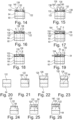
- the silicon core of the guide 25 comprises a horizontal strip 100 and an edge 102 superimposed on this strip 100.
- Such a conformation of the guide 25 is called a “rib waveguide” in English).
- This edge conformation is represented on the figures 5 to 8 .
- the cross section of the strip 100 is rectangular.
- the strip 100 therefore has a horizontal lower face directly in contact with the upper face of the layer 64 and, on the opposite side, a horizontal upper face. It also has 100g and 100d sidewalls ( Figure 5 ). The 100g and 100d sidewalls extend vertically.
- the cross section of the edge 102 is also rectangular. It has a horizontal lower face which is flush with the upper face of the strip 100 and, on the opposite side, a horizontal upper face. It also has 102g and 102d sidewalls ( Figure 5 ) which extend vertically.
- the side walls 100g, 100d, 102g and 102d and the upper face of the edge 102 are encapsulated in a block 104 of silicon nitride.
- This block 104 completely covers the side walls 100g, 100d, 102g, 102d and the upper face of the edge 102 at the locations of the cross sections A to D.
- the sheath of the waveguide 25 is here made of silicon nitride at least along its lateral sides and its upper face.
- the thin thickness of silicon nitride which covers the upper face of the guide 25 is not visible.
- the block 104 is separated from the waveguide 28 by a thin layer 106 of dielectric material.
- the waveguide 28 is separated from the waveguide 25 by the layer 106 and by the silicon nitride which covers the upper face of the guide 25.
- the cross section of the edge 102 gradually widens going from left to right so as to form facing zones in the waveguides 25 and 28 whose effective propagation indices are equal.
- the cross section of the strip 100 remains constant.
- the waveguide 28 ends in an absorption zone 110.
- This zone 110 is located after the coupler 32 and shaped to evacuate the residual fraction of the optical signal which has not been transferred, by the coupler 32, into the waveguide 25.
- the cross section of the edge 102 ( Figure 8 : section D) gradually shrinks until it disappears.
- the lateral sides 102g and 102d gradually approach each other until they reach one end of the edge 102 beyond which this edge 102 no longer exists.
- This narrowing of the cross section of the edge 102 forms a first pointed termination.
- the optical signal is therefore essentially confined within the band 100.
- the cross section of band 100 remains constant.
- the cross section of the waveguide 36 is here rectangular. It therefore has a horizontal lower face directly mechanically supported on the upper face of layer 64 and, on the opposite side, a horizontal upper face. This waveguide 36 is therefore located at the same level as the waveguide 25. In fact, the lower horizontal faces of the waveguides 25 and 36 are located in the same horizontal plane.
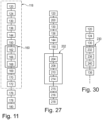
- a method of manufacturing the laser source 10 will now be described using the figures 11 to 26 .
- the substrate 60 is not shown.
- the process begins with a phase 118 of manufacturing the mixed layer 66 on the layer 64.
- This phase 118 begins with a step 120 of providing a stack comprising, immediately stacked on top of each other, the substrate 60, the layer 64 buried oxide and a layer 122 ( Figure 20 ) of monocrystalline silicon.
- a stack is known by the acronym SOI (“Silicon On Insulator”).
- SOI Silicon On Insulator
- the thickness of layer 64 is generally greater than 1 ⁇ m. For example, here, the thickness of layer 64 is equal to 2 ⁇ m or 3 ⁇ m.
- the thickness of layer 122 is smaller and, generally, less than 1 ⁇ m. For example, in this embodiment, the thickness of layer 122 is equal to 500 nm.
- the layer 122 is structured to produce the silicon core of the waveguide 25.
- photolithography, etching and resin mask removal operations are implemented. artwork.
- partial etching operations are implemented to thin the layer 122 of silicon and leave only a thickness of 300 nm or 150 nm of monocrystalline silicon remaining in places. Then, generally, a total etching operation of layer 122 makes it possible to separate the different photonic components made from monocrystalline silicon from this layer 122.
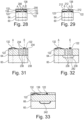
- a sublayer 126 ( Figure 21 ) of silicon oxide is deposited on the top of the waveguide 25.
- a mask 128 ( figures 22 and 23 ), for example made of hard silicon nitride or resin, is deposited above the areas of layer 122 which must not be etched.
- the mask 128 is removed ( Figure 24 ). We then obtain the state represented on the Figure 12 .
- a thin coating 132 ( Figures 13 And 25 ) engraving stop is deposited on the entire upper face.
- the coating 132 is made of silicon nitride.
- the thickness of the coating 132 is typically between 20 nm and 100 nm or between 20 nm and 50 nm.
- This coating 130 covers in particular the upper face of the layer 64 exposed by the total etching carried out during step 124. It also covers the upper face of the core of the waveguide 25.
- Such a coating is known under the English term for “liner”.
- the state obtained after deposition of the coating 132 is represented on the figures 13 And 25 . To simplify the figures 13 to 19 , the residual portions of the oxide sublayer 126 which is located under the coating 132 have not been shown in these figures.
- the coating 132 is deposited by plasma-assisted chemical vapor deposition, that is to say by a process known by the acronym PECVD (“Plasma Enhanced Chemical Vapor Deposition”).
- PECVD Plasma-assisted Chemical Vapor Deposition
- a step 136 of encapsulation of the silicon core and then planarization is carried out.
- a dielectric material 138 ( Figure 14 ) is deposited to encapsulate the silicon core.
- this dielectric material is silicon oxide.
- it is a silicon oxide of the HDP (“high density plasma”) type, or a silicon oxide based on TEOS (“Tetraethylorthosilicate”).
- the deposited thickness of this dielectric material is greater than the maximum thickness of the structured silicon core during the previous stages. Typically this thickness is more than 1.5 times greater than the maximum thickness of the silicon core. In addition, this thickness can be increased depending on the thickness of dielectric material that one wishes to obtain above the silicon core.
- the upper face is planarized by implementing chemical mechanical polishing, better known by the acronym CMP (“Chemical Mechanical Planarization”).
- CMP Chemical Mechanical Planarization
- This planarization operation is stopped when the coating 132 located above the portions of the waveguide 25 whose thickness is equal to 500 nm are exposed.
- the etching agent used during this chemical mechanical polishing operation is a selective etching agent which dissolves at least two or four times more quickly the dielectric material 138 than silicon nitride.
- the upper face is flat.
- a new underlayer 140 ( figures 14 and 26 ) of silicon oxide is deposited in order to obtain an upper face made entirely of silicon oxide.
- the thickness of the sub-layer 140 is chosen so as to adjust the thickness of the silicon nitride core of the waveguide 36 and the thickness of the block 104.
- the thickness of the sub-layer -layer 140 is chosen equal to 40 nm.
- the encapsulated silicon layer represented on the Figure 14 is obtained.
- this trench includes an extension 148 ( Figure 15 ) along the core of the waveguide 25 at the location where the silicon nitride block 104 must be formed.
- this extension 148 exposes the lateral flanks of the core of the waveguide 25.
- the trench 146 and its extension 148 are produced by dry etching, through a mask, of the underlayer 140 and the material 138.
- the dry etching is stopped when the coating 132, located at the location of the trench 146 is exposed.
- the etchant used is a selective etchant which dissolves silicon oxide two or four times more quickly than silicon nitride.
- a layer 152 ( Figure 16 ) of silicon nitride is deposited on the entire exterior face.
- the thickness of layer 152 is sufficient to completely fill trench 146 and its extension 148.
- the thickness of layer 152 is greater than 600 nm.
- layer 152 is deposited by the PECVD process.
- a step 160 the portions of the layer 152 deposited outside the trench 146 and its extension 148 are removed.
- a layer 164 ( Figure 17 ) of silicon oxide is deposited over the entire upper face of layer 152.
- the thickness of layer 164 is sufficient to completely fill the hollows formed in layer 152 directly above trench 146 and its extension 148
- the thickness of layer 164 is greater than 100 nm or 150 nm.
- the layer 164 is planarized by mechanical-chemical polishing.
- polishing is stopped when the upper face of layer 152 is reached.
- operation 166 is carried out like the planarization operation described with reference to step 136.
- an exterior face essentially made up of silicon nitride and a little silicon oxide directly above the trench 146 and the extension 148.
- the black dots directly above trench 146 and its extension 148 represent the silicon oxide residues directly above these elements.
- a non-selective etching operation 168 is executed.
- the etching agent used dissolves silicon oxide as quickly as silicon nitride.
- the etching speed of element B is between 0.8v A and 1.2v A and, preferably, between 0.9v A and 1.1v A , where v A is the etching speed of element A.
- Operation 168 is stopped when the silicon oxide located under layer 152 is reached. For this, the end of this non-selective etching is detected by species detection. Detection by “species detection” is better known under the English expression “optical emission spectroscopy”.
- This process makes it possible to identify the material present on the exterior face being engraved. As soon as the identified material is the dielectric material under layer 152, the non-selective etching is stopped. However, in practice, a small thickness, of the order of 20 nm, of dielectric material located under layer 152 is still consumed. The non-selective etching applied to the planarized face of layer 164 makes it possible to maintain the initial flatness. Thus, at the end of operation 168, a flat exterior face on which the upper faces of the block 104 and the core of the waveguide 36 are flush is obtained. The step 160 of removing the silicon nitride layer 152 is then completed.
- step 160 and during a step 169 localized etching operations of the upper face of the waveguide 36 are carried out. These operations are, for example, implemented to structure the reflector 14 in the waveguide 36.
- the sublayer 106 of dielectric material is deposited on the exterior face.
- the dielectric material deposited during step 170 is silicon oxide.
- step 170 is followed by a step 172 of planarization of the sublayer 106.
- the thickness of the sublayer 106 is equal to 20 nm.
- Phase 118 of manufacturing the mixed layer 66 is then completed.
- the sticker or the substrate is structured by etching to form the core of the waveguide 28.
- the upper sub-layers of the sticker are etched to structure the amplifier 30.
- the sublayer 70 is etched to finalize the structuring of the amplifier 30.
- the resistor 80 is also manufactured.
- the envelope 90 and the sockets 74, 76, 82 and 84 are produced.
- the layer 68 of encapsulated III-V material is then obtained and the manufacturing of the laser source 10 is completed.
- Step 200 is identical to step 124, except that the thickness of the underlayer 126 is greater than 20 nm so as to obtain a greater safety margin when removing the coating 132.
- the thickness of the sublayer 126 is greater than 30 nm or 40 nm.
- the thickness of the sublayer 126 is equal to 40 nm.
- Step 202 begins with an operation 204 of forming a mask 206 ( Figure 28 ) of protection directly above the trench 146 and its extension 148.
- This mask 206 is designed to prevent the etching of the silicon nitride located under this mask.
- mask 206 is made of resin. We then obtain the state represented on the Figure 28 .
- a non-selective etching operation 208 of the silicon nitride is executed. This operation 208 is stopped when the silicon oxide located under layer 152 is exposed. For example, this operation is carried out as described in the context of operation 168.
- the mask 206 is removed.
- the mask 206 is removed.
- This protrusion 212 projects beyond the exterior face of silicon oxide.
- the exterior face is essentially made of silicon oxide, that is to say that the protuberance 212 covers less than 75% and, typically, less than 50% or less than 25% of the exterior face.
- the rest of the exterior face is made of silicon oxide.
- the exterior face is planarized by implementing mechanical-chemical polishing to eliminate the protuberance 212.
- the operation 214 is stopped when the underlayer 126 is reached. .
- Operation 214 still reduces the thickness of the sublayer 126 by 20 nm. Step 202 of removing the layer 152 is then completed.
- the thickness of the deposited sublayer 106 is greater than 50 nm or 80 nm.
- the thickness of the deposited sublayer 106 is equal to 80 nm.
- FIG 30 represents a third method of manufacturing the mixed layer 66 capable of being implemented in place of phase 118 in the process of the Figure 11 .
- This third process is identical to phase 118, except that it includes, between steps 130 and 136, an additional step 230 of creating a cavity under the waveguide 36.
- openings 234 extend along the location where the guide 36 must be made.
- these openings 234 also extend along the location where the block 104 must be made.
- trenches 238 crossing right through the thickness of the layer 64 are produced using the coating 132 as an etching mask. These trenches 238 each open onto the substrate 60. We then obtain the state shown on the Figure 31 .
- an etching of the substrate 60 is carried out to form a cavity 242 inside the substrate 60.
- a selective etching agent is introduced into the trenches 238.
- This etching agent dissolves two or four times faster silicon than silicon oxide.
- this is an anisotropic etching agent, that is to say an etching agent which dissolves silicon at the same speed in both the vertical direction and the horizontal direction.
- the cavity 242 extends under the location where the guide 36 and the block 104 must be made.
- the cavity 242 also extends under the location where the guide 36 and the block 104 must be made. made the coupler 34.
- trenches 238 are filled in. For example, here, this is carried out during step 136. In fact, the deposition of the dielectric material 138 during step 136 closes the trenches 238. We then obtain, at the end of step 136, the state shown on the Figure 33 .
- step 136 the method of manufacturing the mixed layer 66 is for example identical to what has already been described with reference to the figure 11 or 27 .
- the dotted lines on the figure 30 indicate that the steps following step 136 have not been represented.
- the cavity 242 makes it possible to move the guide 36 away from the substrate 60 and to better insulate this guide 36 from the substrate 60. This improvement in the insulation between the waveguide 36 and the substrate 60 reduces optical losses, particularly when the dimensions transverse of the guide 36 are small.
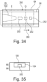
- THE figures 34 and 35 represent a coupler 250 with an inverted tip capable of being used in place of the coupler 34.
- the dotted line G on the Figure 34 represents the location of the cross section G of the coupler 250.
- the Figure 35 represents the cross section G.
- the coupler 250 is identical to the coupler 34, except that the tip termination of the band 100 of the waveguide 25 is replaced by a tip termination with sub-wavelength patterns.
- the coupler 250 comprises patterns 252 aligned one behind the other in the direction 260 of propagation of the optical signal at the wavelength ⁇ Li .
- Each pattern 252 is made of silicon and entirely encapsulated in the block 104 of silicon nitride. The horizontal dimensions of these patterns are less than the wavelength ⁇ Li .
- the length of the patterns 252 in the direction 260 decreases as one moves away from the pointed termination.
- the cross section of each pattern 252 is for example rectangular.
- the coupler 250 comprises three patterns 252.
- the waveguide 15 can be made of silicon.
- waveguide 25 is possible.
- edge 102 is omitted.
- conformation of the waveguide 25 is called “slab waveguide” in English.
- the coupler 34 has a single pointed termination, that is to say that produced by narrowing the cross section of the strip 100.
- the upper face of the edge 102 is flush with the upper face of the block 104.
- the sheath of the waveguide 25 is not necessarily made of silicon nitride. It can also be made of silicon oxide for example. In this case, the silicon nitride block 104 is omitted in the portion of the guide 25 located before the coupler 34. The dielectric material located between the waveguides 28 and 25 then has no thickness of silicon nitride.
- couplers 26 and 32 can be made differently.
- the point termination can be made in the guide 25 and/or in the guide 28.
- couplers 24 and 34 are possible.
- these couplers are not necessarily made using a reverse tip transition.
- the cross section of the waveguide 25 is small, that is to say typically less than 100 nm x 100 nm, then an optical coupling known under the English term "Butt coupling" can be implemented.
- the sheath of the waveguide 25 is generally made entirely of a dielectric material other than silicon nitride, such as silicon oxide.
- the filter 22 is made in the silicon waveguide 25.
- the laser source has been described in the particular case where it is a DBR (“Distributed Bragg Reflector”) laser source.
- a mixed layer such as the mixed layer 66 can also be used to produce a DFB (“Distributed FeedBack”) laser source.
- the silicon nitride waveguide is also located in the extension of the silicon waveguide produced under the waveguide in III-V material.
- the Bragg grating is produced in the silicon waveguide or in a silicon nitride sublayer interposed between the silicon waveguide and the waveguide in III-V material.
- layer 122 can also be made of amorphous silicon.
- step 124 of structuring the silicon core are possible.
- silicon oxide sublayer 126 may be omitted.
- the structuring of the silicon core can also include localized growth operations or by growth of monocrystalline silicon or by deposition of amorphous silicon, or by deposition of amorphous silicon followed by recrystallization by heat treatment to locally increase the thickness of the silicon core.
- the initial thickness of the monocrystalline silicon layer 122 can be reduced.
- the initial thickness of layer 122 is then 300 nm.
- the etching stop coating 132 can be made from materials other than silicon nitride.
- it can be made from Al 2 O 3 or HfO 2 .
- the lower face of the guide 36 is located at a level slightly above the lower face of the guide 25. Typically, the difference in height between these two lower faces, however, remains less than 100 nm and, generally, less than 50nm.
- a material other than silicon oxide can be used as long as the material can be planarized then etched as described during operations 166 and 168.
- the mechanical-chemical polishing of the silicon oxide layer can also be stopped before reaching the silicon nitride layer 152.
- a residual layer of silicon oxide which completely covers the nitride layer 152. of silicon. Then, this residual layer is completely eliminated during the non-selective etching operation 168.
- the non-selective etching operation 168 is continued until the coating 132 or the sub-layer 126 is reached. In this case, at least part or all of the silicon nitride coating 132 is also eliminated. .
- a dielectric material other than silicon oxide can be deposited to form the underlayer 106.
- this other material is then chosen to allow good direct bonding of the sticker or the substrate in material III-V.
- step 176 instead of sticking a sticker or a substrate made of III-V gain material, it is possible to deposit this material on the mixed layer 66.
- the operation 208 of non-selective etching of the silicon nitride is stopped before reaching the sub-layer 126. For example, it is stopped when the sub-layer 140 is reached.
- the phase of manufacturing a mixed layer can be implemented in processes other than a process for manufacturing a laser source.
- the method described is also suitable for the manufacture of a mixed layer in which the silicon and silicon nitride waveguides contained in this mixed layer are not optically coupled to each other by a optical coupler such as couplers 24 and 34.
- the optical coupling between these two waveguides can be carried out using an optical coupler of which at least part is produced in a layer located above or below the mixed layer.
- the methods described here also make it possible to produce a mixed layer in which the silicon and silicon nitride waveguides are not optically coupled to each other. In this case, the production of an optical coupler such as couplers 24 and 34 is omitted.
- the methods described here for manufacturing a mixed layer can also be implemented in processes for manufacturing photonic components which do not include a layer of encapsulated III-V material.
- the mixed layer may include additional waveguides made of silicon or silicon nitride.
- additional waveguides made of silicon or silicon nitride.
- one of these additional waveguides is optically connected at the output of reflector 12 or 14.
- the incoming optical signal is absorbed instead of being amplified.
- the amplifier 30 is then used to carry out photo-detection or modulation of signals.
- these photonic components and in particular the photonic components comprising a layer of III-V material stacked on the mixed layer such as the laser source 10, can be manufactured using another method of manufacturing the mixed layer 66 than those described here.
- the embodiments of the laser source described here can be implemented independently of the methods which have been described for manufacturing this mixed layer.
- the methods for manufacturing a mixed layer described here are simple. In fact, they do not require any turning of the substrate. From then on, all the etching, planarization and deposition steps to produce the mixed layer are carried out from the same side of this substrate 60.
- the methods for manufacturing a mixed layer described here also make it possible to obtain a greater integration density than known methods.
- known methods implement the transfer of a silicon nitride sticker and/or a monocrystalline silicon sticker onto layer 64.
- a space of several hundred micrometers must necessarily exist between these silicon and silicon nitride stickers. Therefore, the silicon and silicon nitride cores produced by structuring these vignettes are necessarily spaced from each other by several hundred micrometers.
- barrier coating makes it possible to precisely position the bottom of the trench 146 less than 100 nm from the upper face of the layer 64.
- the coating 132 is made of silicon nitride
- the lower faces of the silicon and silicon nitride cores are located in the same horizontal plane.
- Forming the sheath of the guide 25 in silicon nitride makes it possible to improve the optical properties of the silicon waveguide.
- a mixed layer to manufacture a photonic component makes it possible to increase the integration density of this photonic component. Indeed, it is no longer necessary to have the silicon waveguides in a first layer and the silicon nitride waveguides in a second layer located above or below this first layer.
Landscapes
- Physics & Mathematics (AREA)
- General Physics & Mathematics (AREA)
- Optics & Photonics (AREA)
- Condensed Matter Physics & Semiconductors (AREA)
- Electromagnetism (AREA)
- Engineering & Computer Science (AREA)
- Microelectronics & Electronic Packaging (AREA)
- Optical Integrated Circuits (AREA)
Claims (11)
- Verfahren zur Herstellung einer gemischten Schicht, die einen ersten Wellenleiter, dessen Kern aus Silicium ist, und einen zweiten Wellenleiter, dessen Kern aus Siliciumnitrid ist, enthält, wobei das Verfahren die folgenden Schritte umfasst:1) das Bereitstellen (120) eines Substrats, auf dem in der Reihenfolge eine Schicht aus vergrabenem dielektrischem Material und eine Schicht aus Silicium gestapelt sind, wobei sich dieses Substrat im Wesentlichen in einer Ebene, "Ebene des Substrats" genannt, erstreckt und sich die verschiedenen Schichten parallel zu der Ebene des Substrats erstrecken, dann2) das Strukturieren (124) der Schicht aus Silicium, um den Kern aus Silicium des ersten Wellenleiters zu bilden, dann3) das Kapseln (136) des gebildeten Kerns aus Silicium in dielektrisches Material, dann das Planarisieren des dielektrischen Materials, wobei dieses Kapseln und das anschließende Planarisieren eine Schicht aus gekapseltem Silicium bilden, die den Kern aus Silicium enthält,dadurch gekennzeichnet, dass das Verfahren anschließend die folgenden Schritte umfasst:4) das Ausführen (144) eines Grabens in der Schicht aus gekapseltem Silicium an der Stelle, an welcher der Kern aus Siliciumnitrid des zweiten Wellenleiters ausgeführt werden soll, dann5) das Abscheiden (150) einer Siliciumnitridschicht auf der Schicht aus gekapseltem Silicium, wobei diese Siliciumnitridschicht die Schicht aus gekapseltem Silicium vollständig bedeckt und wobei die Dicke der abgeschiedenen Siliciumnitridschicht ausreichend ist, um den Graben vollständig zu füllen, dann6) das Abtragen (160; 202) des außerhalb des Grabens gelegenen Siliciumnitrids, um eine Oberseite der gekapselten Schicht aus Silicium freizulegen, mit welcher der mit Siliciumnitrid gefüllte Graben bündig ist, und so den Kern aus Siliciumnitrid des zweiten Wellenleiters zu erhalten, dann7) das Abscheiden (170; 216) einer Schicht aus dielektrischem Material, welche die freigelegte Oberseite bedeckt, um das Kapseln des Kerns aus Siliciumnitrid abzuschließen und so die gemischte Schicht zu erhalten, die gleichzeitig die Kerne aus Silicium und aus Siliciumnitrid enthält, die in dielektrisches Material gekapselt sind.
- Verfahren nach Anspruch 1, wobei das Abtragen des Siliciumnitrids umfasst:- das Abscheiden (162) einer Schicht aus Siliciumoxid auf der gesamten abgeschiedenen Siliciumnitridschicht, dann- das chemisch-mechanische Polieren (166) dieser Siliciumoxidschicht, um eine Außenseite zu erhalten, die ebener als die Außenseite der abgeschiedenen Siliciumnitridschicht ist, dann- das nicht selektive Ätzen (168) der Außenseite, bis ein dielektrisches Material freigelegt wird, das unter der Siliciumnitridschicht gelegen ist, und so eine ebene Oberseite erhalten wird, mit welcher der mit Siliciumnitrid gefüllte Graben bündig ist, wobei dieses nicht selektive Ätzen ausgeführt wird, indem diese Außenseite einem Ätzmittel ausgesetzt wird, welches das Siliciumoxid ebenso schnell löst wie das Siliciumnitrid.
- Verfahren nach Anspruch 1, wobei das Abtragen des Siliciumnitrids umfasst:- das Bilden (204) einer Schutzmaske, die einen Bereich der Schicht aus Siliciumnitrid bedeckt, der in der Lotrechten über dem Graben gelegen ist, und den überwiegenden Teil der Außenseite der Schicht aus Siliciumnitrid frei lässt, die direkt der Außenumgebung ausgesetzt ist, dann- das Ätzen (208) der Außenseite der Schicht aus Siliciumnitrid, bis ein dielektrisches Material freigelegt wird, das unter dieser Siliciumnitridschicht gelegen ist, wobei bei diesem Ätzen das verwendete Ätzmittel das Siliciumnitrid zehn Mal schneller löst als die Schutzmaske, dann- das Abtragen (210) der Schutzmaske, um eine Außenseite zu erhalten, die aus dem freigelegten dielektrischen Material und aus Höckern aus Siliciumnitrid an der Stelle der abgetragenen Schutzmaske gebildet wird, dann- das chemisch-mechanische Polieren (214) der Außenseite, welche die Höcker aus Siliciumnitrid umfasst, um die Oberseite der Schicht aus gekapseltem Silicium zu erhalten, mit welcher der mit Siliciumnitrid gefüllte Graben bündig ist.
- Verfahren nach einem der vorhergehenden Ansprüche, wobei das Verfahren nach dem Schritt 2) und vor dem Schritt 3) umfasst:- das Abscheiden (130), auf der Schicht aus vergrabenem dielektrischem Material und an der Stelle, an welcher der Graben ausgeführt werden soll, einer Ätzstopp-Beschichtung, deren Dicke weniger als 100 nm beträgt, dann- beim Schritt 3) das zum Kapseln des Kerns aus Silicium verwendete dielektrische Material verschieden von dem zum Bilden der Ätzstopp-Beschichtung verwendeten Material ist und- der Schritt 4) umfasst:- das Ausführen des Grabens durch Ätzen durch eine Maske hindurch, die nur die Oberseite der Schicht aus gekapseltem Silicium an der Stelle aussetzt, an der dieser Graben ausgeführt werden soll, wobei das verwendete Ätzmittel das zum Kapseln des Kerns aus Silicium verwendete dielektrische Material mindestens zwei Mal schneller löst als das zum Ausführen der Ätzstopp-Beschichtung verwendete Material, dann- das Stoppen dieses Ätzens, wenn die Stopp-Beschichtung erreicht ist.
- Verfahren nach Anspruch 4, wobei die Ätzstopp-Beschichtung aus Siliciumnitrid ausgeführt ist.
- Verfahren nach einem der vorhergehenden Ansprüche, wobei:- der Schritt 2) das Strukturieren (124) des Kerns aus monokristallinem Silicium mit seitlichen Flanken umfasst, die sich an einem Ende dieses Kerns aus monokristallinem Silicium einander annähern, um eine Zuspitzung zu bilden, jenseits der das optische Signal sich nicht mehr im Inneren des Wellenleiters aus Silicium ausbreitet,- der Schritt 4) das Ausführen (144) einer Verlängerung des Grabens umfasst, wobei diese Verlängerung die seitlichen Flanken des Kerns aus Silicium mindestens an seiner Zuspitzung freilegt, und- beim Schritt 5) das Abscheiden (150) der Siliciumnitridschicht auch einen Block aus Siliciumnitrid bildet, der die freigelegten seitlichen Flanken des Kerns aus Silicium bedeckt.
- Verfahren nach Anspruch 6, wobei:- beim Schritt 4) das Ausführen (144) der Verlängerung des Grabens die seitlichen Flanken des Kerns aus Silicium über die gesamte Länge des Kerns aus Silicium freilegt und- beim Schritt 5) das Abscheiden (150) der Siliciumnitridschicht einen Block aus Siliciumnitrid bildet, der die Gesamtheit der seitlichen Flanken des Kerns aus Silicium vollständig bedeckt, wobei dieser Block aus Siliciumnitrid somit einen Abschnitt des Mantels des Wellenleiters aus Silicium bildet.
- Verfahren zur Herstellung eines photonischen III-V-Halbleiter-Bauelements, wobei dieses Verfahren umfasst:- das Herstellen (118) einer gemischten Schicht gemäß einem der vorhergehenden Ansprüche, die einen ersten Wellenleiter, dessen Kern aus Silicium ist, und einen zweiten Wellenleiter, dessen Kern aus Siliciumnitrid ist, enthält, dann- das Ausführen (176) einer Dicke aus III-V-Material direkt auf der hergestellten gemischten Schicht, dann- das Strukturieren (178) der Dicke aus III-V-Material, um den Kern eines dritten Wellenleiters aus III-V-Material zu bilden, dann- das Kapseln (180) des Kerns des dritten Wellenleiters in ein dielektrisches Material, um den Mantel dieses dritten Wellenleiters zu bilden, und- das Ausführen (124, 178) einer adiabatischen Kopplung zwischen dem dritten Wellenleiter und dem ersten Wellenleiter.
- Photonisches III-V-Halbleiter-Bauelement, das nach dem Verfahren des Anspruchs 8 hergestellt wird, dadurch gekennzeichnet, dass dieses photonische Bauelement umfasst:- ein Substrat (60), auf dem in der Reihenfolge gestapelt sind:- eine gemischte Schicht (66), die einen ersten Wellenleiter (25), dessen Kern aus Silicium ist, und einen zweiten Wellenleiter (36), dessen Kern aus Siliciumnitrid ist, enthält, und- eine Schicht (68) aus gekapseltem III-V-Material, die den Kern eines dritten Wellenleiters (28) aus III-V-Material enthält, wobei sich dieses Substrat im Wesentlichen in einer Ebene, "Ebene des Substrats" genannt, erstreckt und sich die verschiedenen Schichten parallel zu der Ebene des Substrats erstrecken, und- eine adiabatische Kopplung (26, 32) zwischen dem dritten Wellenleiter und dem ersten Wellenleiter.
- Photonisches Bauelement nach Anspruch 9, wobei:- der Kern des ersten Wellenleiters erste und zweite seitliche Flanken (100g, 100d, 102g, 102d) umfasst, die sich jeweils in einer senkrecht zur Ebene des Substrats verlaufenden Richtung erstrecken, und die seitlichen Flanke sich an einem Ende des ersten Wellenleiters einander nähern, um eine Zuspitzung zu bilden, jenseits der sich das optische Signal nicht mehr im Inneren des ersten Wellenleiters, sondern im Inneren des zweiten Wellenleiters ausbreiten,- der Abschnitt des Mantels des ersten Wellenleiters (25), der die seitlichen Flanken des Kerns aus Silicium über die gesamte Länge der Zuspitzung bedeckt, aus Siliciumnitrid ausgeführt ist,- der Kern aus Siliciumnitrid des zweiten Wellenleiters (36) im Inneren der gemischten Schicht in der Verlängerung der Zuspitzung des Kerns aus Silicium gelegen ist und- der Kern aus Siliciumnitrid des zweiten Wellenleiters (36) einen einzigen Materialblock mit dem Abschnitt des Mantels des ersten Wellenleiters bildet, der die seitlichen Flanken der Zuspitzung des Kerns aus Silicium bedeckt, um diesen zweiten Wellenleiter optisch mit dem ersten Wellenleiter zu koppeln.
- Photonisches Bauelement nach Anspruch 10, wobei das photonische Bauelement eine Laserquelle ist, die geeignet ist, ein optisches Signal mit mindestens einer Wellenlänge λLi auszusenden, wobei diese Laserquelle einen optischen Hohlraum umfasst, der geeignet ist, das optische Signal mit der Wellenlänge λLi resonieren zu lassen, wobei dieser optische Hohlraum umfasst:- den dritten Wellenleiter (28), wobei der Kern dieses dritten Wellenleiters aus III-V-Verstärkungsmaterial ausgeführt ist, um das optische Signal mit der Wellenlänge λLi zu verstärken, das sich entlang des Kerns dieses dritten Wellenleiters ausbreitet, wobei dieser dritte Wellenleiter im Inneren der Schicht aus gekapseltem III-V-Material gelegen ist,- den ersten Wellenleiter (25), dessen Kern aus Silicium ausgeführt ist,- den zweiten Wellenleiter (36), dessen Kern aus Siliciumnitrid ausgeführt ist.
Applications Claiming Priority (2)
| Application Number | Priority Date | Filing Date | Title |
|---|---|---|---|
| FR2003653A FR3109242B1 (fr) | 2020-04-10 | 2020-04-10 | Procédé de fabrication d’une couche mixte comportant un guide d’onde en silicium et un guide d’onde en nitrure de silicium |
| PCT/EP2021/058847 WO2021204749A1 (fr) | 2020-04-10 | 2021-04-06 | Procédé de fabrication d'une couche mixte comportant un guide d'onde en silicium et un guide d'onde en nitrure de silicium |
Publications (2)
| Publication Number | Publication Date |
|---|---|
| EP4133317A1 EP4133317A1 (de) | 2023-02-15 |
| EP4133317B1 true EP4133317B1 (de) | 2024-06-05 |
Family
ID=72178660
Family Applications (1)
| Application Number | Title | Priority Date | Filing Date |
|---|---|---|---|
| EP21716431.8A Active EP4133317B1 (de) | 2020-04-10 | 2021-04-06 | Verfahren zur herstellung einer mischschicht mit einem siliziumwellenleiter und einem siliziumnitridwellenleiter |
Country Status (5)
| Country | Link |
|---|---|
| US (1) | US12174425B2 (de) |
| EP (1) | EP4133317B1 (de) |
| FR (1) | FR3109242B1 (de) |
| TW (1) | TWI865766B (de) |
| WO (1) | WO2021204749A1 (de) |
Families Citing this family (6)
| Publication number | Priority date | Publication date | Assignee | Title |
|---|---|---|---|---|
| GB2607361B (en) * | 2021-06-01 | 2024-12-18 | Rockley Photonics Ltd | Laser with wavelength-selective reflector |
| CN116413853A (zh) * | 2021-12-31 | 2023-07-11 | 上海新微技术研发中心有限公司 | 一种多层波导结构 |
| CN114400236B (zh) * | 2022-01-16 | 2024-04-26 | Nano科技(北京)有限公司 | 集成硅光调制器和锗硅探测器的硅光集成芯片及制备方法 |
| TWI868903B (zh) * | 2023-09-06 | 2025-01-01 | 世界先進積體電路股份有限公司 | 矽光子平臺、複合平臺的製作方法、及矽光子平臺的製作方法 |
| US12541054B2 (en) * | 2023-09-29 | 2026-02-03 | Taiwan Semiconductor Manufacturing Company, Ltd. | Photonic device and method of fabricating same |
| US20250208445A1 (en) * | 2023-12-20 | 2025-06-26 | Taiwan Semiconductor Manufacturing Company, Ltd. | Semiconductor photonics device and methods of formation |
Family Cites Families (13)
| Publication number | Priority date | Publication date | Assignee | Title |
|---|---|---|---|---|
| US7199398B2 (en) * | 2002-11-20 | 2007-04-03 | Sharp Kabushiki Kaisha | Nitride semiconductor light emitting device having electrode electrically separated into at least two regions |
| US9711534B2 (en) * | 2011-10-28 | 2017-07-18 | Hewlett Packard Enterprise Development Lp | Devices including a diamond layer |
| WO2013119981A1 (en) * | 2012-02-10 | 2013-08-15 | Massachusetts Institute Of Technology | Athermal photonic waveguide with refractive index tuning |
| US9136672B2 (en) * | 2012-11-29 | 2015-09-15 | Agency For Science, Technology And Research | Optical light source |
| FR3007589B1 (fr) * | 2013-06-24 | 2015-07-24 | St Microelectronics Crolles 2 | Circuit integre photonique et procede de fabrication |
| US9450379B2 (en) * | 2013-11-20 | 2016-09-20 | Coriant Advanced Technology, LLC | Quantum dot SOA-silicon external cavity multi-wavelength laser |
| US9864138B2 (en) * | 2015-01-05 | 2018-01-09 | The Research Foundation For The State University Of New York | Integrated photonics including germanium |
| FR3046705B1 (fr) | 2016-01-08 | 2018-02-16 | Commissariat Energie Atomique | Source laser a semi-conducteur |
| US9671557B1 (en) * | 2016-03-04 | 2017-06-06 | Inphi Corporation | Vertical integration of hybrid waveguide with controlled interlayer thickness |
| FR3068527A1 (fr) | 2017-06-29 | 2019-01-04 | Commissariat A L'energie Atomique Et Aux Energies Alternatives | Source laser a semi-conducteur |
| WO2019027631A1 (en) | 2017-07-31 | 2019-02-07 | Dow Global Technologies Llc | DETERGENT ADDITIVE |
| CN110954998B (zh) * | 2018-09-27 | 2021-10-01 | 上海新微技术研发中心有限公司 | 激光器与硅光芯片集成结构及其制备方法 |
| US11187532B2 (en) * | 2020-03-06 | 2021-11-30 | Anello Photonics, Inc. | Process flow for fabricating integrated photonics optical gyroscopes |
-
2020
- 2020-04-10 FR FR2003653A patent/FR3109242B1/fr active Active
-
2021
- 2021-04-06 EP EP21716431.8A patent/EP4133317B1/de active Active
- 2021-04-06 US US17/995,875 patent/US12174425B2/en active Active
- 2021-04-06 WO PCT/EP2021/058847 patent/WO2021204749A1/fr not_active Ceased
- 2021-04-09 TW TW110112908A patent/TWI865766B/zh active
Also Published As
| Publication number | Publication date |
|---|---|
| US12174425B2 (en) | 2024-12-24 |
| TW202230468A (zh) | 2022-08-01 |
| FR3109242B1 (fr) | 2022-03-18 |
| WO2021204749A1 (fr) | 2021-10-14 |
| FR3109242A1 (fr) | 2021-10-15 |
| US20230168429A1 (en) | 2023-06-01 |
| TWI865766B (zh) | 2024-12-11 |
| EP4133317A1 (de) | 2023-02-15 |
Similar Documents
| Publication | Publication Date | Title |
|---|---|---|
| EP4133317B1 (de) | Verfahren zur herstellung einer mischschicht mit einem siliziumwellenleiter und einem siliziumnitridwellenleiter | |
| EP3206079B1 (de) | Photonischer sender | |
| EP3540878B1 (de) | Photonenvorrichtung, die einen laser umfasst, der optisch mit einem silizium-wellenleiter verbunden ist, und herstellungsverfahren einer solchen photonenvorrichtung | |
| EP3190672B1 (de) | Laserquelle mit halbleiter | |
| EP3168946B1 (de) | Laservorrichtung und herstellungsverfahren einer solchen laservorrichtung | |
| EP2411863B1 (de) | Aus Silizium auf einem Isolator bestehender optischer Breitbandmodulator | |
| EP3497512B1 (de) | Verfahren zur herstellung eines modulators der ausbreitung und von ausbreitungsindexverlusten eines optischen signals | |
| EP3599684B1 (de) | Photonischer sender | |
| EP3339924A1 (de) | Optimierter integrierter photonenschaltkreis | |
| EP2843451A1 (de) | Herstellungsverfahren eines streifenförmigen PIN-Übergangs mit getrennten dotierten Schichten, und Anwendung bei der Herstellung von elektro-optischen Modulatoren und Fotodetektoren | |
| EP4163684B1 (de) | Photonenchip | |
| EP2988378A1 (de) | Laservorrichtung und herstellungsverfahren einer solchen laservorrichtung | |
| WO2019002763A1 (fr) | Source laser à semi-conducteur | |
| EP4198587A1 (de) | Verfahren zur herstellung eines photonischen chips | |
| EP3822698B1 (de) | Photonischer sender | |
| EP3654463A1 (de) | Laserquelle mit halbleiter | |
| EP3276385B1 (de) | Herstellungsverfahren eines langsamen wellenleiters aus germanium, und fotodiode, in die ein solcher langsamer wellenleiter eingebaut ist | |
| EP3654462B1 (de) | Laserquelle mit halbleiter und emissionsverfahren mit dieser laserquelle | |
| EP3389097B1 (de) | Fotodiode | |
| EP3772145A1 (de) | Hybride laserquelle, die einen integrierten wellenleiter mit einem zwischengeschalteten bragg-gitter umfasst | |
| EP4148470A1 (de) | Verfahren zur herstellung eines optoelektronischen systems mit silizium-photonik, das eine optische vorrichtung umfasst, die mit einer integrierten photonischen schaltung gekoppelt ist | |
| EP4286926B1 (de) | Verfahren zur herstellung eines photonischen chips | |
| FR2854469A1 (fr) | Procede de fabrication d'un dispositif optique semi-conducteur comportant une region munie d'une couche active a epaisseur variable |
Legal Events
| Date | Code | Title | Description |
|---|---|---|---|
| STAA | Information on the status of an ep patent application or granted ep patent |
Free format text: STATUS: UNKNOWN |
|
| STAA | Information on the status of an ep patent application or granted ep patent |
Free format text: STATUS: THE INTERNATIONAL PUBLICATION HAS BEEN MADE |
|
| PUAI | Public reference made under article 153(3) epc to a published international application that has entered the european phase |
Free format text: ORIGINAL CODE: 0009012 |
|
| STAA | Information on the status of an ep patent application or granted ep patent |
Free format text: STATUS: REQUEST FOR EXAMINATION WAS MADE |
|
| 17P | Request for examination filed |
Effective date: 20221006 |
|
| AK | Designated contracting states |
Kind code of ref document: A1 Designated state(s): AL AT BE BG CH CY CZ DE DK EE ES FI FR GB GR HR HU IE IS IT LI LT LU LV MC MK MT NL NO PL PT RO RS SE SI SK SM TR |
|
| DAV | Request for validation of the european patent (deleted) | ||
| DAX | Request for extension of the european patent (deleted) | ||
| GRAP | Despatch of communication of intention to grant a patent |
Free format text: ORIGINAL CODE: EPIDOSNIGR1 |
|
| STAA | Information on the status of an ep patent application or granted ep patent |
Free format text: STATUS: GRANT OF PATENT IS INTENDED |
|
| INTG | Intention to grant announced |
Effective date: 20231122 |
|
| RAP3 | Party data changed (applicant data changed or rights of an application transferred) |
Owner name: THALES Owner name: COMMISSARIAT A L'ENERGIE ATOMIQUE ET AUX ENERGIES ALTERNATIVES |
|
| GRAS | Grant fee paid |
Free format text: ORIGINAL CODE: EPIDOSNIGR3 |
|
| GRAA | (expected) grant |
Free format text: ORIGINAL CODE: 0009210 |
|
| STAA | Information on the status of an ep patent application or granted ep patent |
Free format text: STATUS: THE PATENT HAS BEEN GRANTED |
|
| AK | Designated contracting states |
Kind code of ref document: B1 Designated state(s): AL AT BE BG CH CY CZ DE DK EE ES FI FR GB GR HR HU IE IS IT LI LT LU LV MC MK MT NL NO PL PT RO RS SE SI SK SM TR |
|
| REG | Reference to a national code |
Ref country code: CH Ref legal event code: EP |
|
| REG | Reference to a national code |
Ref country code: DE Ref legal event code: R096 Ref document number: 602021014081 Country of ref document: DE |
|
| REG | Reference to a national code |
Ref country code: IE Ref legal event code: FG4D Free format text: LANGUAGE OF EP DOCUMENT: FRENCH |
|
| REG | Reference to a national code |
Ref country code: LT Ref legal event code: MG9D |
|
| PG25 | Lapsed in a contracting state [announced via postgrant information from national office to epo] |
Ref country code: BG Free format text: LAPSE BECAUSE OF FAILURE TO SUBMIT A TRANSLATION OF THE DESCRIPTION OR TO PAY THE FEE WITHIN THE PRESCRIBED TIME-LIMIT Effective date: 20240605 |
|
| REG | Reference to a national code |
Ref country code: NL Ref legal event code: MP Effective date: 20240605 |
|
| PG25 | Lapsed in a contracting state [announced via postgrant information from national office to epo] |
Ref country code: FI Free format text: LAPSE BECAUSE OF FAILURE TO SUBMIT A TRANSLATION OF THE DESCRIPTION OR TO PAY THE FEE WITHIN THE PRESCRIBED TIME-LIMIT Effective date: 20240605 Ref country code: HR Free format text: LAPSE BECAUSE OF FAILURE TO SUBMIT A TRANSLATION OF THE DESCRIPTION OR TO PAY THE FEE WITHIN THE PRESCRIBED TIME-LIMIT Effective date: 20240605 |
|
| PG25 | Lapsed in a contracting state [announced via postgrant information from national office to epo] |
Ref country code: GR Free format text: LAPSE BECAUSE OF FAILURE TO SUBMIT A TRANSLATION OF THE DESCRIPTION OR TO PAY THE FEE WITHIN THE PRESCRIBED TIME-LIMIT Effective date: 20240906 |
|
| PG25 | Lapsed in a contracting state [announced via postgrant information from national office to epo] |
Ref country code: ES Free format text: LAPSE BECAUSE OF FAILURE TO SUBMIT A TRANSLATION OF THE DESCRIPTION OR TO PAY THE FEE WITHIN THE PRESCRIBED TIME-LIMIT Effective date: 20240605 |
|
| PG25 | Lapsed in a contracting state [announced via postgrant information from national office to epo] |
Ref country code: LV Free format text: LAPSE BECAUSE OF FAILURE TO SUBMIT A TRANSLATION OF THE DESCRIPTION OR TO PAY THE FEE WITHIN THE PRESCRIBED TIME-LIMIT Effective date: 20240605 |
|
| RAP4 | Party data changed (patent owner data changed or rights of a patent transferred) |
Owner name: THALES Owner name: COMMISSARIAT A L'ENERGIE ATOMIQUE ET AUX ENERGIESALTERNATIVES |
|
| PG25 | Lapsed in a contracting state [announced via postgrant information from national office to epo] |
Ref country code: NO Free format text: LAPSE BECAUSE OF FAILURE TO SUBMIT A TRANSLATION OF THE DESCRIPTION OR TO PAY THE FEE WITHIN THE PRESCRIBED TIME-LIMIT Effective date: 20240905 Ref country code: LV Free format text: LAPSE BECAUSE OF FAILURE TO SUBMIT A TRANSLATION OF THE DESCRIPTION OR TO PAY THE FEE WITHIN THE PRESCRIBED TIME-LIMIT Effective date: 20240605 Ref country code: HR Free format text: LAPSE BECAUSE OF FAILURE TO SUBMIT A TRANSLATION OF THE DESCRIPTION OR TO PAY THE FEE WITHIN THE PRESCRIBED TIME-LIMIT Effective date: 20240605 Ref country code: GR Free format text: LAPSE BECAUSE OF FAILURE TO SUBMIT A TRANSLATION OF THE DESCRIPTION OR TO PAY THE FEE WITHIN THE PRESCRIBED TIME-LIMIT Effective date: 20240906 Ref country code: FI Free format text: LAPSE BECAUSE OF FAILURE TO SUBMIT A TRANSLATION OF THE DESCRIPTION OR TO PAY THE FEE WITHIN THE PRESCRIBED TIME-LIMIT Effective date: 20240605 Ref country code: ES Free format text: LAPSE BECAUSE OF FAILURE TO SUBMIT A TRANSLATION OF THE DESCRIPTION OR TO PAY THE FEE WITHIN THE PRESCRIBED TIME-LIMIT Effective date: 20240605 Ref country code: BG Free format text: LAPSE BECAUSE OF FAILURE TO SUBMIT A TRANSLATION OF THE DESCRIPTION OR TO PAY THE FEE WITHIN THE PRESCRIBED TIME-LIMIT Effective date: 20240605 Ref country code: RS Free format text: LAPSE BECAUSE OF FAILURE TO SUBMIT A TRANSLATION OF THE DESCRIPTION OR TO PAY THE FEE WITHIN THE PRESCRIBED TIME-LIMIT Effective date: 20240905 |
|
| PG25 | Lapsed in a contracting state [announced via postgrant information from national office to epo] |
Ref country code: NL Free format text: LAPSE BECAUSE OF FAILURE TO SUBMIT A TRANSLATION OF THE DESCRIPTION OR TO PAY THE FEE WITHIN THE PRESCRIBED TIME-LIMIT Effective date: 20240605 |
|
| REG | Reference to a national code |
Ref country code: AT Ref legal event code: MK05 Ref document number: 1692864 Country of ref document: AT Kind code of ref document: T Effective date: 20240605 |
|
| PG25 | Lapsed in a contracting state [announced via postgrant information from national office to epo] |
Ref country code: NL Free format text: LAPSE BECAUSE OF FAILURE TO SUBMIT A TRANSLATION OF THE DESCRIPTION OR TO PAY THE FEE WITHIN THE PRESCRIBED TIME-LIMIT Effective date: 20240605 |
|
| PG25 | Lapsed in a contracting state [announced via postgrant information from national office to epo] |
Ref country code: PT Free format text: LAPSE BECAUSE OF FAILURE TO SUBMIT A TRANSLATION OF THE DESCRIPTION OR TO PAY THE FEE WITHIN THE PRESCRIBED TIME-LIMIT Effective date: 20241007 |
|
| PG25 | Lapsed in a contracting state [announced via postgrant information from national office to epo] |
Ref country code: PT Free format text: LAPSE BECAUSE OF FAILURE TO SUBMIT A TRANSLATION OF THE DESCRIPTION OR TO PAY THE FEE WITHIN THE PRESCRIBED TIME-LIMIT Effective date: 20241007 |
|
| PG25 | Lapsed in a contracting state [announced via postgrant information from national office to epo] |
Ref country code: PL Free format text: LAPSE BECAUSE OF FAILURE TO SUBMIT A TRANSLATION OF THE DESCRIPTION OR TO PAY THE FEE WITHIN THE PRESCRIBED TIME-LIMIT Effective date: 20240605 |
|
| PG25 | Lapsed in a contracting state [announced via postgrant information from national office to epo] |
Ref country code: EE Free format text: LAPSE BECAUSE OF FAILURE TO SUBMIT A TRANSLATION OF THE DESCRIPTION OR TO PAY THE FEE WITHIN THE PRESCRIBED TIME-LIMIT Effective date: 20240605 |
|
| PG25 | Lapsed in a contracting state [announced via postgrant information from national office to epo] |
Ref country code: IS Free format text: LAPSE BECAUSE OF FAILURE TO SUBMIT A TRANSLATION OF THE DESCRIPTION OR TO PAY THE FEE WITHIN THE PRESCRIBED TIME-LIMIT Effective date: 20241005 Ref country code: AT Free format text: LAPSE BECAUSE OF FAILURE TO SUBMIT A TRANSLATION OF THE DESCRIPTION OR TO PAY THE FEE WITHIN THE PRESCRIBED TIME-LIMIT Effective date: 20240605 |
|
| PG25 | Lapsed in a contracting state [announced via postgrant information from national office to epo] |
Ref country code: CZ Free format text: LAPSE BECAUSE OF FAILURE TO SUBMIT A TRANSLATION OF THE DESCRIPTION OR TO PAY THE FEE WITHIN THE PRESCRIBED TIME-LIMIT Effective date: 20240605 |
|
| PG25 | Lapsed in a contracting state [announced via postgrant information from national office to epo] |
Ref country code: RO Free format text: LAPSE BECAUSE OF FAILURE TO SUBMIT A TRANSLATION OF THE DESCRIPTION OR TO PAY THE FEE WITHIN THE PRESCRIBED TIME-LIMIT Effective date: 20240605 Ref country code: SK Free format text: LAPSE BECAUSE OF FAILURE TO SUBMIT A TRANSLATION OF THE DESCRIPTION OR TO PAY THE FEE WITHIN THE PRESCRIBED TIME-LIMIT Effective date: 20240605 |
|
| PG25 | Lapsed in a contracting state [announced via postgrant information from national office to epo] |
Ref country code: SM Free format text: LAPSE BECAUSE OF FAILURE TO SUBMIT A TRANSLATION OF THE DESCRIPTION OR TO PAY THE FEE WITHIN THE PRESCRIBED TIME-LIMIT Effective date: 20240605 |
|
| PG25 | Lapsed in a contracting state [announced via postgrant information from national office to epo] |
Ref country code: SM Free format text: LAPSE BECAUSE OF FAILURE TO SUBMIT A TRANSLATION OF THE DESCRIPTION OR TO PAY THE FEE WITHIN THE PRESCRIBED TIME-LIMIT Effective date: 20240605 Ref country code: SK Free format text: LAPSE BECAUSE OF FAILURE TO SUBMIT A TRANSLATION OF THE DESCRIPTION OR TO PAY THE FEE WITHIN THE PRESCRIBED TIME-LIMIT Effective date: 20240605 Ref country code: RO Free format text: LAPSE BECAUSE OF FAILURE TO SUBMIT A TRANSLATION OF THE DESCRIPTION OR TO PAY THE FEE WITHIN THE PRESCRIBED TIME-LIMIT Effective date: 20240605 Ref country code: PL Free format text: LAPSE BECAUSE OF FAILURE TO SUBMIT A TRANSLATION OF THE DESCRIPTION OR TO PAY THE FEE WITHIN THE PRESCRIBED TIME-LIMIT Effective date: 20240605 Ref country code: IS Free format text: LAPSE BECAUSE OF FAILURE TO SUBMIT A TRANSLATION OF THE DESCRIPTION OR TO PAY THE FEE WITHIN THE PRESCRIBED TIME-LIMIT Effective date: 20241005 Ref country code: EE Free format text: LAPSE BECAUSE OF FAILURE TO SUBMIT A TRANSLATION OF THE DESCRIPTION OR TO PAY THE FEE WITHIN THE PRESCRIBED TIME-LIMIT Effective date: 20240605 Ref country code: CZ Free format text: LAPSE BECAUSE OF FAILURE TO SUBMIT A TRANSLATION OF THE DESCRIPTION OR TO PAY THE FEE WITHIN THE PRESCRIBED TIME-LIMIT Effective date: 20240605 Ref country code: AT Free format text: LAPSE BECAUSE OF FAILURE TO SUBMIT A TRANSLATION OF THE DESCRIPTION OR TO PAY THE FEE WITHIN THE PRESCRIBED TIME-LIMIT Effective date: 20240605 |
|
| PG25 | Lapsed in a contracting state [announced via postgrant information from national office to epo] |
Ref country code: IT Free format text: LAPSE BECAUSE OF FAILURE TO SUBMIT A TRANSLATION OF THE DESCRIPTION OR TO PAY THE FEE WITHIN THE PRESCRIBED TIME-LIMIT Effective date: 20240605 |
|
| REG | Reference to a national code |
Ref country code: DE Ref legal event code: R097 Ref document number: 602021014081 Country of ref document: DE |
|
| PLBE | No opposition filed within time limit |
Free format text: ORIGINAL CODE: 0009261 |
|
| STAA | Information on the status of an ep patent application or granted ep patent |
Free format text: STATUS: NO OPPOSITION FILED WITHIN TIME LIMIT |
|
| PG25 | Lapsed in a contracting state [announced via postgrant information from national office to epo] |
Ref country code: DK Free format text: LAPSE BECAUSE OF FAILURE TO SUBMIT A TRANSLATION OF THE DESCRIPTION OR TO PAY THE FEE WITHIN THE PRESCRIBED TIME-LIMIT Effective date: 20240605 |
|
| 26N | No opposition filed |
Effective date: 20250306 |
|
| PGFP | Annual fee paid to national office [announced via postgrant information from national office to epo] |
Ref country code: DE Payment date: 20250416 Year of fee payment: 5 |
|
| PGFP | Annual fee paid to national office [announced via postgrant information from national office to epo] |
Ref country code: GB Payment date: 20250424 Year of fee payment: 5 |
|
| PGFP | Annual fee paid to national office [announced via postgrant information from national office to epo] |
Ref country code: FR Payment date: 20250422 Year of fee payment: 5 |
|
| PG25 | Lapsed in a contracting state [announced via postgrant information from national office to epo] |
Ref country code: SE Free format text: LAPSE BECAUSE OF FAILURE TO SUBMIT A TRANSLATION OF THE DESCRIPTION OR TO PAY THE FEE WITHIN THE PRESCRIBED TIME-LIMIT Effective date: 20240605 |
|
| REG | Reference to a national code |
Ref country code: CH Ref legal event code: H13 Free format text: ST27 STATUS EVENT CODE: U-0-0-H10-H13 (AS PROVIDED BY THE NATIONAL OFFICE) Effective date: 20251125 |
|
| PG25 | Lapsed in a contracting state [announced via postgrant information from national office to epo] |
Ref country code: LU Free format text: LAPSE BECAUSE OF NON-PAYMENT OF DUE FEES Effective date: 20250406 |
|
| PG25 | Lapsed in a contracting state [announced via postgrant information from national office to epo] |
Ref country code: MC Free format text: LAPSE BECAUSE OF FAILURE TO SUBMIT A TRANSLATION OF THE DESCRIPTION OR TO PAY THE FEE WITHIN THE PRESCRIBED TIME-LIMIT Effective date: 20240605 |
|
| REG | Reference to a national code |
Ref country code: BE Ref legal event code: MM Effective date: 20250430 |
|
| PG25 | Lapsed in a contracting state [announced via postgrant information from national office to epo] |
Ref country code: BE Free format text: LAPSE BECAUSE OF NON-PAYMENT OF DUE FEES Effective date: 20250430 |
|
| PG25 | Lapsed in a contracting state [announced via postgrant information from national office to epo] |
Ref country code: CH Free format text: LAPSE BECAUSE OF NON-PAYMENT OF DUE FEES Effective date: 20250430 |
|
| PG25 | Lapsed in a contracting state [announced via postgrant information from national office to epo] |
Ref country code: IE Free format text: LAPSE BECAUSE OF NON-PAYMENT OF DUE FEES Effective date: 20250406 |