EP4133553B1 - Elektronische vorrichtung mit antennen - Google Patents
Elektronische vorrichtung mit antennen Download PDFInfo
- Publication number
- EP4133553B1 EP4133553B1 EP21812753.8A EP21812753A EP4133553B1 EP 4133553 B1 EP4133553 B1 EP 4133553B1 EP 21812753 A EP21812753 A EP 21812753A EP 4133553 B1 EP4133553 B1 EP 4133553B1
- Authority
- EP
- European Patent Office
- Prior art keywords
- electronic device
- area
- antenna module
- disposed
- module
- Prior art date
- Legal status (The legal status is an assumption and is not a legal conclusion. Google has not performed a legal analysis and makes no representation as to the accuracy of the status listed.)
- Active
Links
Images










Classifications
-
- H—ELECTRICITY
- H01—ELECTRIC ELEMENTS
- H01Q—ANTENNAS, i.e. RADIO AERIALS
- H01Q1/00—Details of, or arrangements associated with, antennas
- H01Q1/36—Structural form of radiating elements, e.g. cone, spiral, umbrella; Particular materials used therewith
- H01Q1/38—Structural form of radiating elements, e.g. cone, spiral, umbrella; Particular materials used therewith formed by a conductive layer on an insulating support
-
- H—ELECTRICITY
- H01—ELECTRIC ELEMENTS
- H01Q—ANTENNAS, i.e. RADIO AERIALS
- H01Q21/00—Antenna arrays or systems
- H01Q21/28—Combinations of substantially independent non-interacting antenna units or systems
-
- G—PHYSICS
- G06—COMPUTING OR CALCULATING; COUNTING
- G06F—ELECTRIC DIGITAL DATA PROCESSING
- G06F3/00—Input arrangements for transferring data to be processed into a form capable of being handled by the computer; Output arrangements for transferring data from processing unit to output unit, e.g. interface arrangements
- G06F3/01—Input arrangements or combined input and output arrangements for interaction between user and computer
- G06F3/03—Arrangements for converting the position or the displacement of a member into a coded form
- G06F3/033—Pointing devices displaced or positioned by the user, e.g. mice, trackballs, pens or joysticks; Accessories therefor
- G06F3/0354—Pointing devices displaced or positioned by the user, e.g. mice, trackballs, pens or joysticks; Accessories therefor with detection of two-dimensional [2D] relative movements between the device, or an operating part thereof, and a plane or surface, e.g. 2D mice, trackballs, pens or pucks
- G06F3/03545—Pens or stylus
-
- H—ELECTRICITY
- H01—ELECTRIC ELEMENTS
- H01Q—ANTENNAS, i.e. RADIO AERIALS
- H01Q1/00—Details of, or arrangements associated with, antennas
- H01Q1/02—Arrangements for de-icing; Arrangements for drying-out ; Arrangements for cooling; Arrangements for preventing corrosion
-
- H—ELECTRICITY
- H01—ELECTRIC ELEMENTS
- H01Q—ANTENNAS, i.e. RADIO AERIALS
- H01Q1/00—Details of, or arrangements associated with, antennas
- H01Q1/12—Supports; Mounting means
- H01Q1/1207—Supports; Mounting means for fastening a rigid aerial element
- H01Q1/1214—Supports; Mounting means for fastening a rigid aerial element through a wall
-
- H—ELECTRICITY
- H01—ELECTRIC ELEMENTS
- H01Q—ANTENNAS, i.e. RADIO AERIALS
- H01Q1/00—Details of, or arrangements associated with, antennas
- H01Q1/12—Supports; Mounting means
- H01Q1/22—Supports; Mounting means by structural association with other equipment or articles
-
- H—ELECTRICITY
- H01—ELECTRIC ELEMENTS
- H01Q—ANTENNAS, i.e. RADIO AERIALS
- H01Q1/00—Details of, or arrangements associated with, antennas
- H01Q1/12—Supports; Mounting means
- H01Q1/22—Supports; Mounting means by structural association with other equipment or articles
- H01Q1/24—Supports; Mounting means by structural association with other equipment or articles with receiving set
- H01Q1/241—Supports; Mounting means by structural association with other equipment or articles with receiving set used in mobile communications, e.g. GSM
- H01Q1/242—Supports; Mounting means by structural association with other equipment or articles with receiving set used in mobile communications, e.g. GSM specially adapted for hand-held use
- H01Q1/243—Supports; Mounting means by structural association with other equipment or articles with receiving set used in mobile communications, e.g. GSM specially adapted for hand-held use with built-in antennas
-
- H—ELECTRICITY
- H01—ELECTRIC ELEMENTS
- H01Q—ANTENNAS, i.e. RADIO AERIALS
- H01Q1/00—Details of, or arrangements associated with, antennas
- H01Q1/42—Housings not intimately mechanically associated with radiating elements, e.g. radome
-
- H—ELECTRICITY
- H01—ELECTRIC ELEMENTS
- H01Q—ANTENNAS, i.e. RADIO AERIALS
- H01Q21/00—Antenna arrays or systems
- H01Q21/0006—Particular feeding systems
-
- H—ELECTRICITY
- H01—ELECTRIC ELEMENTS
- H01Q—ANTENNAS, i.e. RADIO AERIALS
- H01Q21/00—Antenna arrays or systems
- H01Q21/06—Arrays of individually energised antenna units similarly polarised and spaced apart
- H01Q21/061—Two dimensional planar arrays
- H01Q21/064—Two dimensional planar arrays using horn or slot aerials
-
- H—ELECTRICITY
- H01—ELECTRIC ELEMENTS
- H01Q—ANTENNAS, i.e. RADIO AERIALS
- H01Q7/00—Loop antennas with a substantially uniform current distribution around the loop and having a directional radiation pattern in a plane perpendicular to the plane of the loop
- H01Q7/06—Loop antennas with a substantially uniform current distribution around the loop and having a directional radiation pattern in a plane perpendicular to the plane of the loop with core of ferromagnetic material
-
- H—ELECTRICITY
- H04—ELECTRIC COMMUNICATION TECHNIQUE
- H04M—TELEPHONIC COMMUNICATION
- H04M1/00—Substation equipment, e.g. for use by subscribers
- H04M1/02—Constructional features of telephone sets
- H04M1/0202—Portable telephone sets, e.g. cordless phones, mobile phones or bar type handsets
- H04M1/026—Details of the structure or mounting of specific components
-
- H—ELECTRICITY
- H04—ELECTRIC COMMUNICATION TECHNIQUE
- H04M—TELEPHONIC COMMUNICATION
- H04M1/00—Substation equipment, e.g. for use by subscribers
- H04M1/02—Constructional features of telephone sets
- H04M1/0202—Portable telephone sets, e.g. cordless phones, mobile phones or bar type handsets
- H04M1/026—Details of the structure or mounting of specific components
- H04M1/0264—Details of the structure or mounting of specific components for a camera module assembly
-
- H—ELECTRICITY
- H04—ELECTRIC COMMUNICATION TECHNIQUE
- H04M—TELEPHONIC COMMUNICATION
- H04M1/00—Substation equipment, e.g. for use by subscribers
- H04M1/02—Constructional features of telephone sets
- H04M1/0202—Portable telephone sets, e.g. cordless phones, mobile phones or bar type handsets
- H04M1/026—Details of the structure or mounting of specific components
- H04M1/0266—Details of the structure or mounting of specific components for a display module assembly
-
- H—ELECTRICITY
- H04—ELECTRIC COMMUNICATION TECHNIQUE
- H04M—TELEPHONIC COMMUNICATION
- H04M1/00—Substation equipment, e.g. for use by subscribers
- H04M1/02—Constructional features of telephone sets
- H04M1/0202—Portable telephone sets, e.g. cordless phones, mobile phones or bar type handsets
- H04M1/026—Details of the structure or mounting of specific components
- H04M1/0277—Details of the structure or mounting of specific components for a printed circuit board assembly
-
- H—ELECTRICITY
- H05—ELECTRIC TECHNIQUES NOT OTHERWISE PROVIDED FOR
- H05K—PRINTED CIRCUITS; CASINGS OR CONSTRUCTIONAL DETAILS OF ELECTRIC APPARATUS; MANUFACTURE OF ASSEMBLAGES OF ELECTRICAL COMPONENTS
- H05K5/00—Casings, cabinets or drawers for electric apparatus
- H05K5/02—Details
- H05K5/03—Covers
-
- H—ELECTRICITY
- H01—ELECTRIC ELEMENTS
- H01Q—ANTENNAS, i.e. RADIO AERIALS
- H01Q21/00—Antenna arrays or systems
- H01Q21/06—Arrays of individually energised antenna units similarly polarised and spaced apart
- H01Q21/08—Arrays of individually energised antenna units similarly polarised and spaced apart the units being spaced along or adjacent to a rectilinear path
-
- H—ELECTRICITY
- H04—ELECTRIC COMMUNICATION TECHNIQUE
- H04M—TELEPHONIC COMMUNICATION
- H04M2250/00—Details of telephonic subscriber devices
- H04M2250/52—Details of telephonic subscriber devices including functional features of a camera
Definitions
- Various embodiments of the disclosure relate to an electronic device including antennas.
- an electronic device e.g., a communication electronic device
- use of content is increasing exponentially.
- demand for wireless traffic also rapidly increases, and thus, a user demand for faster data communication gradually increases.
- next-generation wireless communication technology e.g., 5th generation (5G) communication
- mmWave millimeter wave
- WIGig wireless gigabit alliance
- KR 2020 0008647 A discloses an antenna of a high frequency band and a mobile terminal having the same.
- WO 2020/040499 A1 relates to an antenna module and an electronic device including the antenna module.
- US 2020/089340 A1 discloses a stylus for electronic devices.
- a next-generation wireless communication technology mostly uses a millimeter wave (mmWave) frequency band (e.g., about 28 GHz and/or about 39 GHz) substantially over about 20 GHz, free space loss may be caused by high frequency characteristics.
- mmWave millimeter wave
- More electronic devices are using a mmWave antenna (or an array antenna) including a plurality of antenna elements at designated intervals to reduce the free space loss and to raise antenna performance (e.g., antenna gain).
- a mmWave antenna or an array antenna
- antenna performance e.g., antenna gain
- the mmWave antenna performance may improve as the number of the antenna elements increases, whereas a whole volume of the mmWave antenna increases. Hence, it may be difficult to obtain a space for mounting the mmWave antenna inside the electronic device.
- a mmWave antenna may be disposed in parallel with a rear plate (or a rear case) to face a rear surface of the electronic device (hereinafter, parallel mounting), or vertically to the rear plate to face a side surface of the electronic device (hereinafter, vertical mounting).
- the mmWave antenna is horizontally mounted and/or vertically mounted, it is necessary to dispose a plurality of mmWave antennas in a left side and/or a right side of the electronic device to form a beam pattern toward a front surface of the electronic device, which may increase a manufacturing cost of the electronic device.
- the above-described methods often form the rear plate with a nonconductive material to mitigate antenna performance degradation due to a conductive material (e.g., a metal) of the electronic device, or form some area of a frame which forms the side surface of the electronic device with a nonconductive material.
- a conductive material e.g., a metal
- the above-described methods often form the rear plate with a nonconductive material to mitigate antenna performance degradation due to a conductive material (e.g., a metal) of the electronic device, or form some area of a frame which forms the side surface of the electronic device with a nonconductive material.
- an electronic device is provided as defined in the appended claims.
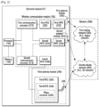
- FIG 1 illustrates an electronic device 101 in a network environment 100 according to an embodiment.
- the electronic device 101 in the network environment 100 may communicate with an electronic device 102 via a first network 198 (e.g., a short-range wireless communication network), or at least one of an electronic device 104 or a server 108 via a second network 199 (e.g., a long-range wireless communication network).
- a first network 198 e.g., a short-range wireless communication network
- a second network 199 e.g., a long-range wireless communication network
- the electronic device 101 may communicate with the electronic device 104 via the server 108.
- the electronic device 101 may include a processor 120, memory 130, an input module 150, a sound output module 155, a display module 160, an audio module 170, a sensor module 176, an interface 177, a connecting terminal 178, a haptic module 179, a camera module 180, a power management module 188, a battery 189, a communication module 190, a subscriber identification module (SIM) 196, or an antenna module 197.
- at least one of the components e.g., the connecting terminal 178) may be omitted from the electronic device 101, or one or more other components may be added in the electronic device 101.
- some of the components e.g., the sensor module 176, the camera module 180, or the antenna module 197) may be implemented as a single component (e.g., the display module 160).
- the processor 120 may execute, for example, software (e.g., a program 140) to control at least one other component (e.g., a hardware or software component) of the electronic device 101 coupled with the processor 120, and may perform various data processing or computation. According to one embodiment, as at least part of the data processing or computation, the processor 120 may store a command or data received from another component (e.g., the sensor module 176 or the communication module 190) in volatile memory 132, process the command or the data stored in the volatile memory 132, and store resulting data in non-volatile memory 134.
- software e.g., a program 140
- the processor 120 may store a command or data received from another component (e.g., the sensor module 176 or the communication module 190) in volatile memory 132, process the command or the data stored in the volatile memory 132, and store resulting data in non-volatile memory 134.
- the processor 120 may include a main processor 121 (e.g., a central processing unit (CPU) or an application processor (AP)), or an auxiliary processor 123 (e.g., a graphics processing unit (GPU), a neural processing unit (NPU), an image signal processor (ISP), a sensor hub processor, or a communication processor (CP)) that is operable independently from, or in conjunction with, the main processor 121.
- a main processor 121 e.g., a central processing unit (CPU) or an application processor (AP)
- auxiliary processor 123 e.g., a graphics processing unit (GPU), a neural processing unit (NPU), an image signal processor (ISP), a sensor hub processor, or a communication processor (CP)
- the main processor 121 may be adapted to consume less power than the main processor 121, or to be specific to a specified function.
- the auxiliary processor 123 may be implemented as separate from, or as part of the main processor 121.
- the auxiliary processor 123 may control at least some of functions or states related to at least one component (e.g., the display module 160, the sensor module 176, or the communication module 190) among the components of the electronic device 101, instead of the main processor 121 while the main processor 121 is in an inactive (e.g., sleep) state, or together with the main processor 121 while the main processor 121 is in an active state (e.g., executing an application).
- the auxiliary processor 123 e.g., an ISP or a CP
- the auxiliary processor 123 may include a hardware structure specified for artificial intelligence model processing.
- An artificial intelligence model may be generated by machine learning. Such learning may be performed, e.g., by the electronic device 101 where the artificial intelligence is performed or via a separate server (e.g., the server 108). Learning algorithms may include, but are not limited to, e.g., supervised learning, unsupervised learning, semi-supervised learning, or reinforcement learning.
- the artificial intelligence model may include a plurality of artificial neural network layers.
- the artificial neural network may be a deep neural network (DNN), a convolutional neural network (CNN), a recurrent neural network (RNN), a restricted Boltzmann machine (RBM), a deep belief network (DBN), a bidirectional recurrent deep neural network (BRDNN), deep Q-network or a combination of two or more thereof but is not limited thereto.
- the artificial intelligence model may, additionally or alternatively, include a software structure other than the hardware structure.
- the memory 130 may store various data used by at least one component (e.g., the processor 120 or the sensor module 176) of the electronic device 101.
- the various data may include, for example, software (e.g., the program 140) and input data or output data for a command related thereto.
- the memory 130 may include the volatile memory 132 or the non-volatile memory 134.
- the program 140 may be stored in the memory 130 as software, and may include, for example, an operating system (OS) 142, middleware 144, or an application 146.
- OS operating system
- middleware middleware
- application application
- the input module 150 may receive a command or data to be used by another component (e.g., the processor 120) of the electronic device 101, from the outside (e.g., a user) of the electronic device 101.
- the input module 150 may include, for example, a microphone, a mouse, a keyboard, a key (e.g., a button), or a digital pen (e.g., a stylus pen).
- the sound output module 155 may output sound signals to the outside of the electronic device 101.
- the sound output module 155 may include, for example, a speaker or a receiver.
- the speaker may be used for general purposes, such as playing multimedia or playing record.
- the receiver may be used for receiving incoming calls. According to an embodiment, the receiver may be implemented as separate from, or as part of the speaker.
- the display module 160 may visually provide information to the outside (e.g., a user) of the electronic device 101.
- the display module 160 may include, for example, a display, a hologram device, or a projector and control circuitry to control a corresponding one of the display, hologram device, and projector.
- the display module 160 may include a touch sensor adapted to detect a touch, or a pressure sensor adapted to measure the intensity of force incurred by the touch.
- a connecting terminal 178 may include a connector via which the electronic device 101 may be physically connected with the external electronic device (e.g., the electronic device 102).
- the connecting terminal 178 may include, for example, a HDMI connector, a USB connector, a SD card connector, or an audio connector (e.g., a headphone connector).
- the haptic module 179 may convert an electrical signal into a mechanical stimulus (e.g., a vibration or a movement) or electrical stimulus which may be recognized by a user via his tactile sensation or kinesthetic sensation.
- the haptic module 179 may include, for example, a motor, a piezoelectric element, or an electric stimulator.
- the power management module 188 may manage power supplied to the electronic device 101.
- the power management module 188 may be implemented as at least part of, for example, a power management integrated circuit (PMIC).
- PMIC power management integrated circuit
- the battery 189 may supply power to at least one component of the electronic device 101.
- the battery 189 may include, for example, a primary cell which is not rechargeable, a secondary cell which is rechargeable, or a fuel cell.
- the communication module 190 may support establishing a direct (e.g., wired) communication channel or a wireless communication channel between the electronic device 101 and the external electronic device (e.g., the electronic device 102, the electronic device 104, or the server 108) and performing communication via the established communication channel.
- the communication module 190 may include one or more CPs that are operable independently from the processor 120 (e.g., the AP) and supports a direct (e.g., wired) communication or a wireless communication.
- the communication module 190 may include a wireless communication module 192 (e.g., a cellular communication module, a short-range wireless communication module, or a global navigation satellite system (GNSS) communication module) or a wired communication module 194 (e.g., a local area network (LAN) communication module or a power line communication (PLC) module).
- a wireless communication module 192 e.g., a cellular communication module, a short-range wireless communication module, or a global navigation satellite system (GNSS) communication module
- GNSS global navigation satellite system
- wired communication module 194 e.g., a local area network (LAN) communication module or a power line communication (PLC) module.
- LAN local area network
- PLC power line communication
- a corresponding one of these communication modules may communicate with the external electronic device via the first network 198 (e.g., a short-range communication network, such as Bluetooth TM , wireless-fidelity (Wi-Fi) direct, or infrared data association (IrDA)) or the second network 199 (e.g., a long-range communication network, such as a legacy cellular network, a 5G network, a next-generation communication network, the Internet, or a computer network (e.g., LAN or wide area network (WAN)).
- first network 198 e.g., a short-range communication network, such as Bluetooth TM , wireless-fidelity (Wi-Fi) direct, or infrared data association (IrDA)
- the second network 199 e.g., a long-range communication network, such as a legacy cellular network, a 5G network, a next-generation communication network, the Internet, or a computer network (e.g., LAN or wide area network (WAN)).
- the wireless communication module 192 may identify and authenticate the electronic device 101 in a communication network, such as the first network 198 or the second network 199, using subscriber information (e.g., international mobile subscriber identity (IMSI)) stored in the subscriber identification module 196.
- subscriber information e.g., international mobile subscriber identity (IMSI)
- the wireless communication module 192 may support a 5G network, after a 4 th generation (4G) network, and next-generation communication technology, e.g., new radio (NR) access technology.
- the NR access technology may support enhanced mobile broadband (eMBB), massive machine type communications (mMTC), or ultra-reliable and low-latency communications (URLLC).
- eMBB enhanced mobile broadband
- mMTC massive machine type communications
- URLLC ultra-reliable and low-latency communications
- the wireless communication module 192 may support a high-frequency band (e.g., the mmWave band) to achieve, e.g., a high data transmission rate.
- the wireless communication module 192 may support various technologies for securing performance on a high-frequency band, such as, e.g., beamforming, massive multiple-input and multiple-output (massive MIMO), full dimensional MIMO (FD-MIMO), array antenna, analog beam-forming, or large scale antenna.
- the wireless communication module 192 may support various requirements specified in the electronic device 101, an external electronic device (e.g., the electronic device 104), or a network system (e.g., the second network 199).
- the wireless communication module 192 may support a peak data rate (e.g., 20Gbps or more) for implementing eMBB, loss coverage (e.g., 164dB or less) for implementing mMTC, or U-plane latency (e.g., 0.5ms or less for each of downlink (DL) and uplink (UL), or a round trip of 1ms or less) for implementing URLLC.
- a peak data rate e.g., 20Gbps or more
- loss coverage e.g., 164dB or less
- U-plane latency e.g., 0.5ms or less for each of downlink (DL) and uplink (UL), or a round trip of 1ms or less
- the antenna module 197 may transmit or receive a signal or power to or from the outside (e.g., the external electronic device) of the electronic device 101.
- the antenna module 197 may include an antenna including a radiating element composed of a conductive material or a conductive pattern formed in or on a substrate (e.g., a printed circuit board (PCB)).
- the antenna module 197 may include a plurality of antennas (e.g., array antennas). In such a case, at least one antenna appropriate for a communication scheme used in the communication network, such as the first network 198 or the second network 199, may be selected, for example, by the communication module 190 (e.g., the wireless communication module 192) from the plurality of antennas.
- the antenna module 197 may form a mmWave antenna module.
- the mmWave antenna module may include a printed circuit board, a RFIC disposed on a first surface (e.g., the bottom surface) of the printed circuit board, or adjacent to the first surface and capable of supporting a designated high-frequency band (e.g., the mmWave band), and a plurality of antennas (e.g., array antennas) disposed on a second surface (e.g., the top or a side surface) of the printed circuit board, or adjacent to the second surface and capable of transmitting or receiving signals of the designated high-frequency band.
- a RFIC disposed on a first surface (e.g., the bottom surface) of the printed circuit board, or adjacent to the first surface and capable of supporting a designated high-frequency band (e.g., the mmWave band)
- a plurality of antennas e.g., array antennas
- At least some of the above-described components may be coupled mutually and communicate signals (e.g., commands or data) therebetween via an inter-peripheral communication scheme (e.g., a bus, general purpose input and output (GPIO), serial peripheral interface (SPI), or mobile industry processor interface (MIPI)).
- an inter-peripheral communication scheme e.g., a bus, general purpose input and output (GPIO), serial peripheral interface (SPI), or mobile industry processor interface (MIPI)
- commands or data may be transmitted or received between the electronic device 101 and the external electronic device 104 via the server 108 coupled with the second network 199.
- Each of the electronic devices 102 or 104 may be a device of a same type as, or a different type, from the electronic device 101.
- all or some of operations to be executed at the electronic device 101 may be executed at one or more of the external electronic devices 102, 104, or 108. For example, if the electronic device 101 should perform a function or a service automatically, or in response to a request from a user or another device, the electronic device 101, instead of, or in addition to, executing the function or the service, may request the one or more external electronic devices to perform at least part of the function or the service.
- the one or more external electronic devices receiving the request may perform the at least part of the function or the service requested, or an additional function or an additional service related to the request, and transfer an outcome of the performing to the electronic device 101.
- the electronic device 101 may provide the outcome, with or without further processing of the outcome, as at least part of a reply to the request.
- a cloud computing, distributed computing, mobile edge computing (MEC), or client-server computing technology may be used, for example.
- the electronic device 101 may provide ultra low-latency services using, e.g., distributed computing or mobile edge computing.
- the external electronic device 104 may include an internet-of-things (IoT) device.
- the server 108 may be an intelligent server using machine learning and/or a neural network.
- the external electronic device 104 or the server 108 may be included in the second network 199.
- the electronic device 101 may be applied to intelligent services (e.g., smart home, smart city, smart car, or healthcare) based on 5G communication technology or IoT-related technology.
- the electronic device may be one of various types of electronic devices.
- the electronic devices may include, for example, a portable communication device (e.g., a smartphone), a computer device, a portable multimedia device, a portable medical device, a camera, a wearable device, or a home appliance. According to an embodiment of the disclosure, the electronic devices are not limited to those described above.
- each of such phrases as “A or B,” “at least one of A and B,” “at least one of A or B,” “A, B, or C,” “at least one of A, B, and C,” and “at least one of A, B, or C,” may include any one of, or all possible combinations of the items enumerated together in a corresponding one of the phrases.
- such terms as “1st” and “2nd,” or “first” and “second” may be used to simply distinguish a corresponding component from another, and does not limit the components in other aspect (e.g., importance or order).
- an element e.g., a first element
- the element may be coupled with the other element directly (e.g., wiredly), wirelessly, or via a third element.
- module may include a unit implemented in hardware, software, or firmware, and may interchangeably be used with other terms, for example, “logic,” “logic block,” “part,” or “circuitry”.
- a module may be a single integral component, or a minimum unit or part thereof, adapted to perform one or more functions.
- the module may be implemented in a form of an application-specific integrated circuit (ASIC).
- ASIC application-specific integrated circuit
- Various embodiments as set forth herein may be implemented as software (e.g., the program 140) including one or more instructions that are stored in a storage medium (e.g., internal memory 136 or external memory 138) that is readable by a machine (e.g., the electronic device 101).
- a processor e.g., the processor 120
- the machine e.g., the electronic device 101
- the one or more instructions may include a code generated by a complier or a code executable by an interpreter.
- the machine-readable storage medium may be provided in the form of a non-transitory storage medium.
- non-transitory simply means that the storage medium is a tangible device, and does not include a signal (e.g., an electromagnetic wave), but this term does not differentiate between where data is semi-permanently stored in the storage medium and where the data is temporarily stored in the storage medium.
- a method according to various embodiments of the disclosure may be included and provided in a computer program product.
- the computer program product may be traded as a product between a seller and a buyer.
- the computer program product may be distributed in the form of a machine-readable storage medium (e.g., compact disc read only memory (CD-ROM)), or be distributed (e.g., downloaded or uploaded) online via an application store (e.g., PlayStore TM ), or between two user devices (e.g., smart phones) directly. If distributed online, at least part of the computer program product may be temporarily generated or at least temporarily stored in the machine-readable storage medium, such as memory of the manufacturer's server, a server of the application store, or a relay server.
- CD-ROM compact disc read only memory
- an application store e.g., PlayStore TM
- two user devices e.g., smart phones
- each component e.g., a module or a program of the above-described components may include a single entity or multiple entities, and some of the multiple entities may be separately disposed in different components. According to various embodiments, one or more of the above-described components may be omitted, or one or more other components may be added. Alternatively or additionally, a plurality of components (e.g., modules or programs) may be integrated into a single component. In such a case, according to various embodiments, the integrated component may still perform one or more functions of each of the plurality of components in the same or similar manner as they are performed by a corresponding one of the plurality of components before the integration.
- operations performed by the module, the program, or another component may be carried out sequentially, in parallel, repeatedly, or heuristically, or one or more of the operations may be executed in a different order or omitted, or one or more other operations may be added.
- FIG 2 illustrates an electronic device in a network environment including a plurality of cellular networks according to an embodiment.
- an electronic device 101 includes a first CP (e.g., including processing circuitry) 212, a second CP (e.g., including processing circuitry) 214, a first RFIC 222, a second RFIC 224, a third RFIC 226, a fourth RFIC 228, a first radio frequency front end (RFFE) 232, a second RFFE 234, a first antenna module 242, a second antenna module 244, and an antenna 248.
- the electronic device 101 further includes a processor (e.g., including processing circuitry) 120 and a memory 130.
- the second network 199 includes a first cellular network 292 and a second cellular network 294.
- the first CP 212 can support establishment of a communication channel with a band to be used for wireless communication with the first cellular network 292 and legacy network communication through the established communication channel.
- the first cellular network may be a legacy network including a 2 nd generation (2G), 3 rd generation (3G), 4G, or Long-Term Evolution (LTE) network.
- the second CP 214 can support establishment of a communication channel corresponding to a designated band (e.g., about 6GHz ⁇ about 60GHz) of a band to be used for wireless communication with the second cellular network 294 and 5G network communication through the established communication channel.
- the second cellular network 294 may be a 5G network that is defined in 3 rd generation partnership project (3GPP).
- the first CP 212 or the second CP 214 can support establishment of a communication channel corresponding to another designated band (e.g., about 6GHz or less) of a band to be used for wireless communication with the second cellular network 294 and 5G network communication through the established communication channel.
- the first CP 212 and the second CP 214 may be implemented in a single chip or a single package.
- the first CP 212 or the second CP 214 may be disposed in a single chip or a single package together with the processor 120, the auxiliary processor 123, or the communication module 190.
- the first CP 212 and the second CP 214 is directly or indirectly connected by an interface, thereby being able to provide or receive data or control signal in one direction or two directions.
- the second RFIC 224 can convert a baseband signal generated by the first CP 212 or the second CP 214 into an RF signal in a Sub6 band (e.g., about 6GHz or less) (hereafter, 5G Sub6 RF signal) that is used for the second cellular network 294 (e.g., a 5G network).
- a 5G Sub6 RF signal can be obtained from the second cellular network 294 (e.g., a 5G network) through an antenna (e.g., the second antenna module 244) and can be preprocessed through an RFFE (e.g., the second RFFE 234).
- the second RFIC 224 can convert the processed 5G Sub6 RF signal into a baseband signal so that the processed 5G Sub6 RF signal can be processed by a corresponding CP of the first CP 212 or the second CP 214.
- the third RFIC 226 can convert a baseband signal generated by the second CP 214 into an RF signal in a 5G Above6 band (e.g., about 6GHz ⁇ about 60GHz) (hereafter, 5G Above6 RF signal) that is used for the second cellular network 294 (e.g., a 5G network).
- a 5G Above6 RF signal can be obtained from the second cellular network 294 (e.g., a 5G network) through an antenna (e.g., the antenna 248) and can be preprocessed through the third RFFE 236.
- a 5G Above6 RF signal can be received from the second cellular network 294 (e.g., a 5G network) through an antenna (e.g., the antenna 248) and can be converted into an IF signal by the third RFIC 226.
- the fourth RFIC 228 can covert the IF signal into a baseband signal so that IF signal can be processed by the second CP 214.
- the third RFIC 226 and the antenna 248 By disposing the third RFIC 226 and the antenna 248 on the same substrate, it is possible to reduce the length of the transmission line therebetween. Accordingly, it is possible to reduce a loss (e.g., attenuation) of a signal in a high-frequency band (e.g., about 6GHz ⁇ about 60 GHz), for example, which is used for 5G network communication, due to a transmission line. Accordingly, the electronic device 101 can improve the quality and the speed of communication with the second cellular network 294 (e.g., 5G network).
- a loss e.g., attenuation
- the electronic device 101 can access the access network of the 5G network and then can access an external network (e.g., the Internet) under control by the core network (e.g., an evolved packed core (EPC)) of the legacy network.
- EPC evolved packed core
- Protocol information e.g., LTE protocol information
- protocol information e.g., NR protocol information
- 5G network may be stored in the memory 230 and accessed by another part (e.g., the processor 120, the first CP 212, or the second CP 214).
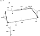
- the first surface 310A may be formed by a cover window 302 (e.g., a glass plate including various coating layers, or a polymer plate) which is substantially transparent at least in part.
- the cover window 302 may include a view area (VA) which is substantially transparent and/or a non-view area (N-VA) disposed to surround edges of the VA.
- VA view area
- N-VA non-view area
- the N-VA may be formed through a printing layer (or a black matrix (BM)) of a rear surface of the cover window 302, and the N-VA may be viewed in block from outside of the electronic device 300.
- the N-VA may be formed by opaquely coating one area of the cover window 302, or by coloring it with an opaque color.
- the second surface 310B may include a plurality of conductive portions 3103 and/or a plurality of nonconductive portions 3104 which segment the conductive portions 3103.
- the second surface 310B and the side surface 310C may be formed individually in their separate configuration.
- the second surface 310B may be formed by a rear plate, and the side surface 310C may be formed by a side surface bezel structure.
- the electronic device 300 may include at least one or more of a display 320, an audio module, camera modules 330 through 360, a key input device or a connector hole. Additionally, at least one of these components (e.g., the key input device) may be omitted from the electronic device 300 may omit, and/or the electronic device 300 may further include other components.
- the display 320 may be coupled with, or disposed adjacent to a touch sensing circuit, a pressure sensor for measuring a touch level (pressure), and/or a digitizer for detecting a stylus pen of a magnetic type.
- the audio module may include a microphone hole and a speaker hole.
- the microphone hole may include a microphone therein to acquire an external sound, and may include a plurality of microphones to detect a sound direction.
- the speaker hole may include a plurality of external speaker holes disposed in at least one area of the side surface 310C of the housing.
- the speaker hole may include four external speaker holes, but the number of the external speaker holes is not limited thereto.
- the speaker hole and the microphone hole may be implemented as a single hole, or a speaker (e.g., a piezo speaker) may be included without a speaker hole.
- the camera modules 330 through 360 may include the first camera 330 (or a front camera) disposed in the first surface 310A of the electronic device 300, the second camera 340 (or a first rear camera) disposed in the second surface 310B of the electronic device 300, the third camera 350 (or a second rear camera) and/or the flash 360 disposed in proximity to the second camera 340 and/or the third camera 350 disposed in the second surface 310B of the electronic device 300.
- the first camera 330 may be disposed in the rear surface of the N-VA of the cover window 302. At least part of the first camera 330 (e.g., a lens unit of the first camera 330) may be viewed in the first surface 310A of the electronic device 300 through a view portion of the N-VA.
- the view portion may indicate one area of the N-VA formed with a transparent material.
- the second camera 340, the third camera 350 and/or the flash 360 may be disposed in the nonconductive area 3102 of the second surface 310B.
- at least part of the second camera 340, the third camera 350 and/or the flash 360 e.g., one area of the second camera 340, the third camera 350 and/or the flash 360
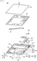
- FIG 4 illustrates an exploded view of an electronic device according to an embodiment.
- an electronic device 400 includes a frame 410, a cover window 420, a display 430, a flexible PCB (FPCB) 431, a PCB 440, a support member 450, a battery 460, a wireless charging coil 470, at least one magnet 480, at least camera module 490 and at least one antenna module 500.
- At least one of the components of the electronic device 400 may be identical or similar to at least one of the components of the electronic device of FIG 3A and FIG 3B , and redundant explanations shall be omitted.
- At least some of the components of the electronic device 400 e.g., the wireless charging coil 470 and/or the at least one magnet 480
- the wireless charging coil 470 and/or the at least one magnet 480 may be omitted, or other components may be added.
- the frame 410 includes a first structure 411 that forms a side surface and a rear surface of the electronic device 400 and/or a second structure 412 including at least one electronic component.
- the first structure 411 of the frame 410 includes a first surface 4111 that forms the side surface of the electronic device 400 and/or a second surface 4112 that is integrated with the first surface 4111 and forms the rear surface of the electronic device 400.
- the first surface 4111 of the first structure 411 may include a conductive portion 4111a and/or a nonconductive portion 4111B (or a segment portion) disposed at one end and the other end of the conductive portion 4111a to insulate the conductive portion 4111a.
- the conductive portion 4111a of the first structure 411 may be electrically connected with wireless communication circuity, to operate as an antenna radiator for transmitting and/or receiving an RF signal of a designated frequency band.
- At least one area of the second structure 412 of the frame 410 may include at least one electronic component for performing various functions of the electronic device 400.
- the PCB 440 and/or the battery 460 may be disposed on one surface (e.g., one surface in the +z direction of FIG 4 ) toward the display 430 of the second structure 412.
- the first structure 411 of the frame 410 may be disposed to surround edges of the second structure 412.
- the first structure 411 and the second structure 412 may be, but not limited to, integrally formed.
- the display 430 may be disposed below (e.g., in the -z direction of FIG 4 ) of the cover window 420, and may be visually exposed to outside of the electronic device 400 through a VA of the cover window 420.
- the display 430 may be visible in the front surface of the electronic device 400 through the cover window 420.
- the display 430 may be electrically connected with the PCB 440 through the FPCB 431.
- the PCB 440 may be interposed between the second structure 412 of the frame 410 and the support member 450, and the PCB 440 may include a processor, a memory, and/or an interface.
- the processor may include one or more of a CPU, an AP, a GPU, an ISP, a sensor hub processor, or a CP.
- the memory may include a volatile memory or a nonvolatile memory.
- the interface may include an HDMI, a USB interface, an SD card interface, and/or an audio interface.
- the interface may electrically or physically interconnect the electronic device 400 and an external electronic device, and may include a USB connector, an SD card/multimedia card (MMC) connector, or an audio connector.
- MMC Secure Digital
- the support member 450 may be disposed on the PCB 440 (e.g., in the +z direction), and may protect electronic components (e.g., the processor, the memory, and/or the interface) disposed on the PCB 440 and/or electronic components (e.g., the wireless charging coil 470 and/or the at least one magnet 480) disposed in the second structure 412 from an external shock or a foreign substance.
- the display 430 may be disposed in one surface (e.g., one surface in the +z direction) of the support member 450, and the PCB 440 may be disposed in the other surface (e.g., one surface in the -z direction) of the support member 450.
- the support member 450 may be a plate (or an injection-molded plate) formed with a nonconductive material, or the support member 450 may be a plate (or a metal plate) formed with a conductive material (e.g., a metal).
- the support member 450 may be spaced from the display 430, or may be attached to at least one area of the display 430.
- the battery 460 supplies power to at least one component of the electronic device 400, and may include a primary cell that is not rechargeable, a secondary cell that is rechargeable, or a fuel cell.
- the battery 460 may include at least one or more battery cells.
- the battery 460 may be a device that connects two battery cells in parallel. At least part of the battery 460 may be substantially flushed with the PCB 440. For example, at least part of the battery 460 may be disposed not to overlap the PCB 440 in one surface (e.g., one surface toward the +z direction) of the second structure 412. At least part of the battery 460 may be disposed to overlap some area of the PCB 440.
- the wireless charging coil 470 is interposed between the PCB 440 and the second structure 412 of the frame 410, and may wirelessly transmit and/or receive necessary power for charging an external electronic device.
- the wireless charging coil 470 may transmit the power to a stylus pen which is attachable to or detachable from the rear surface of the electronic device 400.
- the at least one magnet 480 may be interposed between the PCB 440 and the second structure 412 of the frame 410.
- the at least one magnet 480 includes a first magnet 481, a second magnet 482 and a third magnet 483.
- the first magnet 481, the second magnet 482, and/or the third magnet 483 may be magnetically coupled with magnets of the stylus pen, and accordingly the stylus pen may be mounted on the rear surface of the electronic device 400.
- a shield member may be disposed in an area adjacent to the first magnet 481, the second magnet 482, and/or the third magnet 483.
- the shield member may be disposed to surround the first magnet 481, the second magnet 482, and/or the third magnet 483, and thus obtain a distance between the first magnet 481 and the second magnet 482 and/or a distance between the second magnet 482 and the third magnet 483 over a designated distance.
- the shield member may obtain a distance between the first magnet 481 and the second magnet 482 and/or a distance between the second magnet 482 and the third magnet 483 over a designated distance, and thus reduce attraction and/or repulsion between the first magnet 481 and the second magnet 482 and/or between the second magnet 482 and the third magnet 483.
- At least one of the first magnet 481, the second magnet 482, or the third magnet 483 may be an array magnet including a plurality of magnets.
- the first magnet 481 near the wireless charging coil 470 may be an array magnet, and the first magnet 481 may prevent the stylus pen mounted in one area of the rear surface of the electronic device 400 from detaching from the electronic device 400 during the wireless charging.
- the at least one magnet 480 includes the first magnet 481, the second magnet 482, and the third magnet 483 in FIG 4 , the number of the magnets is not limited thereto.
- the at least one magnet 480 may include one magnet or a plurality of magnets (e.g., two, four, five, etc.).
- the at least one camera module 490 may be disposed in at least one area of the second structure 412 of the frame 410.
- the at least one camera module 490 may include a first camera module 491 and/or a second camera module 492.
- the first camera module 491 may be disposed toward the front surface (e.g., the +z direction) of the electronic device 400. At least part of the first camera module 491 may be visually exposed in the front surface of the electronic device 400 through some area (e.g., the view portion) of the cover window 420.
- the second camera module 492 may be disposed toward the rear surface (e.g., the -z direction) of the electronic device 400. At least part of the second camera module 492 (e.g., the lens unit of the camera) may be visually exposed in the rear surface of the electronic device 400 through a window area 4114a of the rear surface of the electronic device 400.
- the at least one antenna module 500 may include a plurality of antenna elements, and may be electrically connected with the wireless communication circuitry to transmit and/or receive an RF signal of a designated frequency band.
- the at least one antenna module 500 may transmit and/or receive an RF signal of a mmWave frequency band (e.g., about 28 GHz and/or about 39 GHz).
- the at least one antenna module 500 includes a first antenna module 510 and a second antenna module 520.
- the first antenna module 510 may be aligned in a horizontal direction (e.g., the +x direction or +y direction) based on the first camera module 491, and form a beam pattern toward the front direction (e.g., the +z direction) of the electronic device 400.
- the second antenna module 520 may be aligned in the horizontal direction (e.g., the +x direction or +y direction) based on the second camera module 492, and form a beam pattern toward the rear direction (e.g., the -z direction) of the electronic device 400.
- FIG 5 illustrates electrical connections of components of an electronic device according to an embodiment.
- an electronic device 400 includes a wireless charging coil 470, at least one magnet 480, a first camera module 491, a second camera module 492, at least one antenna module 500, and a processor 600.
- the at least one antenna module 500 may include an antenna array, an RFIC and/or a PMIC.
- the antenna array may include a plurality of antenna elements disposed to form a beam pattern.
- the RFIC may be electrically connected with a CP 610 and/or transceiver circuitry 611, and control a frequency and/or a phase of an RF signal.
- the PMIC may receive voltage from a PCB, and supply necessary power to an electronic component of the first antenna module 510 and/or the second antenna module 520 (e.g., an RFIC).
- the at least one antenna module 500 includes a first antenna module 510, and a second antenna module 520.
- the first antenna module 510 and the second camera module 491 may be aligned on a first virtual axis L 1 passing the first antenna module 510 and the first camera module 491.
- the first virtual axis L 1 may indicate a virtual line passing at least one area of the first antenna module 510 and at least one area of the first camera module 491.
- the second antenna module 520 and/or the second camera module 492 may be aligned on a second virtual axis L 2 passing the second antenna module 520 and the second camera module 492.
- the second virtual axis L 2 may indicate a virtual line passing at least one area of the second antenna module 520 and at least one area of the second camera module 492.
- the wireless charging coil 470 and/or the at least one magnet 480 may be also disposed on the second virtual axis L 2 .
- the first virtual axis L 1 and the second virtual axis L 2 may be in parallel.
- the first virtual axis L 1 and the second virtual axis L 2 may be the same axis, or the first virtual axis L 1 and the second virtual axis L 2 may be disposed substantially perpendicularly.
- the processor 600 includes a CP 610 and/or an AP 620.
- the CP 610 may be electrically connected with the first antenna module 510 and/or the second antenna module 520 through the transceiver circuitry 611.
- the CP 610 and/or the transceiver circuitry 611 may control the beam pattern generation of the first antenna module 510 and/or the second antenna module 520.
- the CP 610 may generate a baseband RF signal.
- the transceiver circuitry 611 may convert the baseband RF signal generated at the CP 610 into the mmWave frequency band (e.g., about 28 GHz or about 39 GHz), and generate the beam pattern by controlling a frequency and/or a phase of the first antenna module 510 and/or the second antenna module 520 based on the modulated RF signal.
- the transceiver circuitry 611 may convert the mmWave frequency band signal received from the external electronic device through the first antenna module 510 and/or the second antenna module 520 to a baseband signal to be processed at the CP 610.
- the transceiver circuitry 611 may convert a baseband signal to an RF signal of an intermediate frequency band (e.g., about 9 GHz through about 11 GHz) (hereafter, an IF signal) and then convert the IF signal to a mmWave frequency band signal, or convert a mmWave frequency band signal to an IF signal and then convert to a baseband signal.
- an intermediate frequency band e.g., about 9 GHz through about 11 GHz
- the AP 620 may be electrically connected with the first camera module 491 and/or the second camera module 492, and the AP 620 may control driving of the first camera module 491 and/or the second camera module 492.
- the AP 620 may be electrically connected with the wireless charging coil 470 through the wireless charging circuitry 621, to detect whether a stylus pen is attached or to control driving of the wireless charging coil 470. For example, a resonance signal or an induced magnetic field signal may generate between the electronic device 400 and the stylus pen.
- the electronic device 400 may receive a resonance signal or an induced magnetic field signal over a designated voltage (or a threshold voltage), and detect the attached stylus pen based on the received signal. If the stylus pen is detached from the electronic device 400, the electronic device 400 may receive a resonance signal or an induced magnetic field signal smaller than the designated voltage (or the threshold voltage), and detect the detached stylus pen based on the received signal. If the stylus pen is mounted (or attached) to the rear surface of the electronic device 400, the AP 620 may transmit and/or receive charging power and/or a communication signal including data through the wireless charging coil 470 and/or a coil of the stylus pen.
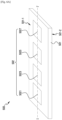
- an antenna module 500 includes a PCB 501, an antenna array 502, an RFIC 503, a PMIC 504, and a module interface.
- the antenna module 500 may further include a shield member 506.
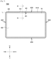
- the third area 4203 and/or the fourth area 4204 of the N-VA may be formed relatively longer than the first area 4201 and/or the second area 4202.
- a length ratio between the third area 4203 and/or the fourth area 4204 and the first area 4201 and/or the second area 4202 may be, but not limited to, 16:9 or 21:9.
- the first area 4201 and/or the second area 4202 of the N-VA may be formed relatively longer than the third area 4203 and/or the fourth area 4204.
- a plurality of conductive portions and/or a plurality of nonconductive portions which segment the conductive portions of a frame operating as an antenna radiator may be disposed on a rear surface of the first area 4201 and/or the second area 4202 of the N-VA.
- a first camera module 491 may be disposed in at least one area of the rear surface of the third area 4203 of the N-VA. At least one area of the third area 4203 may include a view portion 421, and at least part of the first camera module 491 may be viewed through the view portion 421 in the front surface of the electronic device 7000.
- the view portion 421 may be formed at a center of the third area 4203.
- the view portion 421 may be formed to lean in a left direction (e.g., the -x direction) based on the center of the third area 4203, or to lean in a right direction (e.g., the +x direction) based on the center of the third area 4203.
- Incident light from the front surface of the electronic device 7000 may be transmitted to the first camera module 491 through the view portion 421, and the first camera module 491 may obtain a field of view (FOV) toward the front surface of the electronic device 7000.
- FOV field of view
- the rear surface of the fourth area 4204 of the N-VA may include some area of an FPCB for electrically connecting the display 430 and a PCB disposed inside the electronic device 7000.
- the first antenna module 510 may be disposed in one area of the rear surface of the third area 4203 of the N-VA.
- the first antenna module 510 may be disposed on the rear surface of the third area 4203 of the N-VA, spaced from the first camera module 491 by a designated distance.
- the first antenna module 510 and the first camera module 491 may be aligned in the horizontal direction on a first virtual axis L 1 .
- the first virtual axis L 1 may indicate a virtual line passing one area of the first antenna module 510 and/or one area of the first camera module 491, and may be used hereafter with the same meaning.
- the first virtual axis L 1 may be in parallel to the +x axis, but the first virtual axis L 1 may be a line making a specific angle with the +x axis.
- the first antenna module 510 may be disposed on the rear surface of the N-VA, to form a beam pattern toward the front surface of the electronic device 7000 through the N-VA.
- the first antenna module 510 may transmit an RF signal of a designated frequency band to an external electronic device (, or receive an RF signal of the designated frequency band from the external electronic device.
- the designated frequency band may be about 28 GHz and/or about 39 GHz frequency band.
- the description of the electronic device 400 of FIG 4 may also be applied to the electronic device 7000.
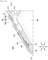
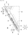
- FIG 8A illustrates an inside of the electronic device of FIG 7 , viewed from a front surface, according to an embodiment
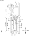
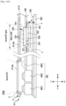
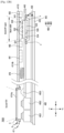
- FIG 8B illustrates a cross-sectional view of the electronic device of FIG 8A , taken along A - A', according to an embodiment
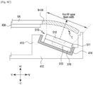
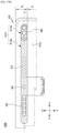
- FIG 8C illustrates a cross-sectional view of the electronic device of FIG 7 , taken along I - I', according to an embodiment.
- the electronic device 7000 includes a frame 410, a cover window 420, a display 430, a PCB, a support member 450, a first camera module 491, and a first antenna module 510.
- the frame 410 includes a first structure 411 and a second structure 412.
- the first structure 411 of the frame 410 may form a side surface and/or a rear surface of the electronic device 7000.
- the first structure 411 may be disposed to surround edges of the second structure 412, or the first structure 411 and the second structure 412 may be integrally formed.
- the second structure 412 of the frame 410 may include at least one electronic component, and the second structure 412 may support the at least one electronic component.
- the PCB 440, the first camera module 491, and/or the first antenna module 510 may be disposed on one surface toward the +z direction of the second structure 412.
- the PCB 440 may be disposed in at least part of an area (an area A) corresponding to a VA of the cover window 420 of the second structure 412 and/or an area (an area B) corresponding to an N-VA of the cover window 420.
- the first camera module 491 and/or the first antenna module 510 may be disposed in the area (the area B) corresponding to the N-VA of the cover window 420.
- the first antenna module 510 may be spaced from the first camera module 491 by a designated distance.
- the first camera module 491 and/or the first antenna module 510 may be aligned in the horizontal direction (e.g., the +x direction) on a first virtual axis L 1 .
- the first camera module 491 may be disposed in an area corresponding to a view portion 421 of the N-VA of the cover window. For example, when viewed from above (e.g., the +z direction) of the cover window 420, the view portion 421 of the cover window 420 and at least one area of the first camera module 491 may be overlapped. The first camera module 491 may obtain a first FOV toward the front direction (e.g., the +z direction) of the electronic device 7000 through the view portion 421.
- the first antenna module 510 includes a first PCB 511, a first antenna array 512, and/or a first RFIC 513.
- the first antenna array 512 may be disposed in one surface (e.g., one surface of the +z direction) toward the cover window 420 of the first PCB 511, and the first RFIC 513 may be disposed in one surface (e.g., one surface of the -z direction) toward the second structure 412 of the first PCB 511.
- the first antenna array 512 may be disposed in one surface toward the cover window 420 of the first PCB 511, to operate as a radiator which forms a beam pattern toward the cover window 420 (e.g., +z direction).
- the first RFIC 513 may be packaged in one surface toward the second structure 412 of the first PCB 511 by a first shield member 516, and the first shield member 516 may electromagnetically shield the first RFIC 513.
- the first shield member 516 may be formed with an epoxy material.
- the first antenna module 510 may be electrically connected with the PCB 440 through the first FPCB 514.
- the first RFIC 513 of the first antenna module 510 may be electrically connected with wireless communication circuitry disposed on the PCB 440 through the first FPCB 514.
- the wireless communication circuitry may control an angle of the beam pattern generated at the first antenna array 512, by controlling a phase and/or a frequency of the RF signal generated at the first antenna array 512 through the first RFIC 513.
- the first antenna module 510 may generate a first RF signal toward the cover window 420 through the first antenna array 512 and/or the first RFIC 513.
- the first antenna module 510 may generate the first RF signal toward substantially the same direction as the first FOV of the first camera module 491.
- the first antenna module 510 may be tilted a specific angle toward the side surface based on the front surface of the electronic device 7000.
- the first antenna module 510 may be tilted the specific angle toward the +y axis based on the +z axis.
- a radiation surface of the first antenna module 510 may be disposed at a position corresponding to a curved area C (or an edge area) of the N-VA of the cover window 420.
- the curved area C of the N-VA may indicate a curved area toward the side surface from the front surface of the electronic device 7000.
- the first antenna module 510 may form a beam pattern toward one direction between the +z axis and the +y axis in the above-described structure.
- the second structure 412 of the frame 410 may include a support structure 413 protruding toward the cover window 420 (e.g., in the +z direction) in at least one area of the second structure 412, and receiving the first antenna module 510.
- the support structure 413 may be formed in at least one area of the area (the area B) corresponding to the N-VA of the cover window 420 of the second structure 412, and may include a body portion 4131 and/or a protruding portion 4132.
- the first antenna module 510 may be disposed in at least one area of one surface (e.g., one surface toward the +z direction) toward the cover window 420 of the body portion 4131.
- the protruding portion 4132 may be disposed in at least one edge of the body portion 4131, and may protrude toward the cover window 420 in the body portion 4131.
- the body portion 4131 and/or the protruding portion 4132 disposed in at least one edge of the body portion 4131 may form a recess in one surface toward the cover window 420 of the support structure 413.
- the first antenna module 510 may be disposed in the recess, and supported by the support member 413.
- the support member 413 may include an insulating member 414 formed with a nonconductive material (e.g., plastic) and interposed between the first antenna module 510 and the support structure 413.
- the insulating member 414 may be disposed inside the recess of the support structure 413 formed by the body portion 4131 and/or the protruding portion 4132.
- the insulating member 414 may be disposed in at least one area of one surface toward the cover window 420 of the body portion 4131 and/or at least one area of an inner side surface of the protruding portion 4132.
- the insulating member 414 may prevent current leaked from the first antenna module 510 (hereafter, referred to as leakage current) from flowing into the second structure 412 formed with a conductive material (e.g., a metal), thus preventing a user from being electrocuted by the leakage current.
- leakage current current leaked from the first antenna module 510
- a conductive material e.g., a metal
- the support member 413 may be formed lower in height than the first antenna module 510.
- the first antenna module 510 may be formed with first height hi based on the body portion 4131 of the support structure 413.
- the protruding portion 4132 may be formed with second height h 2 lower than the first height h 1 based on the body portion 4131, and a gap may be formed between the first antenna module 510 and the protruding portion 4132.
- a difference of the height h 1 of the first antenna module 510 and the height h 2 of the protruding portion 4132 may be about 0.4 mm, and the gap may be formed between the first antenna module 510 and the protruding portion 4132 due to the height difference of the first antenna module 510 and the protruding portion 4132.
- the height difference of the first antenna module 510 and the protruding portion 4132 is not limited to the example above.
- the protruding portion 4132 may interfere with the beam pattern formed at the first antenna module 510.
- the protruding portion 4132 may interfere the beam pattern formed toward the +x direction or the -x direction of the first antenna module 510.
- the electronic device 7000 may reduce the interference of the support structure 413 in the beam pattern radiated from the first antenna module 510.
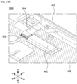
- FIG 9A illustrates a partial area, without a display panel, in the electronic device of FIG 7 according to an embodiment
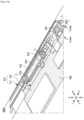
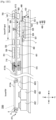
- FIG 9B illustrates a cross-sectional view of the electronic device of FIG 9A , taken along B - B', according to an embodiment.
- FIG 9A illustrates an inside of the electronic device, 7000 without a cover window and a display on the front surface (e.g., in the +z direction).
- the electronic device 7000 includes a frame 410, a first support frame 415, a cover window 420, a PCB 440, a support member 450, a first camera module 491, and/or a first antenna module 510.
- the frame 410 includes a first structure 411 and/or a second structure 412.
- the first structure 411 of the frame 410 may form a side surface and/or a rear surface of the electronic device 7000.
- the first structure 411 may be disposed to surround edges of the second structure 412.
- the first structure 411 and the second structure 412 may be integrally formed.
- the second structure 412 of the frame 410 may include at least one electronic component, and the second structure 412 may support the at least one electronic component.
- the PCB 440, the first camera module 491, and/or the first antenna module 510 may be disposed in one surface toward the +z direction of the second structure 412.
- the PCB 440 may be disposed in an area (an area A) corresponding to a VA of the cover window 420 of the second structure 412 and/or at least part of an area (an area B) corresponding to an N-VA of the cover window 420.
- the first camera module 491 and/or the first antenna module 510 may be disposed in the area (the area B) corresponding to the N-VA of the cover window 420.
- the first antenna module 510 may be spaced from the first camera module 491 by a designated distance.
- the first camera module 491 and/or the first antenna module 510 may be aligned in the horizontal direction (e.g., the +x direction) on a first virtual axis L 1 .
- the first camera module 491 may be disposed in an area corresponding to a view portion 421 of the N-VA of the cover window. For example, when viewed from above (e.g., in the +z direction) of the cover window 420, the view portion 421 of the cover window 420 and at least one area of the first camera module 491 may be overlapped. The first camera module 491 may obtain a first FOV toward a front direction (e.g., the +z direction) of the electronic device 7000 through the view portion 421.
- a front direction e.g., the +z direction
- the first antenna module 510 may include a first PCB 511, a first antenna array 512, and/or a first RFIC 513.
- the first antenna array 512 may be disposed in one surface (e.g., one surface of the +z direction) toward the cover window 420 of the first PCB 511, and the first RFIC 513 may be disposed in one surface (e.g., one surface of the -z direction) toward the second structure 412 of the first PCB 511.
- the first RFIC 513 may be packaged in one surface toward the second structure 412 of the first PCB 511 by a first shield member 516, and the first shield member 516 may electromagnetically shield the first RFIC 513.
- the first shield member 516 may be formed with an epoxy material.
- the first antenna array 512 may be disposed in one surface toward the cover window 420 of the first PCB 511, to operate as a radiator which forms a beam pattern toward the cover window 420 (e.g., the +z direction).
- the first antenna module 510 may be electrically connected with the PCB 440 through the first FPCB 514.
- the first RFIC 513 of the first antenna module 510 may be electrically connected with wireless communication circuitry disposed on the PCB 440 through the first FPCB 514.
- the wireless communication circuitry may control an angle of the beam pattern generated at the first antenna array 512, by controlling a phase and/or a frequency of an RF signal generated at the first antenna array 512 through the first RFIC 513.
- the first antenna module 510 may generate a first RF signal toward the cover window 420 through the first antenna array 512 and/or the first RFIC 513.
- the first antenna module 510 may generate the first RF signal toward substantially the same direction as the first FOV of the first camera module 491.
- the second structure 412 of the frame 410 includes a support structure 413 protruding toward the cover window 420 (e.g., the +z direction) in at least one area of the second structure 412.
- the support structure 413 may be formed in at least one area of the area (the area B) corresponding to the N-VA of the cover window 420 of the second structure 412, and may include a body portion 4131 and/or a protruding portion 4132.
- the first antenna module 510 may be disposed in at least one area of one surface (e.g., one surface toward the +z direction) toward the cover window 420 of the body portion 4131.
- the protruding portion 4132 may be disposed in at least one edge of the body portion 4131, and may protrude toward the cover window 420 in the body portion 4131.
- the body portion 4131 and/or the protruding portion 4132 disposed in at least one edge of the body portion 4131 may form a recess in one surface toward the cover window 420 of the support structure 413.
- the support member 413 may include an insulating member 414 formed with a nonconductive material (e.g., plastic) and interposed between the first antenna module 510 and the support structure 413.
- the insulating member 414 may be disposed inside the recess of the support structure 413 formed by the body portion 4131 and/or the protruding portion 4132.
- the insulating member 414 may be disposed in at least one area of one surface toward the cover window 420 of the body portion 4131 and/or at least one area of an inner side surface of the protruding portion 4132.
- the first support frame 415 may be disposed in the recess of the support member 415, to support the first antenna module 510.
- the first support frame 415 may be disposed within the recess and/or in at least one area of one surface toward the cover window 420 of the protruding portion 4132.
- the first support frame 415 may be disposed on (e.g., in the +z direction) of the insulating member 414 of the support structure 413.
- the first support frame 415 may be secured to the protruding portion 4132 using a screw S.
- a screw hole may be formed in an area corresponding to the protruding portion 4132 of the first support frame 415.
- the screw S is fastened between the first support frame 415 and the protruding portion 4132 through the screw hole, and thus, the first support frame 415 may be secured to at least one area (e.g., the protruding portion 4132) of the support structure 413.
- the first antenna module 510 may be attached to at least one area of the first support frame 415.
- An adhesive member may be disposed between the first antenna module 510 and one surface toward the cover window 420 of the first support frame 415, and the first antenna module 510 may be attached to at least one area of the first support frame 415 using the adhesive member.
- the adhesive member may be an adhesive tape including a thermally conductive sheet.
- the first support frame 415 may be formed of a conductive material (e.g., a metal), to support the first antenna module 510 and also radiate heat generated from the first antenna module 510. Excessive heat may generate if the first antenna module 510 generates the RF signal, and this heat may cause performance degradation of the first antenna module 510. Accordingly, the first support frame 415 may include a working fluid therein, and may be formed in a vapor chamber structure for radiating the heat from the first antenna module 510 using phase change of the working fluid.
- a conductive material e.g., a metal
- the first support frame 415 may transfer the heat from the first antenna module 510 to the frame 410, by contacting at least part (e.g., the first RFIC 513) of the first antenna module 510.
- the heat generated from the first antenna module 510 may be transferred to the second structure 412 of the frame 410 through the first support frame 415 and/or the screw S, which secures the first support frame 415 and the support frame 413, and the first support frame 415 may radiate the heat generating from the first antenna module 510 through this heat transfer.
- a groove G 1 may be formed in at least one area of the insulating member 414 in which the first support frame 415 is disposed, to form an air gap between the first support frame 415 and the insulating member 414.
- the air gap between the insulating member 414 and the first support frame 415 may provide a space for radiating the heat generated from the first antenna module 510.
- the air gap between the insulating member 414 and the first support frame 415 may prevent hot spot in one area of the second structure 412 of the frame 410.
- heat diffusion through the first support frame 415 may be faster than heat diffusion through the air gap between the insulating member 414 and the first support frame 415, and the air gap may prevent the hot spot in one area of the second structure 412 using the heat diffusion difference.
- the support member 413 may be formed to be lower in height than the first antenna module 510.
- the first antenna module 510 may be formed with first height h 1 based on the body portion 4131 of the support structure 413.
- the protruding portion 4132 may be formed with second height h 2 based on the body portion 4131, and the first support frame 214 disposed on the protruding portion 4132 may have third height h 3 .
- the first height h 1 may be greater than a sum of the second height h 2 and the third height h 3 , and accordingly, a gap may be formed between the first antenna module 510 and the first support frame 415 disposed on the protruding portion 4132.
- the first antenna module 510 and the first support frame 415 may have the gap of about 0.4 mm.
- the protruding portion 4132 and/or the first support frame 415 may interfere a beam pattern generated at the first antenna module 510.
- the protruding portion 4132 and/or the first support frame 415 may prevent the beam pattern formed toward the +x direction or the -x direction.
- An area of the screw S e.g., a head area of the screw S
- a gap of about 1.4 mm may be formed between the head area of the screw S and the one surface toward the +z direction of the first antenna module 510.
- the screw S may be positioned out of a beam width of a first RF signal generated at the first antenna module 510. Even if the some area of the screw S (e.g., the head area of the screw S) is formed higher than the first antenna module 510, the beam pattern generation of the first antenna module 510 may not be interfered based on the above-described structure.
- the electronic device 7000 may reduce the interference of the protruding portion 4132 of the support structure 413 and/or the first support frame 415 in the beam pattern radiated from the first antenna module 510.
- FIG 10 illustrates a rear surface of an electronic device according to an embodiment.
- the electronic device 7000 includes a frame 410, a second camera module 492, and a second antenna module 520. At least one of the components of the electronic device 7000 may be identical to similar to at least one of the components of the above-described electronic devices 7000, and redundant explanations shall be omitted.
- the frame 410 includes a first structure 411 which forms a side surface and/or a rear surface of the electronic device 7000. At least one surface of the first surface 411 which forms the side surface of the electronic device 7000 includes a plurality of conductive portions 4111a and a plurality of nonconductive portions 4111b for insulating the conductive portions 4111a.
- the conductive portions 4111a and the nonconductive portions 4111b may be disposed in a left area (e.g., the +x direction) and/or a right area (e.g., the -x direction) of the electronic device 7000.
- the conductive portions 4111a of the first structure 411 may be electrically connected with wireless communication circuitry disposed on a PCB and/or a ground of the PCB.
- the conductive portions 4111a may operate as an antenna radiator (e.g., an inverted F antenna (IFA)) for transmitting and/or receiving the RF signal of the designated frequency band using the electrical connection.
- IFA inverted F antenna
- a surface of the first structure 411 that forms the rear surface of the electronic device 7000 may include a conductive area 4113 formed with a conductive material (e.g., a metal) and/or a nonconductive area 4114 formed at least in part with a nonconductive material (e.g., a polymer).
- a conductive material e.g., a metal
- a nonconductive area 4114 formed at least in part with a nonconductive material (e.g., a polymer).
- the nonconductive area 4114 may include a window area 4114a and/or a nonconductive member 4114b formed with a nonconductive material (e.g., a polymer).
- the window area 4114a may be formed at a position corresponding to at least part of the second camera module 492, and formed at least in part with a transparent material. At least part of the second camera module 492 is visible in the rear surface of the electronic device 7000.
- the window area 4114a may include a decoration member D disposed to surround at least one area of edges of the window area 4114a and/or an enclosure E disposed between the window area 4114a and the decoration member D.
- the decoration member D may be formed with a glass material or a plastic material.
- a slot extending along the +x direction based on the window area 4114a may be formed in one surface of the first structure 411, which forms the rear surface of the electronic device 7000.
- the nonconductive member 4114b may be disposed within the slot, to form at least part of the rear surface of the electronic device 7000.
- the second camera module 492 may be disposed in an area corresponding to the window area 4114a of the nonconductive area 4114 of the electronic device 7000. When viewed from the rear surface of the electronic device 7000, at least one area of the second camera module 492 may be disposed to overlap the window area 4114a.
- the second camera module 492 may include a 2-1 camera 4921 (, a 2-2 camera 4922, and/or a flash 4923. At least part of the 2-1 camera 4921, the 2-2 camera 4922, and/or the flash 4923 (e.g., some area of lens portions of the 2-1 camera 4921, the 2-2 camera 4922, and/or the flash 4923) may be visually exposed in the rear surface of the electronic device 7000 through the window area 4114a.
- the second antenna module 520 may be disposed in an area corresponding at least in part to one portion of the nonconductive member 4114b of the nonconductive area 4114 of the electronic device 7000. For example, when viewed from the rear surface of the electronic device 7000, the second antenna module 520 may be disposed to overlap one portion of the nonconductive member 4114b.
- the second antenna module 520 may be spaced from the second camera module 492.
- the second antenna module 520 and the second camera module 492 may be aligned in the horizontal direction (e.g., the +x direction) on a second virtual axis L 2 .
- the second virtual axis L 2 may indicate a virtual line passing at least one area of the second antenna module 520 and/or at least one area of the second camera module 492, and may be used hereafter with the same meaning.
- the second virtual axis L 2 may be in parallel to the +x axis, but the second virtual axis L 2 may be a line making a specific angle with the +x axis according to an embodiment.
- the second antenna module 520 may be disposed in an area corresponding to one portion of the nonconductive member 4114b, to form a beam pattern toward the rear surface of the electronic device.
- the second antenna module 520 may transmit an RF signal of a designated frequency band to an external electronic device, or receive an RF signal of the designated frequency band from the external electronic device.
- the designated frequency band may be about 28 GHz and/or about 39 GHz frequency band.
- FIG 11A illustrates an inside of the electronic device of FIG 10 , viewed from the rear surface, according to an embodiment
- FIG 11B illustrates a second antenna module of FIG 11A , viewed from the front surface of the electronic device
- FIG 11C illustrates a cross-sectional view of the electronic device of FIG 11A , taken along C - C'.
- some of the rear area of the electronic device 7000 is removed in FIG 11A
- the second antenna module 520 of FIG 11A is viewed in the +z direction in FIG 11B
- the second structure 412 of the frame 410 is omitted in the electronic device 7000 of FIG 11C
- the electronic device 7000 includes a frame 410, a cover window 420, a display 430, a PCB 440, a battery 460, a first camera module 491, a second camera module 492, a first antenna module 510, and/or a second antenna module 520. At least one of the components of the electronic device 7000 may be identical to or similar to at least one of the components of the above-described electronic devices, and redundant explanations shall be omitted.
- the frame 410 includes a first structure 411 and/or a second structure 412.
- the first structure 411 may be formed at edges of the second structure 412, and the first structure 411 and the second structure 412 may be integrally formed.
- the first structure 411 of the frame 410 may form a side surface and/or a rear surface of the electronic device 411.
- a surface of the first structure 411 that forms the rear surface of the electronic device 7000 may include a nonconductive area 4114 and/or a conductive area disposed to surround the nonconductive area 4114.
- the nonconductive area 4114 includes a window area 4114a allowing at least part of the second camera module 492 to be viewed in the rear surface of the electronic device 7000 and/or a nonconductive member 4114b extending along the +x direction based on the window area 4114a.
- the window area 4114a may further include a decoration member D surrounding at least part of edges of the window area 4114a and/or an enclosure E disposed between the window area 4114a and the decoration member D.
- the nonconductive member 4114b may be formed with a nonconductive material (e.g., a polymer), to form part of the rear surface of the electronic device 7000.
- the second structure 412 of the frame 410 may include at least one electronic component.
- the PCB 440, the battery 460, the first camera module 491, the second camera module 492 and/or the first antenna module 510 may be disposed in one surface toward the +z direction of the second structure 412.
- the PCB 440 may be disposed not to overlap the battery 460 in one surface toward the +z direction of the second structure 412.
- the first camera module 491 and the first antenna module 510 may be aligned in the horizontal direction (e.g., the +x direction) on a first virtual axis L 1 .
- the second camera module 492 may be disposed in one area of the second structure 412 corresponding to a window area 4114a of the first structure 411. For example, when viewed from the rear surface (e.g., the -z direction) of the electronic device 7000, the second camera module 492 may be disposed to overlap at least one area of the window area 4114a.
- the second camera module 492 may include a 2-1 camera 4921, a 2-2 camera 4922, and/or a flash 4923. Incident light from the rear surface of the electronic device 7000 through the window area 4114a may be transmitted to the 2-1 camera 4921 and/or the 2-2 camera 4922.
- the 2-1 camera 4921 and/or the 2-2 camera 4922 may obtain a second FOV toward the rear surface (e.g., the -z direction of FIG 11C ) of the electronic device 7000 through the window area 4114a.
- the second antenna module 520 may be disposed in one area of the PCB 440 corresponding to the nonconductive member 4114b.
- the second antenna module 520 may be disposed in one area of the PCB 440 overlapping the nonconductive member 4114b, when viewed from the rear surface of the electronic device 7000.
- At least one area of the PCB 440 corresponding to the nonconductive member 4114b may include a through hole 441, and the second antenna module 520 may be disposed inside the through hole 441.
- the second antenna module 520 may be disposed in parallel with the second camera module 492.
- the second antenna module 520 and the second camera module 492 may be aligned in the horizontal direction (e.g., the +x direction) on a second virtual axis L 2 passing centers of the second antenna module 520 and the second camera module 492.
- the PCB 440 may include a second support frame 442 disposed near the through hole 441 and supporting the second antenna module 520 in the through hole 441.
- the second support frame 442 may be coupled (or secured) to one area of one surface (e.g., one surface toward the +z direction) toward the cover window 420 of the PCB 440, and support at least one area of the second antenna module 520 in the through hole 441.
- the second support frame 442 may be secured to the area adjacent to the through hole 441 in the one surface of the PCB 440.
- the second support frame 442 may surround at least part of the second antenna module 520, and support at least one area of the second antenna module 520.
- the second support frame 442 may be surface-mounted on one surface toward the cover window 420 of the PCB 440.
- the second support frame 442 may be coupled (or soldered) to the one area (e.g., the one surface toward the +z direction) of the PCB 440 through solder pads S 1 and S 2 disposed in the one surface toward the cover window 420 of the PCB 440.
- the second support frame 442 may be formed of a conductive material (e.g., a metal), to secure the second antenna module 520 and also shield noise introduced to the second antenna module 520.
- the solder pads S 1 and S 2 interposed between the second support frame 442 and the PCB 440 may be electrically connected to a ground of the PCB 440.
- the second support frame 442 may be electrically connected with the ground of the PCB 440.
- the second support frame 442 may operate as the ground through this electrical connection, and thus, the second support frame 442 shield the noise introduced to the second antenna module 520.
- the second support frame 442 may be spaced from the display 430, which is disposed on the +z direction of the second support frame 442, by a designated distance (e.g., G 2 of FIG 11C ), and form a structure for radiating heat generating from the second antenna module 520. For example, excessive heat may be generated if the second antenna module 520 transmits and/or receives an RF signal of a designated frequency, and the generated heat may be transferred to the second support frame 442 formed with the conductive material. Since the second support frame 442 is spaced from the display 430 by the designated distance G 2 , an air gap may be formed between the second support frame 442 and the display 430. The air gap generated between the second support frame 442 and the display 430 may cool the extreme heat transferred to the second support frame 442, and thus, the heat generated in operating the second antenna module 520 may be radiated.
- a designated distance e.g., G 2 of FIG 11C
- the second support frame 442 may include a working fluid therein, and may be formed in a vapor chamber structure for radiating the heat from the second antenna module 520 using phase change of the working fluid.
- the electronic device 7000 may further include a heat radiating member attached to the second support frame 442 and/or the second antenna module 520.
- the heat radiating member which is interposed between the second support frame 442 and the second antenna module 520, may more effectively radiate the heat generated if the second antenna module 520 transmits and/or receives the RF signal of the designated frequency.
- the heat radiating member which is formed with a nonconductive material having good radiation characteristics, may prevent leakage current generated at the second antenna module 520 from flowing to the frame 410 through the second support frame 442.
- the heat radiating member may include a plate formed with a good heat radiation material, a heat radiation tape, or graphite.
- a recess (or a groove) may be formed in at least one area of the PCB 440 corresponding to the nonconductive member 4114b, and the second antenna module 520 may be disposed in the recess of the PCB 440.
- the second antenna module 520 may be disposed directly in at least one area (e.g., one surface toward the -z direction) of the PCB 440 corresponding to the nonconductive member 4114b.
- the second antenna module 520 may include a second PCB 521, a second antenna array 522, and/or a second RFIC 523.
- the second antenna array 522 may be disposed in the rear surface 7000 of the second PCB 521 or one surface (e.g., one surface toward the -z direction) toward the nonconductive member 4114B.
- the second antenna array 522 may be disposed in one surface of the second PCB 521 toward the rear surface of the electronic device 7000, operating as a radiator that forms a beam pattern toward the rear surface (e.g., the -z direction) of the electronic device 7000.
- the second RFIC 523 may be disposed in the front surface of the electronic device 7000 or one surface (e.g., one surface toward the +z direction) of the second PCB 521 toward the cover window 420.
- the second RFIC 523 may be packaged in one surface toward of the second PCB 521 the cover window 420 by a second shield member 526, and the second shield member 526 may electromagnetically shield the second RFIC 523.
- the second shield member 526 may be formed with an epoxy material.
- the second antenna module 520 may be electrically connected with the PCB 440 through the second FPCB 524.
- the second antenna module 520 may be electrically connected with wireless communication circuitry disposed on the PCB 440 through the second FPCB 524.
- the wireless communication circuitry may be electrically connected with the second RFIC 523 of the second antenna module 520.
- the wireless communication circuitry may control an angle of the beam pattern generated at the second antenna array 522, by controlling a phase and/or a frequency of an RF signal generated at the second antenna array 522.
- the second antenna module 520 may generate a second RF signal toward the second antenna array 522 and/or the rear surface (e.g., the -z direction) of the electronic device 7000 through the second RFIC 523.
- the second antenna module 520 may generate the second RF signal toward substantially the same direction as the second FOV of the second camera module 492. If a conductive material is disposed in the radiation direction of the RF signal, the conductive material may cause radiation performance degradation of the antenna (e.g., the second antenna module 520).
- the electronic device 7000 may reduce the radiation performance degradation of the second antenna module 520, by disposing the nonconductive member 4114b formed with the nonconductive material in the beam pattern direction of the second antenna array 522.
- FIG 12A illustrates an inside of the electronic device of FIG 10 , viewed from the rear surface, according to an embodiment
- FIG 12B illustrates a cross-sectional view of the electronic device of FIG 12A , taken along D - D', according to an embodiment
- FIG 12C illustrates a cross-sectional view of the electronic device of FIG 12B with a stylus pen, according to an embodiment.
- some of the rear area of the electronic device 7000 is removed in FIG 12A
- FIG 12B and/or FIG 12C are the cross-sectional views of the electronic device 7000 with a second structure 412 of a frame 410 omitted.
- the electronic device 7000 includes a frame 410, a cover window 420, a display 430, a PCB 440, a battery 460, a wireless charging coil 470, at least one magnet 480, a first camera module 491, a second camera module 492, a first antenna module 510, and/or a second antenna module 520.
- the electronic device 7000 in FIGs. 12A , 12B , and 12C similar to the electronic device of FIGs. 11A , 11B and/or 11C, but adds the wireless charging coil 470 and/or the at least one magnet 480. Accordingly, redundant explanations shall be omitted.
- the wireless charging coil 470 and/or the at least one magnet 480 may be disposed in the rear surface of the electronic device 7000 on the PCB 440 or a surface (e.g., one surface toward the - z direction) toward a nonconductive area 4114 of the frame 410.
- the wireless charging coil 470 and/or the at least one magnet 480 may be disposed on the one surface of the PCB 440 overlapping a nonconductive member 4114b of the nonconductive area 4114.
- the wireless charging coil 470 and/or the at least one magnet 480 may be disposed in parallel with the second camera module 492 and the second antenna module 520
- the wireless charging coil 470, the at least one magnet 480, the second camera module 492, and/or the second antenna module 520 may be aligned in the horizontal direction (e.g., the +x direction) on a second virtual axis L 2 passing centers of the second antenna module 520 and the second camera module 492.
- the wireless charging coil 470 may be spaced from the second camera module 482 by a designated distance, and wirelessly charge an electronic component disposed on the nonconductive member 4114b of the rear surface of the electronic device 7000.
- the wireless charging coil 470 may wirelessly charge a battery of a stylus pen 700 attachable to and detachable from the nonconductive member 4114b of the electronic device 7000.
- the wireless charging coil 470 may be electrically connected with a processor disposed on the PCB 440, and the processor may control the wireless charging coil 470.
- a resonance signal or an induced magnetic field signal M may be generated between the electronic device 7000 and the stylus pen 700. If the stylus pen 700 is fixed in one area of the nonconductive member 4114b by means of magnets 701, 702, and 703 of the stylus pen 700, the electronic device 7000 may receive the resonance signal or the induced magnetic field signal M over a designated voltage (or a threshold voltage), and detect that the stylus pen 700 is attached to the nonconductive member 4114b based on the received signal M.
- the wireless charging coil 470 is a wound coil of a solenoid type in FIG 12B and FIG 12C
- the structure of the wireless charging coil 470 is not limited thereto.
- the wireless charging coil 470 may be a coil of an FPCB type disposed on an FPCB.
- the wireless charging coil 470 may include a plurality of coils disposed in parallel on the FPCB.
- the processor may improve charging performance, by supplying electrical currents of opposite directions to the coils disposed in parallel.
- the at least one magnet 480 may be disposed in one surface (e.g., one surface toward the +z direction) toward the PCB 440 of the nonconductive member 4114b, and secure the stylus pen 700 on the rear surface of the electronic device 7000.
- the at least one magnet 480 may be disposed in one surface (e.g., one surface toward the +z direction) of the nonconductive member 4114b overlapping one area of the PCB 440.
- the at least one magnet 480 may be magnetically coupled with a magnet of the stylus pen 700, thus securing the stylus pen 700 to the nonconductive member 4114b disposed on the rear surface of the electronic device 7000.
- the nonconductive member 4114b may be formed with a nonmagnetic material, so as not to be affected by the at least one magnet 470.
- the at least one magnet 480 may include a first magnet 481, a second magnet 482, and/or a third magnet 483.
- the first magnet 481, the second magnet 482, and/or the third magnet 483 may be magnetically coupled with a 1-1 magnet 701, a 2-1 magnet 702, and/or a 3-1 magnet 703 disposed in the stylus pen 700.
- the first magnet 481 may be disposed at a position corresponding to the 1-1 magnet 701 and magnetically coupled with the 1-1 magnet 701.
- the second magnet 482 may be disposed at a position corresponding to the 2-1 magnet 702 and magnetically coupled with the 2-1 magnet 702, and the third magnet 483 may be disposed at a position corresponding to the 3-1 magnet 703 and magnetically coupled with the 3-1 magnet 703.
- the first magnet 481 may be an array magnet disposed relatively closer to the wireless charging coil 470 than the second magnet 482 and the third magnet 483 and including a plurality of magnets.
- the first magnet 481 may prevent the stylus pen 700 mounted in the nonconductive member 4114b of the electronic device 7000 from detaching from the nonconductive member 4114b during the wireless charging.
- the at least one magnet 480 is not limited to the three magnets, and the number of the at least one magnet 480 may change depending on a size of the stylus pen 700 attached to the rear surface of the electronic device 7000.
- the at least one magnet 480 may include two magnets, or four or more magnets.
- FIG 13A illustrates an arrangement structure of a first camera, a second camera, a first antenna module and a second antenna module of an electronic device according to an embodiment
- FIG 13B illustrates an arrangement structure of the first camera, the second camera, the first antenna module, and the second antenna module of an electronic device according to an embodiment.
- the electronic device 7000 includes a frame 410, a first camera module 491, a second camera module 492, a first antenna module 510, and a second antenna module 520.
- the frame 410 includes one surface that forms a rear surface of the electronic device 7000.
- the surface that forms the rear surface of the electronic device 7000 includes a first area A 1 corresponding to a VA of a cover window and a second area A 2 corresponding to an N-VA of the cover window.
- the surface of the frame 410 includes a conductive area 4113 and/or a nonconductive area 4114.
- the conductive area 4113 of the frame 410 may be formed with a conductive material (e.g., a metal), and may be disposed to surround edges of the nonconductive area 4114.
- the nonconductive area 4114 of the frame 410 may include a window area 4114a and/or a nonconductive member 4114b extending in the +x direction based on the window area 4114a.
- the nonconductive area 4114 may be disposed in the first area A 1 of the rear surface of the electronic device 7000, but the position of the nonconductive area 4114 is not limited thereto.
- the nonconductive area 4114 may be disposed in the second area A 2 of the rear surface of the electronic device 7000.
- the first camera module 491 and/or the first antenna module 510 may be disposed in at least one area corresponding to the first area A 1 of the electronic device 7000.
- the first camera module 491 and/or the first antenna module 510 may be aligned in the horizontal direction (e.g., the +x direction) on a first virtual axis L 1 passing centers of the first camera module 491 and/or the first antenna module 510.
- the second camera module 492 and/or the second antenna module 520 may be disposed in at least one area corresponding to the nonconductive area 4114 of the electronic device 7000.
- at least part of the second camera module 492 e.g., a lens unit of the camera
- the second antenna module 520 may be spaced from the second camera module 492 by a designated distance, and disposed in the area corresponding to the nonconductive member 4114b.
- the second camera module 492 and/or the second antenna module 520 may be aligned in the horizontal direction (e.g., the +x direction) on a second virtual axis L 2 passing through the centers of the second camera module 492 and the second antenna module 520.
- the first virtual axis L 1 on which the first camera module 491 and/or the first antenna module 510 are disposed and/or the second virtual axis L 2 on which the second camera module 492 and/or the second antenna module 520 may be in parallel.
- the first virtual axis L 1 may be extended along a first direction (e.g., the +x direction) in the second area A 2 of the rear surface of the electronic device 7000
- the second virtual axis L 2 may be extended along the same first direction as the first virtual axis L 1 in the first area A 1 of the rear surface of the electronic device 7000.
- the electronic device 7000 may include the first antenna module 510 in the second area A 2 relatively close to the edge of the electronic device 7000, and the second antenna module 520 in the first area A 1 relatively spaced from the edge of the electronic device 7000, thus reducing the radiation performance degradation if the user grips the electronic device 7000.
- the first camera module 491, the second camera module 492, the first antenna module 510, and/or the second antenna module 520 may be aligned in the horizontal direction on a third virtual axis L 3 .
- the third virtual axis L 3 may indicate a virtual line which passes through one area of the first camera module 491, one area of the second camera module 492, one area of the first antenna module 510, and/or one area of the second antenna module 520, in parallel with the +x axis.
- the first camera module 491, the second camera module 492, the first antenna module 510, and/or the second antenna module 520 may be disposed on the third virtual axis L 3 in the second area A 2 of the rear surface of the electronic device 7000.
- the electronic device 7000 may improve the performance (e.g., the radiation performance) of the first antenna module 510 and/or the second antenna module 520, by adjusting the size of the antenna array of the first antenna module 510 and/or the second antenna module 520, increasing the number of the antenna arrays, or changing the arrangement of the antenna array.
- first antenna module 510 and the second antenna module 520 are disposed in proximity, interference may occur between a first RF signal radiated from the first antenna module 510 and a second RF signal radiated from the second antenna module 520, and thus the radiation performance of the first antenna module 510 and/or the second antenna module 520 may be degraded.
- the electronic device 7000 may obtain an isolation distance for isolation between the first antenna module 510 and the second antenna module 520.
- the first antenna module 510 is spaced from the second antenna module 520 by about 40 mm, and thus, the isolation between the first antenna module 510 and the second antenna module 520 may be attained.
- the distance between the first antenna module 510 and the second antenna module 520 is not limited thereto, and the first antenna module 510 may be spaced by about 20 mm or about 90 mm or more.
- the first camera module 491, the first antenna module 510, and the second camera module 492 may be disposed in order in the -x direction based on the second antenna module 520.
- the electronic device 7000 may obtain the isolation between the first antenna module 510 and the second antenna module 520, thus reducing the radiation performance degradation of the first antenna module 510 and/or the second antenna module 520.
- FIG 14 illustrates a rear surface of an electronic device according to an embodiment.
- an electronic device 800 includes a frame 810, a nonconductive plate 8116, a second camera module 892, and/or a second antenna module 920.
- the electronic device 800 has different rear surface structure than the electronic devices described above.
- the frame 810 includes a first structure 811, which forms a side surface, and/or a rear surface of the electronic device 800. At least one surface of the first surface 811 that forms the side surface of the electronic device 800 may include a plurality of conductive portions 8111 and/or a plurality of nonconductive portions 8112 for insulating the conductive portions 8111.
- the conductive portions 8111 and/or the nonconductive portions 8112 may be disposed on a left area (e.g., in the +x direction) and/or a right area (e.g., in the -x direction) of the electronic device 800.
- the conductive portions 8111 of the first structure 811 may be electrically connected with wireless communication circuitry disposed on a PCB and/or a ground of the PCB.
- the conductive portions 8111 may operate as an antenna radiator (e.g., an IFA) for transmitting and/or receiving an RF signal of a designated frequency band using the electrical connection.
- an antenna radiator e.g., an IFA
- a surface of the first structure 811 that forms the rear surface of the electronic device 800 includes a window area 8113 and/or a recess 8114.
- the window area 8113 may be formed at a position corresponding to at least part of the second camera module 892 and formed with at least partially view material, and at least part of the second camera module 892 may be visually exposed in the rear surface of the electronic device 800.
- the window area 8113 may further include a decoration member D disposed to surround edges of the window area 8113.
- the recess 8114 may be formed by recessing one area of the rear surface of the electronic device 800 close to the window area 8113 in the +z direction. For example, the recess 8114 may be extended in the +x direction based on the window area 8113.
- At least one slot 8115 may be formed in one surface (e.g., one surface toward the -z direction) of the recess 8114.
- the at least one slot 8115 may include a first slot 81115 and/or a second slot 8115b spaced from the first slot 8115a.
- the first slot 8115a may be formed at a position corresponding to the second antenna module 920 of the electronic device 800.
- the second slot 8155b may be formed at a position corresponding to a wireless charging coil of the electronic device 800.
- the at least one slot 8115 including the first slot 8115a and/or the second slot 8115b is merely one example, and the number of the slots of the at least one slot 8115 is not limited thereto.
- the nonconductive plate 8116 may be formed with a glass material, and disposed within the recess 8114.
- the nonconductive plate 8116 may be disposed within the recess 8114, to form at least part of the rear surface of the electronic device 800.
- the nonconductive plate 8116 may be attached to the recess 8114 using an adhesive or an adhesive member.
- the nonconductive plate 8116 may be formed opaquely, and the at least one slot 8115 of the recess 8114 may not be visible in the rear surface of the electronic device 800 due to the opaque nonconductive plate 8116.
- the second camera module 892 may be disposed in an area corresponding to the window area 8113 of the electronic device 800. For example, when viewed from the rear surface of the electronic device 800, at least one area of the second camera module 892 may be disposed to overlap the window area 8113.
- the second camera module 892 may include a 2-1 camera 8921, a 2-2 camera 8922, and/or a flash 8923. At least part of the 2-1 camera 8921, the 2-2 camera 8922, and/or the flash 8923 (e.g., some area of lens portions of the 2-1 camera 8921 and the 2-2 camera 8922 and/or the flash 8923) may be visually exposed in the rear surface of the electronic device 800 through the window area 8113.
- the second antenna module 920 may be disposed in one area corresponding the at least one slot 8115 of the electronic device 800. For example, when viewed from the rear surface of the electronic device 800, the second antenna module 920 may be disposed to overlap the at least one slot 8115 in at least one area.
- the second antenna module 920 may be spaced from the second camera module 892.
- the second antenna module 920 and the second camera module 892 may be aligned in the horizontal direction (e.g., the +x direction) on a second virtual axis L 2 .
- the second virtual axis L 2 may indicate a virtual line passing one area of the second antenna module 920 and/or one area of the second camera module 892.
- the second virtual axis L 2 may indicate an axis in parallel to the +x axis.
- the second antenna module 920 may be disposed at a position corresponding to the at least one slot 8115, to form a beam pattern toward the rear surface of the electronic device 800.
- the second antenna module 920 may transmit an RF signal of a designated frequency band to an external electronic device, or receive an RF signal of the designated frequency band from the external electronic device.
- the designated frequency band may be about 28 GHz and/or about 39 GHz frequency band.
- FIG 15A illustrates a cross-sectional view of the electronic device of FIG 14 , taken along E - E', according to an embodiment
- FIG 15B illustrates a cross-sectional view of the electronic device of FIG 15A with a stylus pen, according to an embodiment.
- FIGs. 15A and 15B illustrate cross-sectional views of the electronic device 800 with a second structure of a frame 810 omitted.
- the electronic device 800 includes a frame 810, a cover window 820, a display 830, a PCB 840, a wireless charging coil 870, at least one magnet 880, a second camera module 892, and a second antenna module 920.
- the frame 810 includes a first structure 811 that forms a side surface and/or a rear surface of the electronic device 800.
- a surface of the first surface 811 that forms the rear surface of the electronic device 800 may include a window area 8113 and/or a recess 8114.
- the window area 8113 may be formed at a position corresponding to at least part of the second camera module 892 and formed with at least partially transparent material, and at least one part of the second camera module 892 may be visually exposed in the rear surface of the electronic device 800.
- the window area 8113 may further include a decoration member D disposed to surround at least some edge of the window area 8113 and/or an enclosure E disposed between the window area 8113 and the decoration member D.
- the recess 8114 may be formed by recessing one area of the rear surface of the electronic device 800 close to the window area 8113 in the +z direction.
- the recess 8114 may be extended in the +x direction based on the window area 8113.
- At least one slot 8115 may be formed in one surface (e.g., one surface toward the -z direction) of the recess 8114.
- the at least one slot 8115 includes a first slot 81115 and/or a second slot 8115b spaced from the first slot 8115a.
- the first slot 8115a may be formed at a position corresponding to the second antenna module 920 on the PCB 840.
- the second slot 8115b may be formed at a position corresponding to the wireless charging coil 870 on the PCB 840.
- the at least one slot 8115 including the first slot 8115a and/or the second slot 8115b is merely an example, and the number of the slots of the at least one slot 8115 is not limited thereto.
- the nonconductive plate 8116 may be formed with a glass material, and disposed within the recess 8114.
- the nonconductive plate 8116 may be disposed within the recess 8114, to form at least part of the rear surface of the electronic device 800.
- the at least one slot 8115 in the recess 8114 may not be visible in the rear surface of the electronic device 800.
- the wireless charging coil 870 and/or the at least one magnet 880 may be disposed in the rear surface of the electronic device 800of the PCB 840 or one surface toward the nonconductive plate 8116.
- the wireless charging coil 870 and/or the at least one magnet 880 may be disposed in one surface of the PCB 440 overlapping the nonconductive plate 8116, when viewed from the rear surface of the electronic device 800.
- the wireless charging coil 870 and/or the at least one magnet 880 may be disposed in parallel with the second camera module 892 and the second antenna module 920.
- the wireless charging coil 870, the at least one magnet 880, the second camera module 892, and/or the second antenna module 920 may be aligned in the horizontal direction (e.g., the +x direction) on a second virtual axis L 2 passing through the centers of the second antenna module 920 and the second camera module 892.
- the wireless charging coil 870 may be spaced from the second camera module 882 by a designated distance, and wirelessly charge an electronic component disposed on the nonconductive plate 8116 of the rear surface of the electronic device 800.
- the wireless charging coil 870 may wirelessly charge a battery of a stylus pen 700 attachable to and detachable from the nonconductive plate 8116 of the electronic device 800.
- the wireless charging coil 870 may be electrically connected with a processor disposed on the PCB 840, and the processor may control the wireless charging coil 870.
- a resonance signal or an induced magnetic field signal M may be generated between the electronic device 800 and the stylus pen 700. If the stylus pen 700 is secured in one area of the nonconductive member 4114b by using the magnets 701, 702 and 703 of the stylus pen 700, the electronic device 800 may receive the resonance signal or the induced magnetic field signal M over a designated voltage (or a threshold voltage), and detect that the stylus pen 700 is attached to the nonconductive plate 8116 based on the received signal M.
- the electronic device 800 may receive the resonance signal or the induced magnetic field signal M smaller than the designated voltage (or the threshold voltage), and detect that the stylus pen 700 is detached based on the received signal M. If the stylus pen 700 is mounted (or attached) to the nonconductive member 4114b, the processor may transmit and/or receive charging power and/or a communication signal including data through the wireless charging coil 870 and/or a coil 710 of the stylus pen 700. The battery in the stylus pen 700 may be wirelessly charged with the power received from the wireless charging coil 870 of the electronic device 800.
- the wireless charging coil 870 is a wound coil of a solenoid type in FIG 15A and/or FIG 15B
- the structure of the wireless charging coil 870 is not limited thereto.
- the wireless charging coil 870 may be a coil of an FPCB type disposed on an FPCB.
- the wireless charging coil 870 may include a plurality of coils disposed in parallel on the FPCB.
- the processor may improve charging performance by supplying electrical currents of opposite directions to the coils disposed in parallel.
- the first magnet 881 may be an array magnet disposed relatively closer to the wireless charging coil 870 than the second magnet 882 and the third magnet 883, and including a plurality of magnets.
- the first magnet 881 may prevent the stylus pen 700 mounted on the nonconductive plate 8116 of the electronic device 800 from detaching from the nonconductive plate 8116 in the wireless charging.
- the at least one magnet 880 is not limited to the three magnets, and the number of the at least one magnet 880 may change depending on a size of the stylus pen 700 attached to the rear surface of the electronic device 800.
- the at least one magnet 880 may include two magnets, or four or more magnets.
- the PCB 840 may include a second support frame 842 disposed near the through hole 841 and supporting the second antenna module 920 in the through hole 841.
- the electronic device 800 may further include a heat radiating member attached to the second support frame 842 and/or the second antenna module 920.
- the heat radiating member which is interposed between the second support frame 842 and the second antenna module 920, may radiate the heat generated if the second antenna module 920 transmits and/or receives the RF signal of the designated frequency.
- the heat radiating member may be formed with a nonconductive material having good heat radiation characteristics, and may prevent leakage current generated at the second antenna module 920 from flowing to the frame 810 through the second support frame 842.
- the heat radiating member may include at least one of a plate formed with a material having good heat radiation characteristics, a heat radiation tape or graphite.
- the second antenna module 920 may include a second PCB 921, a second antenna array 922, and/or a second RFIC 923.
- the second antenna array 922 may be disposed in one surface (e.g., one surface toward the - z direction) toward the rear surface of the second PCB 921 or the nonconductive member 8114b.
- the second antenna array 922 may be disposed in one surface toward the rear surface of the electronic device 800of the second PCB 921, in order to operate as a radiator which forms a beam pattern toward the rear surface (e.g., the -z direction) of the electronic device 800.
- the second RFIC 923 may be disposed on one surface (e.g., one surface toward the +z direction) of the second PCB 921, toward the front surface of the electronic device 800 or the cover window 820.
- the second RFIC 923 may be packaged in one surface toward the cover window 820 of the second PCB 921 by a second shield member 926, and the second shield member 926 may electromagnetically shield the second RFIC 923.
- the second shield member 926 may be formed with an epoxy material.
- the second antenna module 920 may be electrically connected with the PCB 840 through a second FPCB 924.
- the second antenna module 920 may be electrically connected with wireless communication circuitry disposed on the PCB 840 through the second FPCB 924.
- the wireless communication circuitry may be electrically connected with the second RFIC 923 of the second antenna module 920.
- the wireless communication circuitry may control an angle of the beam pattern generated at the second antenna array 922 by controlling a phase and/or a frequency of the RF signal generated at the second antenna array 922.
- the second antenna module 920 may generate a second RF signal toward the second antenna array 922 and/or the rear surface (e.g., the +z direction) of the electronic device 800 through the second RFIC 923.
- the second antenna module 920 may generate the second RF signal toward substantially the same direction as the second FOV of the second camera module 892. If a conductive material is disposed in the radiation direction of the RF signal, the conductive material may cause radiation performance degradation of the antenna.
- the electronic device 800 may reduce the radiation performance degradation of the second antenna module 920 by including the first slot 8115a and the nonconductive plate 8116 formed with the nonconductive material in the beam pattern direction of the second antenna array 922.
- An electronic device may include a cover window for forming a front surface of the electronic device, the cover window including a view area and a non-view area formed along edges of the view area, a view portion formed in at least one area of the non-view area, a frame including a first structure which forms a sides surface and a rear surface of the electronic device, and a second structure which at least one electronic component is disposed, the first structure of the frame including one surface which forms the rear surface of the electronic device, the one surface including a nonconductive area which includes a window area and a conductive area which surrounds the nonconductive area, a display visually exposed to outside of the electronic device through the view area of the cover window, a printed circuit board disposed in the second structure, wireless communication circuitry disposed on the printed circuit board, a first camera disposed in a first area of the second structure corresponding to the view portion, and facing the cover window, a second camera disposed in a second area of the second structure corresponding to the window area, and facing the rear surface of the electronic device
- the first antenna module may include a first substrate, and a first antenna array disposed in one surface toward the cover window of the first substrate, and includes a plurality of antenna elements for transmitting and receiving an RF signal of a designated frequency band.
- the second antenna module may include a second substrate, and a second antenna array disposed in one surface of the second substrate toward the rear surface of the electronic device, and including a plurality of antenna elements for transmitting and receiving an RF signal of a designated frequency band.
- the frame may further include a support structure for protruding from at least one area of the second structure toward the cover window, and receiving the first antenna, wherein the support structure may include a body portion, and a protruding portion disposed on at least one edge of the body portion, and protruding from the body portion toward the cover window.
- the support structure may further include an insulating member disposed in at least one area of one surface of the body portion toward the cover window and at least one area of an inner side surface of the protruding portion.
- the first antenna module may be disposed within a recess which is formed by the body portion and the protruding portion of the support structure.
- the first antenna module may be formed to have a first height based on the body portion, and the protruding portion may be formed with a second height lower than the first height based on the body portion.
- the electronic device may further include a first support frame interposed between the first antenna module and the insulating member, and contacting at least one area of the first antenna module to radiate heat generated from the first antenna module, wherein a gap may be formed between the first support frame and the insulating member.
- the printed circuit board may further include a through hole formed in an area corresponding to at least one area of the nonconductive area, and the second antenna module may be disposed inside the through hole of the printed circuit board.
- the printed circuit board may further include a second support frame secured to at least one area of the printed circuit board close to the through hole, and supporting the second antenna module disposed in the through hole.
- the second support frame may contact at least one area of the second antenna module, and radiate heat generated from the second antenna module.
- the first camera may be interposed between the first antenna module and the second antenna module, when viewed from the front surface of the electronic device.
- the electronic device may further include a stylus pen attached to or detached from at least one area of the nonconductive area of the first structure.
- the electronic device may further include at least one magnet disposed in an area corresponding to the nonconductive area, and attaching the stylus pen to at least one area of the rear surface of the electronic device.
- the electronic device may further include a wireless charging coil disposed in an area corresponding to the nonconductive area, of one surface toward the rear surface of the printed circuit board, and wirelessly charging the stylus pen.
- An electronic device may include a cover window for forming a front surface of the electronic device, the cover window including a view area and a non-view area formed along edges of the view area, a view portion formed in at least one area of the non-view area, a frame including a first structure which forms a sides surface and a rear surface of the electronic device and a second structure which at least one electronic component is disposed, the first structure of the frame including one surface which forms the rear surface of the electronic device, the one surface including a window area and a recess including at least one slot, a nonconductive plate disposed in the recess and forming at least part of the rear surface of the electronic device, a display visually exposed to outside of the electronic device through the view area of the cover window, a printed circuit board disposed in the second structure, wireless communication circuitry disposed on the printed circuit board, a first camera disposed in a first area of the second structure corresponding to the view portion, and facing the cover window, a second camera disposed in a second area
- the at least one slot may include a first slot and a second slot spaced from the first slot.
- the electronic device may further include a wireless charging coil disposed in one surface of the printed circuit board, toward the rear surface of the electronic device, and wirelessly charging a stylus pen attached to or detached from the rear surface of the electronic device.
- the wireless charging coil may be disposed in an area corresponding to the second slot of the one surface of the printed circuit board.
- the elements included in the disclosure are expressed in a singular or plural form according to the suggested specific embodiment.
- the singular or plural expression is appropriately selected according to a proposed situation for the convenience of explanations, the disclosure is not limited to a single element or a plurality of elements, the elements expressed in the plural form may be configured as a single element, and the elements expressed in the singular form may be configured as a plurality of elements.
Landscapes
- Engineering & Computer Science (AREA)
- Signal Processing (AREA)
- General Engineering & Computer Science (AREA)
- Theoretical Computer Science (AREA)
- Computer Networks & Wireless Communication (AREA)
- Human Computer Interaction (AREA)
- Physics & Mathematics (AREA)
- General Physics & Mathematics (AREA)
- Microelectronics & Electronic Packaging (AREA)
- Transceivers (AREA)
- Mobile Radio Communication Systems (AREA)
- Support Of Aerials (AREA)
Claims (14)
- Elektronische Vorrichtung (101, 102, 104, 300, 400, 800), umfassend:ein Abdeckungsfenster (302, 402, 420, 820), das eine Vorderfläche der elektronischen Vorrichtung (101, 102, 104, 300, 400, 800) ausbildet, wobei das Abdeckungsfenster (302, 402, 420, 820) einen Sichtbereich und einen Nicht-Sichtbereich, der entlang Kanten des Sichtbereichs ausgebildet ist, und einen Sichtabschnitt (421), der in mindestens einem Bereich des Nicht-Sichtbereichs ausgebildet ist, umfasst;einen Rahmen (312, 410, 810), umfassend eine erste Struktur (411), die eine Seitenfläche und eine Rückfläche der elektronischen Vorrichtung (101, 102, 104, 300, 400, 800) ausbildet, und eine zweite Struktur (412), auf der mindestens eine elektronische Komponente angeordnet ist, wobei die erste Struktur (411) eine Oberfläche enthält, die die Rückfläche der elektronischen Vorrichtung (101, 102, 104, 300, 400, 800) ausbildet, wobei die Rückfläche einen nichtleitenden Bereich (3102, 4114), der einen Fensterbereich (4114a, 8113) enthält, und einen leitenden Bereich (3101, 4113), der den nichtleitenden Bereich (3102, 4114) umgibt, enthält;eine Anzeige (320, 430, 830), die durch den Sichtbereich des Abdeckungsfensters (302, 402, 420, 820) visuell in Richtung der Außenseite der elektronischen Vorrichtung (101, 102, 104, 300, 400, 800) freiliegt;eine Leiterplatte, PCB (440, 501, 840), die auf der zweiten Struktur (412) angeordnet ist, wobei die PCB ein Durchgangsloch (441) enthält;eine erste Kamera (4921, 4922, 8921, 8922), die in einem ersten Bereich (B) der zweiten Struktur (412) angeordnet ist, der dem Nicht-Sichtbereich entspricht, und dem Abdeckungsfenster (302, 402, 420, 820) zugewandt ist;eine zweite Kamera (340), die in einem zweiten Bereich der zweiten Struktur (412) angeordnet ist, der dem nichtleitenden Bereich (3102, 4114) entspricht, und der Rückfläche der elektronischen Vorrichtung (101, 102, 104, 300, 400, 800) zugewandt ist;ein erstes Antennenmodul (242, 510), das auf dem ersten Bereich (B) der zweiten Struktur mit der ersten Kamera angeordnet und so konfiguriert ist, dass es ein erstes Hochfrequenz-, HF, - Signal in Richtung des Abdeckungsfensters (302, 402, 420, 820) überträgt,ein zweites Antennenmodul (244, 520, 920), das in dem Durchgangsloch (441) so angeordnet ist, dass das zweite Antennenmodul und die zweite Kamera dem nichtleitenden Bereich (3102, 4114) der Rückfläche zugewandt sind, und das so konfiguriert ist, dass es ein zweites HF-Signal unter Verwendung des zweiten Antennenmoduls in Richtung der Rückfläche überträgt.
- Elektronische Vorrichtung (101, 102, 104, 300, 400, 800) nach Anspruch 1, wobei das erste Antennenmodul (242, 510) umfasst:ein erstes Substrat; undein erstes Antennenarray (512), das in einer Oberfläche des ersten Substrats in Richtung des Abdeckungsfensters (302, 402, 420, 820) angeordnet ist, wobei das erste Antennenarray (512) eine Vielzahl von Antennenelementen (5021) enthält, die so konfiguriert sind, dass sie ein HF-Signal eines bestimmten Frequenzbandes übertragen und empfangen.
- Elektronische Vorrichtung (101, 102, 104, 300, 400, 800) nach Anspruch 1, wobei das zweite Antennenmodul (244, 520, 920) umfasst:ein zweites Substrat; undein zweites Antennenarray (522, 922), das in einer Oberfläche des zweiten Substrats in Richtung der Rückfläche der elektronischen Vorrichtung (101, 102, 104, 300, 400, 800) angeordnet ist, wobei das zweite Antennenarray (522, 922) eine Vielzahl von Antennenelementen (5021) enthält, die so konfiguriert sind, dass sie ein HF-Signal eines bestimmten Frequenzbandes übertragen und empfangen.
- Elektronische Vorrichtung (101, 102, 104, 300, 400, 800) nach Anspruch 1, wobei der Rahmen (312, 410, 810) ferner ein erstes Tragelement (413) umfasst, das von mindestens einem Bereich der zweiten Struktur (412) in Richtung des Abdeckungsfensters (302, 402, 420, 820) vorsteht,wobei das erste Antennenmodul (242, 510) in dem ersten Tragelement (413) angeordnet ist, undwobei das erste Tragelement (413) umfasst:
einen Körperabschnitt (4131); und
einen vorstehenden Abschnitt (4132), der an mindestens einer Kante des Körperabschnitts (4131) angeordnet ist und von dem Körperabschnitt (4131) in Richtung des Abdeckungsfensters (302, 402, 420, 820) vorsteht. - Elektronische Vorrichtung (101, 102, 104, 300, 400, 800) nach Anspruch 4, wobei das erste Tragelement (413) ferner ein Isolierelement (414) umfasst, das in mindestens einem Bereich einer Oberfläche des Körperabschnitts (4131) in Richtung des Abdeckungsfensters (302, 402, 420, 820) und in mindestens einem Bereich einer Innenseitenfläche (310c) des vorstehenden Abschnitts (4132) angeordnet ist.
- Elektronische Vorrichtung (101, 102, 104, 300, 400, 800) nach Anspruch 5, wobei das erste Antennenmodul (242, 510) innerhalb einer Ausnehmung (8114) angeordnet ist, die durch den Körperabschnitt (4131) und den vorstehenden Abschnitt (4132) des ersten Tragelements (413) ausgebildet ist.
- Elektronische Vorrichtung (101, 102, 104, 300, 400, 800) nach Anspruch 5, wobei das erste Antennenmodul (242, 510) eine erste Höhe basierend auf dem Körperabschnitt (4131) aufweist, und
wobei der vorstehende Abschnitt (4132) basierend auf dem Körperabschnitt (4131) mit einer zweiten Höhe ausgebildet ist, die geringer ist als die erste Höhe. - Elektronische Vorrichtung (101, 102, 104, 300, 400, 800) nach Anspruch 5, ferner umfassend einen ersten Tragrahmen (415), der zwischen dem ersten Antennenmodul (242, 510) und dem Isolierelement (414) angeordnet ist und mit mindestens einem Bereich des ersten Antennenmoduls (242, 510) in Kontakt steht, um von dem ersten Antennenmodul (242, 510) erzeugte Wärme abzustrahlen,
wobei eine Lücke (620) zwischen dem ersten Tragrahmen (415) und dem Isolierelement (414) ausgebildet ist. - Elektronische Vorrichtung (101, 102, 104, 300, 400, 800) nach Anspruch 1, wobei die PCB (440, 501, 840) ferner einen zweiten Tragrahmen (442, 842) umfasst, der an mindestens einem Bereich der PCB (440, 501, 840) befestigt ist, der sich in der Nähe des Durchgangslochs (441, 841) befindet, und der das zweite Antennenmodul (244, 520, 920) trägt, das im Durchgangsloch (441, 841) angeordnet ist.
- Elektronische Vorrichtung (101, 102, 104, 300, 400, 800) nach Anspruch 9, wobei der zweite Tragrahmen (442, 842) mit mindestens einem Bereich des zweiten Antennenmoduls (244, 520, 920) in Kontakt steht und so konfiguriert ist, dass er von dem zweiten Antennenmodul (244, 520, 920) erzeugte Wärme abstrahlt.
- Elektronische Vorrichtung (101, 102, 104, 300, 400, 800) nach Anspruch 1, wobei die erste Kamera (4921, 4922, 8921, 8922) zwischen dem ersten Antennenmodul (242, 510) und dem zweiten Antennenmodul (244, 520, 920) angeordnet ist, wenn sie von der Vorderfläche der elektronischen Vorrichtung (101, 102, 104, 300, 400, 800) betrachtet wird.
- Elektronische Vorrichtung (101, 102, 104, 300, 400, 800) nach Anspruch 1, ferner umfassend einen Eingabestift (700), der so konfiguriert ist, dass er an mindestens einem Bereich des nichtleitenden Bereichs (3102, 4114) der ersten Struktur (411) befestigt oder von diesem gelöst wird.
- Elektronische Vorrichtung (101, 102, 104, 300, 400, 800) nach Anspruch 12, ferner umfassend mindestens einen Magneten (480, 880), der in einem Bereich angeordnet ist, der dem nichtleitenden Bereich (3102, 4114) entspricht, um den Eingabestift (700) an mindestens einem Bereich der Rückfläche der elektronischen Vorrichtung (101, 102, 104, 300, 400, 800) zu befestigen.
- Elektronische Vorrichtung (101, 102, 104, 300, 400, 800) nach Anspruch 12, ferner umfassend eine drahtlose Ladespule (870), die in einem Bereich angeordnet ist, der dem nichtleitenden Bereich (3102, 4114) einer Oberfläche in Richtung der Rückfläche der Leiterplatte (440, 501, 840) entspricht, um den Eingabestift (700) drahtlos aufzuladen.
Applications Claiming Priority (2)
| Application Number | Priority Date | Filing Date | Title |
|---|---|---|---|
| KR1020200065342A KR102748894B1 (ko) | 2020-05-29 | 2020-05-29 | 안테나를 포함하는 전자 장치 |
| PCT/KR2021/006542 WO2021242004A1 (en) | 2020-05-29 | 2021-05-26 | An electronic device including antennas |
Publications (3)
| Publication Number | Publication Date |
|---|---|
| EP4133553A1 EP4133553A1 (de) | 2023-02-15 |
| EP4133553A4 EP4133553A4 (de) | 2023-09-06 |
| EP4133553B1 true EP4133553B1 (de) | 2025-07-02 |
Family
ID=78705638
Family Applications (1)
| Application Number | Title | Priority Date | Filing Date |
|---|---|---|---|
| EP21812753.8A Active EP4133553B1 (de) | 2020-05-29 | 2021-05-26 | Elektronische vorrichtung mit antennen |
Country Status (5)
| Country | Link |
|---|---|
| US (1) | US11527814B2 (de) |
| EP (1) | EP4133553B1 (de) |
| KR (1) | KR102748894B1 (de) |
| CN (1) | CN115668640A (de) |
| WO (1) | WO2021242004A1 (de) |
Families Citing this family (17)
| Publication number | Priority date | Publication date | Assignee | Title |
|---|---|---|---|---|
| KR102561241B1 (ko) * | 2018-11-23 | 2023-07-28 | 삼성전자 주식회사 | 측면을 향하는 안테나 모듈을 포함하는 전자장치 |
| EP4307371A4 (de) * | 2021-03-11 | 2024-08-07 | Sony Semiconductor Solutions Corporation | Halbleitervorrichtung und elektronische vorrichtung |
| CN113589976B (zh) * | 2021-07-27 | 2024-05-17 | 惠州华星光电显示有限公司 | 显示面板及移动终端 |
| US12079049B2 (en) * | 2022-01-19 | 2024-09-03 | Dell Products Lp | System and method for a thermally conductive and radio frequency transparent antenna window for an active 5G antenna |
| TWI794004B (zh) * | 2022-01-28 | 2023-02-21 | 富智康國際股份有限公司 | 模組化卡槽連接結構及電子裝置 |
| KR20230120009A (ko) * | 2022-02-08 | 2023-08-16 | 삼성전자주식회사 | 안테나 지지 구조를 포함하는 전자 장치 |
| EP4418449A4 (de) | 2022-02-08 | 2025-03-19 | Samsung Electronics Co., Ltd. | Elektronische vorrichtung mit antennenstützstruktur |
| WO2023182706A1 (ko) * | 2022-03-23 | 2023-09-28 | 삼성전자 주식회사 | 안테나 모듈 및 이를 포함하는 전자 장치 |
| CN115150533B (zh) * | 2022-06-16 | 2024-05-03 | 杭州海康威视数字技术股份有限公司 | 一种布控球 |
| WO2024029887A1 (ko) * | 2022-08-05 | 2024-02-08 | 삼성전자 주식회사 | 안테나 모듈을 포함하는 전자 장치 |
| WO2024035133A1 (ko) * | 2022-08-09 | 2024-02-15 | 삼성전자 주식회사 | 송신 안테나를 변경하는 전자 장치 및 그 동작 방법 |
| CN119654810A (zh) | 2022-08-09 | 2025-03-18 | 三星电子株式会社 | 用于改变传输天线的电子设备及其操作方法 |
| CN115296011B (zh) * | 2022-08-24 | 2025-08-22 | Oppo广东移动通信有限公司 | 用于移动设备的天线结构及移动设备 |
| US20240079784A1 (en) * | 2022-09-02 | 2024-03-07 | Apple Inc. | Electronic Device Having Compact Grounding Structure |
| JP2024068974A (ja) * | 2022-11-09 | 2024-05-21 | 株式会社ワコム | 入力システム、電子ペン、及び、電子ペンの制御方法 |
| US20250337164A1 (en) * | 2024-04-24 | 2025-10-30 | Apple Inc. | Electronic Device with Rear Wall Antenna Parasitic |
| WO2026038888A1 (ko) * | 2024-08-13 | 2026-02-19 | 삼성전자 주식회사 | 안테나를 포함하는 전자장치 |
Family Cites Families (18)
| Publication number | Priority date | Publication date | Assignee | Title |
|---|---|---|---|---|
| EP3104250A1 (de) * | 2015-06-10 | 2016-12-14 | FairPhone B.V. | Elektronische vorrichtung |
| TWI597891B (zh) * | 2015-07-31 | 2017-09-01 | 佳世達科技股份有限公司 | 通訊裝置 |
| JP6249141B2 (ja) * | 2015-08-03 | 2017-12-20 | 株式会社村田製作所 | アンテナ装置および電子機器 |
| WO2017023306A1 (en) | 2015-08-05 | 2017-02-09 | Hewlett-Packard Development Company, L.P. | Mixed mode slot antennas |
| KR102425821B1 (ko) * | 2017-11-28 | 2022-07-27 | 삼성전자주식회사 | 커플링 급전을 이용한 이중 대역 안테나 및 그것을 포함하는 전자 장치 |
| KR20190076659A (ko) | 2017-12-22 | 2019-07-02 | 엘지전자 주식회사 | 안테나 장치 및 이를 구비하는 이동 단말기 |
| CN108448229A (zh) | 2018-01-25 | 2018-08-24 | 瑞声科技(南京)有限公司 | 天线系统及通讯终端 |
| KR102069198B1 (ko) * | 2018-04-09 | 2020-01-22 | 엘지전자 주식회사 | 이동 단말기 |
| KR102091611B1 (ko) * | 2018-06-11 | 2020-03-20 | 엘지전자 주식회사 | 이동단말기 |
| JP6621502B1 (ja) * | 2018-06-22 | 2019-12-18 | レノボ・シンガポール・プライベート・リミテッド | 電子機器 |
| KR102280051B1 (ko) * | 2018-08-22 | 2021-07-21 | 삼성전자주식회사 | 안테나 모듈 및 이를 포함하는 전자 장치 |
| US10627923B2 (en) * | 2018-09-18 | 2020-04-21 | Apple Inc. | Stylus for electronic devices |
| KR102190667B1 (ko) * | 2018-10-05 | 2020-12-14 | 동우 화인켐 주식회사 | 터치 센서-안테나 모듈 및 이를 포함하는 디스플레이 장치 |
| KR102548573B1 (ko) * | 2018-11-06 | 2023-06-28 | 삼성전자 주식회사 | 안테나, 안테나와 적어도 일부 중첩하여 배치되는 유전체를 포함하는 전자 장치 |
| KR102572247B1 (ko) * | 2018-11-14 | 2023-08-29 | 삼성전자주식회사 | 슬롯을 이용한 안테나 및 그것을 포함하는 전자 장치 |
| KR102567451B1 (ko) * | 2018-11-22 | 2023-08-16 | 삼성전자주식회사 | 안테나 모듈을 포함하는 전자장치 |
| US11683106B2 (en) * | 2019-03-13 | 2023-06-20 | Apple Inc. | Dynamic antenna selection and beam steering |
| US20200310489A1 (en) * | 2019-03-29 | 2020-10-01 | Apple Inc. | Portable electronic device |
-
2020
- 2020-05-29 KR KR1020200065342A patent/KR102748894B1/ko active Active
-
2021
- 2021-05-26 CN CN202180039206.3A patent/CN115668640A/zh active Pending
- 2021-05-26 EP EP21812753.8A patent/EP4133553B1/de active Active
- 2021-05-26 WO PCT/KR2021/006542 patent/WO2021242004A1/en not_active Ceased
- 2021-05-28 US US17/333,243 patent/US11527814B2/en active Active
Also Published As
| Publication number | Publication date |
|---|---|
| US11527814B2 (en) | 2022-12-13 |
| CN115668640A (zh) | 2023-01-31 |
| EP4133553A1 (de) | 2023-02-15 |
| KR20210147712A (ko) | 2021-12-07 |
| WO2021242004A1 (en) | 2021-12-02 |
| US20210376453A1 (en) | 2021-12-02 |
| EP4133553A4 (de) | 2023-09-06 |
| KR102748894B1 (ko) | 2025-01-02 |
Similar Documents
| Publication | Publication Date | Title |
|---|---|---|
| EP4133553B1 (de) | Elektronische vorrichtung mit antennen | |
| EP3756240B1 (de) | Antenne und elektronische vorrichtung damit | |
| KR102713563B1 (ko) | 폴더블 전자 장치에서의 밀리미터 웨이브 안테나 모듈 적용 구조 | |
| US11336002B2 (en) | Antenna and electronic device including the same | |
| KR102743704B1 (ko) | 세라믹 하우징을 포함하는 전자 장치에서 mmWave 안테나의 성능을 개선하기 위한 장치 및 방법 | |
| US12573748B2 (en) | Electronic device comprising antenna | |
| US12255383B2 (en) | Antenna module and electronic device including the same | |
| EP4154352B1 (de) | Antennenmodul und elektronische vorrichtung damit | |
| US12347932B2 (en) | Dual polarization antenna and electronic device including same | |
| US20220416409A1 (en) | Antenna structure including interposer and electronic device including same | |
| US12374799B2 (en) | Electronic device including antenna | |
| EP4262014A1 (de) | Elektronische vorrichtung mit antenne | |
| US11784395B2 (en) | Grip detection method and electronic device supporting same | |
| KR102861112B1 (ko) | 안테나 모듈 및 이를 포함하는 전자 장치 | |
| US20240291159A1 (en) | Electronic device including antenna | |
| EP4485692A1 (de) | Antennenmodul und elektronische vorrichtung damit | |
| US20230187849A1 (en) | Antenna and electronic device comprising same | |
| US11973262B2 (en) | Electronic device including antenna module | |
| US11901612B2 (en) | Antenna module and electronic device including the same | |
| US20250167460A1 (en) | Electronic device including antenna | |
| US20240429593A1 (en) | Electronic device comprising antenna and segment structure | |
| US20250105517A1 (en) | Electronic device comprising antenna | |
| US20260018792A1 (en) | Electronic device including antenna structure using inner structure | |
| EP4148903A1 (de) | Antenne und elektronische vorrichtung damit | |
| KR20220053993A (ko) | 안테나 고정 구조 및 이를 포함하는 전자 장치 |
Legal Events
| Date | Code | Title | Description |
|---|---|---|---|
| STAA | Information on the status of an ep patent application or granted ep patent |
Free format text: STATUS: THE INTERNATIONAL PUBLICATION HAS BEEN MADE |
|
| PUAI | Public reference made under article 153(3) epc to a published international application that has entered the european phase |
Free format text: ORIGINAL CODE: 0009012 |
|
| STAA | Information on the status of an ep patent application or granted ep patent |
Free format text: STATUS: REQUEST FOR EXAMINATION WAS MADE |
|
| 17P | Request for examination filed |
Effective date: 20221108 |
|
| AK | Designated contracting states |
Kind code of ref document: A1 Designated state(s): AL AT BE BG CH CY CZ DE DK EE ES FI FR GB GR HR HU IE IS IT LI LT LU LV MC MK MT NL NO PL PT RO RS SE SI SK SM TR |
|
| REG | Reference to a national code |
Ref country code: DE Ref legal event code: R079 Free format text: PREVIOUS MAIN CLASS: H01Q0001380000 Ipc: H01Q0001220000 Ref document number: 602021033495 Country of ref document: DE |
|
| A4 | Supplementary search report drawn up and despatched |
Effective date: 20230808 |
|
| DAV | Request for validation of the european patent (deleted) | ||
| DAX | Request for extension of the european patent (deleted) | ||
| RIC1 | Information provided on ipc code assigned before grant |
Ipc: H01Q 21/08 20060101ALN20230802BHEP Ipc: H01Q 1/02 20060101ALN20230802BHEP Ipc: G06F 3/0354 20130101ALI20230802BHEP Ipc: H04M 1/02 20060101ALI20230802BHEP Ipc: H01Q 21/28 20060101ALI20230802BHEP Ipc: H01Q 1/42 20060101ALI20230802BHEP Ipc: H01Q 1/22 20060101AFI20230802BHEP |
|
| RIC1 | Information provided on ipc code assigned before grant |
Ipc: H01Q 21/08 20060101ALN20250227BHEP Ipc: H01Q 1/02 20060101ALN20250227BHEP Ipc: G06F 3/0354 20130101ALI20250227BHEP Ipc: H04M 1/02 20060101ALI20250227BHEP Ipc: H01Q 21/28 20060101ALI20250227BHEP Ipc: H01Q 1/42 20060101ALI20250227BHEP Ipc: H01Q 1/12 20060101ALI20250227BHEP Ipc: H01Q 1/22 20060101AFI20250227BHEP |
|
| GRAP | Despatch of communication of intention to grant a patent |
Free format text: ORIGINAL CODE: EPIDOSNIGR1 |
|
| STAA | Information on the status of an ep patent application or granted ep patent |
Free format text: STATUS: GRANT OF PATENT IS INTENDED |
|
| RIC1 | Information provided on ipc code assigned before grant |
Ipc: H01Q 21/08 20060101ALN20250401BHEP Ipc: H01Q 1/02 20060101ALN20250401BHEP Ipc: G06F 3/0354 20130101ALI20250401BHEP Ipc: H04M 1/02 20060101ALI20250401BHEP Ipc: H01Q 21/28 20060101ALI20250401BHEP Ipc: H01Q 1/42 20060101ALI20250401BHEP Ipc: H01Q 1/12 20060101ALI20250401BHEP Ipc: H01Q 1/22 20060101AFI20250401BHEP |
|
| INTG | Intention to grant announced |
Effective date: 20250409 |
|
| GRAS | Grant fee paid |
Free format text: ORIGINAL CODE: EPIDOSNIGR3 |
|
| GRAA | (expected) grant |
Free format text: ORIGINAL CODE: 0009210 |
|
| STAA | Information on the status of an ep patent application or granted ep patent |
Free format text: STATUS: THE PATENT HAS BEEN GRANTED |
|
| AK | Designated contracting states |
Kind code of ref document: B1 Designated state(s): AL AT BE BG CH CY CZ DE DK EE ES FI FR GB GR HR HU IE IS IT LI LT LU LV MC MK MT NL NO PL PT RO RS SE SI SK SM TR |
|
| REG | Reference to a national code |
Ref country code: GB Ref legal event code: FG4D |
|
| REG | Reference to a national code |
Ref country code: CH Ref legal event code: EP |
|
| REG | Reference to a national code |
Ref country code: DE Ref legal event code: R096 Ref document number: 602021033495 Country of ref document: DE |
|
| REG | Reference to a national code |
Ref country code: IE Ref legal event code: FG4D |
|
| REG | Reference to a national code |
Ref country code: NL Ref legal event code: MP Effective date: 20250702 |
|
| PG25 | Lapsed in a contracting state [announced via postgrant information from national office to epo] |
Ref country code: PT Free format text: LAPSE BECAUSE OF FAILURE TO SUBMIT A TRANSLATION OF THE DESCRIPTION OR TO PAY THE FEE WITHIN THE PRESCRIBED TIME-LIMIT Effective date: 20251103 |
|
| PG25 | Lapsed in a contracting state [announced via postgrant information from national office to epo] |
Ref country code: NL Free format text: LAPSE BECAUSE OF FAILURE TO SUBMIT A TRANSLATION OF THE DESCRIPTION OR TO PAY THE FEE WITHIN THE PRESCRIBED TIME-LIMIT Effective date: 20250702 |
|
| REG | Reference to a national code |
Ref country code: AT Ref legal event code: MK05 Ref document number: 1810351 Country of ref document: AT Kind code of ref document: T Effective date: 20250702 |
|
| PG25 | Lapsed in a contracting state [announced via postgrant information from national office to epo] |
Ref country code: IS Free format text: LAPSE BECAUSE OF FAILURE TO SUBMIT A TRANSLATION OF THE DESCRIPTION OR TO PAY THE FEE WITHIN THE PRESCRIBED TIME-LIMIT Effective date: 20251102 |
|
| PG25 | Lapsed in a contracting state [announced via postgrant information from national office to epo] |
Ref country code: NO Free format text: LAPSE BECAUSE OF FAILURE TO SUBMIT A TRANSLATION OF THE DESCRIPTION OR TO PAY THE FEE WITHIN THE PRESCRIBED TIME-LIMIT Effective date: 20251002 |
|
| REG | Reference to a national code |
Ref country code: LT Ref legal event code: MG9D |
|
| PG25 | Lapsed in a contracting state [announced via postgrant information from national office to epo] |
Ref country code: AT Free format text: LAPSE BECAUSE OF FAILURE TO SUBMIT A TRANSLATION OF THE DESCRIPTION OR TO PAY THE FEE WITHIN THE PRESCRIBED TIME-LIMIT Effective date: 20250702 |
|
| PG25 | Lapsed in a contracting state [announced via postgrant information from national office to epo] |
Ref country code: FI Free format text: LAPSE BECAUSE OF FAILURE TO SUBMIT A TRANSLATION OF THE DESCRIPTION OR TO PAY THE FEE WITHIN THE PRESCRIBED TIME-LIMIT Effective date: 20250702 |
|
| PG25 | Lapsed in a contracting state [announced via postgrant information from national office to epo] |
Ref country code: HR Free format text: LAPSE BECAUSE OF FAILURE TO SUBMIT A TRANSLATION OF THE DESCRIPTION OR TO PAY THE FEE WITHIN THE PRESCRIBED TIME-LIMIT Effective date: 20250702 |
|
| PG25 | Lapsed in a contracting state [announced via postgrant information from national office to epo] |
Ref country code: GR Free format text: LAPSE BECAUSE OF FAILURE TO SUBMIT A TRANSLATION OF THE DESCRIPTION OR TO PAY THE FEE WITHIN THE PRESCRIBED TIME-LIMIT Effective date: 20251003 |
|
| PG25 | Lapsed in a contracting state [announced via postgrant information from national office to epo] |
Ref country code: SE Free format text: LAPSE BECAUSE OF FAILURE TO SUBMIT A TRANSLATION OF THE DESCRIPTION OR TO PAY THE FEE WITHIN THE PRESCRIBED TIME-LIMIT Effective date: 20250702 Ref country code: CZ Free format text: LAPSE BECAUSE OF FAILURE TO SUBMIT A TRANSLATION OF THE DESCRIPTION OR TO PAY THE FEE WITHIN THE PRESCRIBED TIME-LIMIT Effective date: 20250702 |
|
| PG25 | Lapsed in a contracting state [announced via postgrant information from national office to epo] |
Ref country code: LV Free format text: LAPSE BECAUSE OF FAILURE TO SUBMIT A TRANSLATION OF THE DESCRIPTION OR TO PAY THE FEE WITHIN THE PRESCRIBED TIME-LIMIT Effective date: 20250702 |
|
| PG25 | Lapsed in a contracting state [announced via postgrant information from national office to epo] |
Ref country code: BG Free format text: LAPSE BECAUSE OF FAILURE TO SUBMIT A TRANSLATION OF THE DESCRIPTION OR TO PAY THE FEE WITHIN THE PRESCRIBED TIME-LIMIT Effective date: 20250702 Ref country code: PL Free format text: LAPSE BECAUSE OF FAILURE TO SUBMIT A TRANSLATION OF THE DESCRIPTION OR TO PAY THE FEE WITHIN THE PRESCRIBED TIME-LIMIT Effective date: 20250702 |
|
| PG25 | Lapsed in a contracting state [announced via postgrant information from national office to epo] |
Ref country code: RS Free format text: LAPSE BECAUSE OF FAILURE TO SUBMIT A TRANSLATION OF THE DESCRIPTION OR TO PAY THE FEE WITHIN THE PRESCRIBED TIME-LIMIT Effective date: 20251002 |
|
| PG25 | Lapsed in a contracting state [announced via postgrant information from national office to epo] |
Ref country code: ES Free format text: LAPSE BECAUSE OF FAILURE TO SUBMIT A TRANSLATION OF THE DESCRIPTION OR TO PAY THE FEE WITHIN THE PRESCRIBED TIME-LIMIT Effective date: 20250702 |
|
| PG25 | Lapsed in a contracting state [announced via postgrant information from national office to epo] |
Ref country code: SM Free format text: LAPSE BECAUSE OF FAILURE TO SUBMIT A TRANSLATION OF THE DESCRIPTION OR TO PAY THE FEE WITHIN THE PRESCRIBED TIME-LIMIT Effective date: 20250702 |
|
| PG25 | Lapsed in a contracting state [announced via postgrant information from national office to epo] |
Ref country code: DK Free format text: LAPSE BECAUSE OF FAILURE TO SUBMIT A TRANSLATION OF THE DESCRIPTION OR TO PAY THE FEE WITHIN THE PRESCRIBED TIME-LIMIT Effective date: 20250702 |
|
| PG25 | Lapsed in a contracting state [announced via postgrant information from national office to epo] |
Ref country code: IT Free format text: LAPSE BECAUSE OF FAILURE TO SUBMIT A TRANSLATION OF THE DESCRIPTION OR TO PAY THE FEE WITHIN THE PRESCRIBED TIME-LIMIT Effective date: 20250702 |
|
| PG25 | Lapsed in a contracting state [announced via postgrant information from national office to epo] |
Ref country code: EE Free format text: LAPSE BECAUSE OF FAILURE TO SUBMIT A TRANSLATION OF THE DESCRIPTION OR TO PAY THE FEE WITHIN THE PRESCRIBED TIME-LIMIT Effective date: 20250702 Ref country code: SK Free format text: LAPSE BECAUSE OF FAILURE TO SUBMIT A TRANSLATION OF THE DESCRIPTION OR TO PAY THE FEE WITHIN THE PRESCRIBED TIME-LIMIT Effective date: 20250702 |