EP4134372A1 - Amidinatverbindung, dimerverbindung davon, rohmaterial zur bildung eines dünnfilms und verfahren zur herstellung eines dünnfilms - Google Patents
Amidinatverbindung, dimerverbindung davon, rohmaterial zur bildung eines dünnfilms und verfahren zur herstellung eines dünnfilms Download PDFInfo
- Publication number
- EP4134372A1 EP4134372A1 EP21783689.9A EP21783689A EP4134372A1 EP 4134372 A1 EP4134372 A1 EP 4134372A1 EP 21783689 A EP21783689 A EP 21783689A EP 4134372 A1 EP4134372 A1 EP 4134372A1
- Authority
- EP
- European Patent Office
- Prior art keywords
- compound
- atom
- thin
- group
- raw material
- Prior art date
- Legal status (The legal status is an assumption and is not a legal conclusion. Google has not performed a legal analysis and makes no representation as to the accuracy of the status listed.)
- Pending
Links
Images
Classifications
-
- C—CHEMISTRY; METALLURGY
- C07—ORGANIC CHEMISTRY
- C07F—ACYCLIC, CARBOCYCLIC OR HETEROCYCLIC COMPOUNDS CONTAINING ELEMENTS OTHER THAN CARBON, HYDROGEN, HALOGEN, OXYGEN, NITROGEN, SULFUR, SELENIUM OR TELLURIUM
- C07F15/00—Compounds containing elements of Groups 8, 9, 10 or 18 of the Periodic Table
- C07F15/06—Cobalt compounds
- C07F15/065—Cobalt compounds without a metal-carbon linkage
-
- C—CHEMISTRY; METALLURGY
- C07—ORGANIC CHEMISTRY
- C07F—ACYCLIC, CARBOCYCLIC OR HETEROCYCLIC COMPOUNDS CONTAINING ELEMENTS OTHER THAN CARBON, HYDROGEN, HALOGEN, OXYGEN, NITROGEN, SULFUR, SELENIUM OR TELLURIUM
- C07F15/00—Compounds containing elements of Groups 8, 9, 10 or 18 of the Periodic Table
- C07F15/06—Cobalt compounds
-
- C—CHEMISTRY; METALLURGY
- C01—INORGANIC CHEMISTRY
- C01B—NON-METALLIC ELEMENTS; COMPOUNDS THEREOF; METALLOIDS OR COMPOUNDS THEREOF NOT COVERED BY SUBCLASS C01C
- C01B33/00—Silicon; Compounds thereof
- C01B33/02—Silicon
- C01B33/021—Preparation
- C01B33/027—Preparation by decomposition or reduction of gaseous or vaporised silicon compounds other than silica or silica-containing material
-
- C—CHEMISTRY; METALLURGY
- C07—ORGANIC CHEMISTRY
- C07C—ACYCLIC OR CARBOCYCLIC COMPOUNDS
- C07C257/00—Compounds containing carboxyl groups, the doubly-bound oxygen atom of a carboxyl group being replaced by a doubly-bound nitrogen atom, this nitrogen atom not being further bound to an oxygen atom, e.g. imino-ethers, amidines
- C07C257/10—Compounds containing carboxyl groups, the doubly-bound oxygen atom of a carboxyl group being replaced by a doubly-bound nitrogen atom, this nitrogen atom not being further bound to an oxygen atom, e.g. imino-ethers, amidines with replacement of the other oxygen atom of the carboxyl group by nitrogen atoms, e.g. amidines
- C07C257/14—Compounds containing carboxyl groups, the doubly-bound oxygen atom of a carboxyl group being replaced by a doubly-bound nitrogen atom, this nitrogen atom not being further bound to an oxygen atom, e.g. imino-ethers, amidines with replacement of the other oxygen atom of the carboxyl group by nitrogen atoms, e.g. amidines having carbon atoms of amidino groups bound to acyclic carbon atoms
-
- C—CHEMISTRY; METALLURGY
- C07—ORGANIC CHEMISTRY
- C07F—ACYCLIC, CARBOCYCLIC OR HETEROCYCLIC COMPOUNDS CONTAINING ELEMENTS OTHER THAN CARBON, HYDROGEN, HALOGEN, OXYGEN, NITROGEN, SULFUR, SELENIUM OR TELLURIUM
- C07F1/00—Compounds containing elements of Groups 1 or 11 of the Periodic Table
- C07F1/08—Copper compounds
-
- C—CHEMISTRY; METALLURGY
- C07—ORGANIC CHEMISTRY
- C07F—ACYCLIC, CARBOCYCLIC OR HETEROCYCLIC COMPOUNDS CONTAINING ELEMENTS OTHER THAN CARBON, HYDROGEN, HALOGEN, OXYGEN, NITROGEN, SULFUR, SELENIUM OR TELLURIUM
- C07F13/00—Compounds containing elements of Groups 7 or 17 of the Periodic Table
- C07F13/005—Compounds without a metal-carbon linkage
-
- C—CHEMISTRY; METALLURGY
- C07—ORGANIC CHEMISTRY
- C07F—ACYCLIC, CARBOCYCLIC OR HETEROCYCLIC COMPOUNDS CONTAINING ELEMENTS OTHER THAN CARBON, HYDROGEN, HALOGEN, OXYGEN, NITROGEN, SULFUR, SELENIUM OR TELLURIUM
- C07F15/00—Compounds containing elements of Groups 8, 9, 10 or 18 of the Periodic Table
- C07F15/04—Nickel compounds
- C07F15/045—Nickel compounds without a metal-carbon linkage
-
- C—CHEMISTRY; METALLURGY
- C07—ORGANIC CHEMISTRY
- C07F—ACYCLIC, CARBOCYCLIC OR HETEROCYCLIC COMPOUNDS CONTAINING ELEMENTS OTHER THAN CARBON, HYDROGEN, HALOGEN, OXYGEN, NITROGEN, SULFUR, SELENIUM OR TELLURIUM
- C07F3/00—Compounds containing elements of Groups 2 or 12 of the Periodic Table
- C07F3/06—Zinc compounds
-
- C—CHEMISTRY; METALLURGY
- C07—ORGANIC CHEMISTRY
- C07F—ACYCLIC, CARBOCYCLIC OR HETEROCYCLIC COMPOUNDS CONTAINING ELEMENTS OTHER THAN CARBON, HYDROGEN, HALOGEN, OXYGEN, NITROGEN, SULFUR, SELENIUM OR TELLURIUM
- C07F5/00—Compounds containing elements of Groups 3 or 13 of the Periodic Table
- C07F5/003—Compounds containing elements of Groups 3 or 13 of the Periodic Table without C-Metal linkages
-
- C—CHEMISTRY; METALLURGY
- C07—ORGANIC CHEMISTRY
- C07F—ACYCLIC, CARBOCYCLIC OR HETEROCYCLIC COMPOUNDS CONTAINING ELEMENTS OTHER THAN CARBON, HYDROGEN, HALOGEN, OXYGEN, NITROGEN, SULFUR, SELENIUM OR TELLURIUM
- C07F7/00—Compounds containing elements of Groups 4 or 14 of the Periodic Table
- C07F7/02—Silicon compounds
- C07F7/025—Silicon compounds without C-silicon linkages
-
- C—CHEMISTRY; METALLURGY
- C07—ORGANIC CHEMISTRY
- C07F—ACYCLIC, CARBOCYCLIC OR HETEROCYCLIC COMPOUNDS CONTAINING ELEMENTS OTHER THAN CARBON, HYDROGEN, HALOGEN, OXYGEN, NITROGEN, SULFUR, SELENIUM OR TELLURIUM
- C07F7/00—Compounds containing elements of Groups 4 or 14 of the Periodic Table
- C07F7/02—Silicon compounds
- C07F7/08—Compounds having one or more C—Si linkages
- C07F7/10—Compounds having one or more C—Si linkages containing nitrogen having a Si-N linkage
-
- C—CHEMISTRY; METALLURGY
- C07—ORGANIC CHEMISTRY
- C07F—ACYCLIC, CARBOCYCLIC OR HETEROCYCLIC COMPOUNDS CONTAINING ELEMENTS OTHER THAN CARBON, HYDROGEN, HALOGEN, OXYGEN, NITROGEN, SULFUR, SELENIUM OR TELLURIUM
- C07F7/00—Compounds containing elements of Groups 4 or 14 of the Periodic Table
- C07F7/22—Tin compounds
-
- C—CHEMISTRY; METALLURGY
- C07—ORGANIC CHEMISTRY
- C07F—ACYCLIC, CARBOCYCLIC OR HETEROCYCLIC COMPOUNDS CONTAINING ELEMENTS OTHER THAN CARBON, HYDROGEN, HALOGEN, OXYGEN, NITROGEN, SULFUR, SELENIUM OR TELLURIUM
- C07F7/00—Compounds containing elements of Groups 4 or 14 of the Periodic Table
- C07F7/22—Tin compounds
- C07F7/2284—Compounds with one or more Sn-N linkages
-
- C—CHEMISTRY; METALLURGY
- C07—ORGANIC CHEMISTRY
- C07F—ACYCLIC, CARBOCYCLIC OR HETEROCYCLIC COMPOUNDS CONTAINING ELEMENTS OTHER THAN CARBON, HYDROGEN, HALOGEN, OXYGEN, NITROGEN, SULFUR, SELENIUM OR TELLURIUM
- C07F7/00—Compounds containing elements of Groups 4 or 14 of the Periodic Table
- C07F7/28—Titanium compounds
-
- C—CHEMISTRY; METALLURGY
- C23—COATING METALLIC MATERIAL; COATING MATERIAL WITH METALLIC MATERIAL; CHEMICAL SURFACE TREATMENT; DIFFUSION TREATMENT OF METALLIC MATERIAL; COATING BY VACUUM EVAPORATION, BY SPUTTERING, BY ION IMPLANTATION OR BY CHEMICAL VAPOUR DEPOSITION, IN GENERAL; INHIBITING CORROSION OF METALLIC MATERIAL OR INCRUSTATION IN GENERAL
- C23C—COATING METALLIC MATERIAL; COATING MATERIAL WITH METALLIC MATERIAL; SURFACE TREATMENT OF METALLIC MATERIAL BY DIFFUSION INTO THE SURFACE, BY CHEMICAL CONVERSION OR SUBSTITUTION; COATING BY VACUUM EVAPORATION, BY SPUTTERING, BY ION IMPLANTATION OR BY CHEMICAL VAPOUR DEPOSITION, IN GENERAL
- C23C16/00—Chemical coating by decomposition of gaseous compounds, without leaving reaction products of surface material in the coating, i.e. chemical vapour deposition [CVD] processes
- C23C16/06—Chemical coating by decomposition of gaseous compounds, without leaving reaction products of surface material in the coating, i.e. chemical vapour deposition [CVD] processes characterised by the deposition of metallic material
- C23C16/18—Chemical coating by decomposition of gaseous compounds, without leaving reaction products of surface material in the coating, i.e. chemical vapour deposition [CVD] processes characterised by the deposition of metallic material from metallo-organic compounds
-
- C—CHEMISTRY; METALLURGY
- C23—COATING METALLIC MATERIAL; COATING MATERIAL WITH METALLIC MATERIAL; CHEMICAL SURFACE TREATMENT; DIFFUSION TREATMENT OF METALLIC MATERIAL; COATING BY VACUUM EVAPORATION, BY SPUTTERING, BY ION IMPLANTATION OR BY CHEMICAL VAPOUR DEPOSITION, IN GENERAL; INHIBITING CORROSION OF METALLIC MATERIAL OR INCRUSTATION IN GENERAL
- C23C—COATING METALLIC MATERIAL; COATING MATERIAL WITH METALLIC MATERIAL; SURFACE TREATMENT OF METALLIC MATERIAL BY DIFFUSION INTO THE SURFACE, BY CHEMICAL CONVERSION OR SUBSTITUTION; COATING BY VACUUM EVAPORATION, BY SPUTTERING, BY ION IMPLANTATION OR BY CHEMICAL VAPOUR DEPOSITION, IN GENERAL
- C23C16/00—Chemical coating by decomposition of gaseous compounds, without leaving reaction products of surface material in the coating, i.e. chemical vapour deposition [CVD] processes
- C23C16/22—Chemical coating by decomposition of gaseous compounds, without leaving reaction products of surface material in the coating, i.e. chemical vapour deposition [CVD] processes characterised by the deposition of inorganic material, other than metallic material
- C23C16/30—Deposition of compounds, mixtures or solid solutions, e.g. borides, carbides, nitrides
- C23C16/40—Oxides
- C23C16/407—Oxides of zinc, germanium, cadmium, indium, tin, thallium or bismuth
-
- C—CHEMISTRY; METALLURGY
- C23—COATING METALLIC MATERIAL; COATING MATERIAL WITH METALLIC MATERIAL; CHEMICAL SURFACE TREATMENT; DIFFUSION TREATMENT OF METALLIC MATERIAL; COATING BY VACUUM EVAPORATION, BY SPUTTERING, BY ION IMPLANTATION OR BY CHEMICAL VAPOUR DEPOSITION, IN GENERAL; INHIBITING CORROSION OF METALLIC MATERIAL OR INCRUSTATION IN GENERAL
- C23C—COATING METALLIC MATERIAL; COATING MATERIAL WITH METALLIC MATERIAL; SURFACE TREATMENT OF METALLIC MATERIAL BY DIFFUSION INTO THE SURFACE, BY CHEMICAL CONVERSION OR SUBSTITUTION; COATING BY VACUUM EVAPORATION, BY SPUTTERING, BY ION IMPLANTATION OR BY CHEMICAL VAPOUR DEPOSITION, IN GENERAL
- C23C16/00—Chemical coating by decomposition of gaseous compounds, without leaving reaction products of surface material in the coating, i.e. chemical vapour deposition [CVD] processes
- C23C16/44—Chemical coating by decomposition of gaseous compounds, without leaving reaction products of surface material in the coating, i.e. chemical vapour deposition [CVD] processes characterised by the method of coating
- C23C16/455—Chemical coating by decomposition of gaseous compounds, without leaving reaction products of surface material in the coating, i.e. chemical vapour deposition [CVD] processes characterised by the method of coating characterised by the method used for introducing gases into reaction chamber or for modifying gas flows in reaction chamber
- C23C16/45523—Pulsed gas flow or change of composition over time
- C23C16/45525—Atomic layer deposition [ALD]
- C23C16/45553—Atomic layer deposition [ALD] characterized by the use of precursors specially adapted for ALD
Definitions
- the present invention relates to a novel compound, a thin-film forming raw material containing the compound, and to a method of producing a thin-film including using the thin-film forming raw material.
- a thin-film material containing a metal element or silicon has been used in, for example, a member for an electronic part, such as an electrode film, a resistance film, or a barrier film, a member for a recording medium such as a magnetic film, or an electrode member for a solar cell thin-film or the like because of its excellent electrical characteristics and optical characteristics.
- a method of producing the thin-film there are given, for example, a sputtering method, an ion plating method, a metal organic decomposition (MOD) method, such as a coating thermal decomposition method or a sol-gel method, and a chemical vapor deposition method.
- MOD metal organic decomposition
- CVD chemical vapor deposition
- ALD atomic layer deposition
- Patent Document 1 and Patent Document 2 there are disclosed, for example, cobalt bis(N,N'-diisopropylacetamidinate), cobalt bis(N,N'-di-sec-butylacetamidinate), a copper (N,N'-diisopropylacetamidinate) dimer, and a copper (N,N'-di-sec-butylacetamidinate) dimer.
- Patent Document 3 there is disclosed a cobalt amidinate compound substituted with an alkyl amino group.
- important properties that the compound (precursor) to be used as a thin-film forming raw material is required to have are as follows: its vapor pressure is large; its melting point is low (the compound is preferably a liquid at normal temperature); its thermal stability is high; and the compound can produce a high-quality thin-film with high productivity.
- a thin-film forming raw material containing an amidinate compound or a dimer compound thereof has been required to have a large vapor pressure, a low melting point, and an ability to produce a high-quality thin-film with high productivity when used as a thin-film forming raw material out of those properties.
- the related-art amidinate compound and the dimer compound thereof have not sufficiently satisfied those points.
- an object of the present invention is to provide a novel amidinate compound and a dimer compound thereof, which have large vapor pressures, low melting points, and can each produce a high-quality thin-film with high productivity when used as a thin-film forming raw material as compared to the related-art amidinate compound and the dimer compound thereof.
- the inventors of the present invention have made investigations, and as a result, have found that an amidinate compound and a dimer compound thereof each containing a ligand having a specific structure can solve the above-mentioned problems. Thus, the inventors have reached the present invention.
- an amidinate compound which is represented by the following general formula (1), or a dimer compound thereof: where R 1 and R 2 each independently represent an alkyl group having 1 to 5 carbon atoms, R 3 represents a hydrogen atom or an alkyl group having 1 to 5 carbon atoms, M represents a metal atom or a silicon atom, and "n" represents a valence of the atom represented by M, provided that at least one hydrogen atom of R 1 to R 3 is substituted with a fluorine atom.
- R 1 and R 2 each independently represent an alkyl group having 1 to 5 carbon atoms
- R 3 represents a hydrogen atom or an alkyl group having 1 to 5 carbon atoms
- M represents a metal atom or a silicon atom
- n represents a valence of the atom represented by M, provided that at least one hydrogen atom of R 1 to R 3 is substituted with a fluorine atom.
- a thin-film forming raw material comprising the above-mentioned compound.
- a method of producing a thin-film comprising the steps of: vaporizing the above-mentioned thin-film forming raw material; introducing vapor containing the amidinate compound represented by the general formula (1) or the dimer compound thereof, which has been vaporized, into a treatment atmosphere; and subjecting the compound to decomposition and/or a chemical reaction to form a thin-film containing a metal atom or a silicon atom on a surface of a substrate.
- An amidinate compound represented by the following general formula (2) or a dimer compound thereof is identical in meaning to the amidinate compound represented by the general formula (1) or the dimer compound thereof: where R 1 and R 2 each independently represent an alkyl group having 1 to 5 carbon atoms, R 3 represents a hydrogen atom or an alkyl group having 1 to 5 carbon atoms, M represents a metal atom or a silicon atom, and "n" represents a valence of the atom represented by M, provided that at least one hydrogen atom of R 1 to R 3 is substituted with a fluorine atom.
- an amidinate compound represented by the following general formula (3) is identical in meaning to the amidinate compound represented by the general formula (1) or the dimer compound thereof, the dimer compound being such that "n" represents 1: where R 1 and R 2 each independently represent an alkyl group having 1 to 5 carbon atoms, R 3 represents a hydrogen atom or an alkyl group having 1 to 5 carbon atoms, and M represents a metal atom, provided that at least one hydrogen atom of R 1 to R 3 is substituted with a fluorine atom.
- An amidinate compound represented by the following general formula (4) is identical in meaning to the amidinate compound represented by the general formula (3): where R 1 and R 2 each independently represent an alkyl group having 1 to 5 carbon atoms, R 3 represents a hydrogen atom or an alkyl group having 1 to 5 carbon atoms, and M represents a metal atom, provided that at least one hydrogen atom of R 1 to R 3 is substituted with a fluorine atom.
- the amidinate compound and the dimer compound thereof which have high vapor pressures and can each produce a high-quality thin-film with high productivity when used as a thin-film forming raw material as compared to the related-art amidinate compound and the dimer compound thereof, can be provided.
- the compound of the present invention is suitable as a thin-film forming raw material for a CVD method.
- the compound has an ALD window, and is hence excellent as a thin-film forming raw material to be used in an ALD method.
- a compound of the present invention is represented by the general formula (1).
- the compound of the present invention is suitable as a precursor in a method of producing a thin-film including a vaporization step such as an ALD method, which is one kind of CVD method.
- R 1 and R 2 each independently represent an alkyl group having 1 to 5 carbon atoms
- R 3 represents a hydrogen atom or an alkyl group having 1 to 5 carbon atoms
- M represents a metal atom or a silicon atom
- n represents a valence of the atom represented by M, provided that at least one hydrogen atom of R 1 to R 3 is substituted with a fluorine atom.
- alkyl group having 1 to 5 carbon atoms examples include a methyl group, an ethyl group, a propyl group, an isopropyl group, a butyl group, an isobutyl group, a sec-butyl group, a tert-butyl group, a pentyl group, an isopentyl group, and a neopentyl group.
- At least one hydrogen atom present in R 1 to R 3 needs to be substituted with a fluorine atom.
- a fluorine atom Preferably 1 to 9, more preferably 1 to 7, still more preferably 2 to 6, yet still more preferably 3 to 6 hydrogen atoms out of all hydrogen atoms present in R 1 to R 3 are substituted with fluorine atoms.
- amidinate compound in which 3 hydrogen atoms out of all the hydrogen atoms present in R 1 to R 3 are substituted with fluorine atoms is included as the amidinate compound of the present invention.
- Examples of the alkyl group having 1 to 5 carbon atoms in which at least one hydrogen atom is substituted with a fluorine atom include a trifluoromethyl group (perfluoromethyl group), a difluoromethyl group, a monofluoromethyl group, a perfluoroethyl group, a 2,2,2-trifluoroethyl group, a 1,1,2,2-tetrafluoroethyl group, a perfluoropropyl group, a 2,2,3,3-tetrafluoropropyl group, a 3,3,3-trifluoropropyl group, a 1,1,1-trifluoroisopropyl group, a 1,1,1,3,3,3-hexafluoroisopropyl group, a 2,2-difluoropropyl group, a 3,3-difluoropropyl group, a 2-fluoropropyl group, a trifluoromethyl group (perfluoromethyl group), a di
- a fluoroalkyl group containing a trifluoromethyl (CF 3 ) group is preferred, and specific examples thereof include a trifluoromethyl group, a perfluoroethyl group, a 2,2,2-trifluoroethyl group, a perfluoropropyl group, a 3,3,3-trifluoropropyl group, a 1,1,1-trifluoroisopropyl group, a 1,1,1,3,3,3-hexafluoroisopropyl group, a perfluorobutyl group, a 2,2,3,3,4,4,4-heptafluorobutyl group, a 3,3,4,4,4-pentafluorobutyl group, a 4,4,4-trifluorobutyl group, a perfluoropentyl group, a 3,3,4,4,5,5,5-heptafluoropentyl group, a 4,4,5,5,5-pentafluoropenty
- the amidinate compound of the present invention preferably contains 3 fluorine atoms per compound (except for a dimer thereof).
- any one of R 1 to R 3 described above preferably represents a fluoroalkyl group containing a trifluoromethyl (CF 3 ) group.
- any one of R 1 to R 3 described above preferably represents a trifluoromethyl group, a 2,2,2-trifluoroethyl group, or a 1,1,1-trifluoroisopropyl group.
- M represents a metal atom or a silicon atom.
- the metal atom represented by M include a copper atom, a cobalt atom, a nickel atom, a manganese atom, a zinc atom, a tin atom, a yttrium atom, an indium atom, a titanium atom, and a gallium atom.
- R 1 to R 3 and M are each appropriately selected in accordance with a method of producing a thin-film to which the compound is applied.
- the compound is used in a method of producing a thin-film including the step of vaporizing the compound, it is preferred to select R 1 to R 3 and M so that the compound has a large vapor pressure and a low melting point.
- R 1 represents preferably an alkyl group having 1 to 5 carbon atoms in which at least one hydrogen atom is substituted with a fluorine atom (fluoroalkyl group), more preferably a fluoroalkyl group having 1 to 3 carbon atoms, still more preferably a trifluoromethyl group, a 2,2,2-trifluoroethyl group, or a 1,1,1-trifluoroisopropyl group, most preferably a 2,2,2-trifluoroethyl group because the vapor pressure of the compound is high.
- fluorine atom fluoroalkyl group
- fluoroalkyl group fluoroalkyl group having 1 to 3 carbon atoms
- R 2 represents preferably an unsubstituted alkyl group having 1 to 5 carbon atoms, more preferably a branched unsubstituted alkyl group having 3 to 5 carbon atoms, most preferably an unsubstituted tert-butyl group because the thermal stability of the compound is high.
- R 3 represents preferably a hydrogen atom or a linear unsubstituted alkyl group having 1 to 5 carbon atoms, more preferably a linear unsubstituted alkyl group having 1 to 3 carbon atoms, particularly preferably a methyl group or an ethyl group, most preferably an ethyl group because the melting point of the compound is low.
- M represents preferably a copper atom, a cobalt atom, a nickel atom, a manganese atom, a zinc atom, a tin atom, an yttrium atom, an indium atom, a titanium atom, a gallium atom, or a silicon atom, more preferably a cobalt atom or a tin atom because a high-quality thin-film can be produced with high productivity.
- the compound represented by the general formula (1) when M represents a copper atom, the compound represented by the general formula (1) is preferably a dimer compound, and when M represents a cobalt atom, a nickel atom, a manganese atom, a zinc atom, a tin atom, an yttrium atom, an indium atom, a titanium atom, a gallium atom, or a silicon atom, the compound represented by the general formula (1) is preferably a monomer compound. In other words, when "n" in the general formula (1) represents 1, the compound represented by the general formula (1) is preferably a dimer compound, and when "n" represents 2 or more, the compound represented by the general formula (1) is preferably a monomer compound.
- n in the general formula (1) represents the valence of the atom represented by M.
- n represents preferably from 1 to 6, more preferably from 1 to 4, still more preferably from 1 to 3, most preferably 2.
- R 1 to R 3 may each be arbitrarily selected in accordance with, for example, solubility in a solvent to be used and a thin-film formation reaction.
- Preferred specific examples of the compound represented by the general formula (1) include Compounds No. 1 to No. 132 below.
- “Me” represents a methyl group
- “Et” represents an ethyl group
- “nPr” represents a n-propyl group
- “iPr” represents an isopropyl group.
- a method of producing the compound represented by the general formula (1) is not particularly limited, and the compound is produced by applying a well-known reaction.
- the compound may be obtained as described below. Under a dichloromethane solvent, iron chloride, a nitrile compound having a corresponding structure, an alkyl halide compound having a corresponding structure, and a fluorine-containing amine compound having a corresponding structure are caused to react with each other, and the resultant is purified to provide an intermediate compound. After that, under a tetrahydrofuran solvent, the resultant intermediate compound, the chloride of the corresponding metal, and an alkyllithium are caused to react with each other. After that, the resultant is filtered, and the solvent is evaporated from the filtrate, followed by the purification of the residue by distillation to provide the compound.
- the nitrile compound is represented by R 4 -CN, and R 4 has a group corresponding to R 3 in the general formula (1).
- the alkyl halide compound is represented by R 5 -X, R 5 has a group corresponding to R 2 in the general formula (1), and X represents a halogen.
- the fluorine-containing amine compound is represented by R 6 -NH 2 , and R 6 has a group corresponding to R 1 in the general formula (1).
- the thin-film forming raw material of the present invention contains the compound represented by the general formula (1) as a precursor of a thin-film.
- the form of the thin-film forming raw material varies depending on a production process to which the thin-film forming raw material is applied. For example, when a thin-film containing only a metal atom or a silicon atom as a metal is produced, the thin-film forming raw material of the present invention is free of a metal compound other than the compound represented by the general formula (1) and a semimetal compound.
- the thin-film forming raw material of the present invention may contain a compound containing a desired metal and/or a compound containing the semimetal (hereinafter sometimes referred to as "other precursor") in addition to the compound represented by the general formula (1).
- the thin-film forming raw material of the present invention may further contain an organic solvent and/or a nucleophilic reagent as described later.
- the physical properties of the compound represented by the general formula (1) serving as the precursor are suitable for a CVD method, and hence the thin-film forming raw material of the present invention is useful as a chemical vapor deposition raw material (hereinafter sometimes referred to as "CVD raw material").
- the thin-film forming raw material of the present invention is particularly suitable for an ALD method because the compound represented by the general formula (1) has an ALD window.
- the thin-film forming raw material of the present invention is a chemical vapor deposition raw material
- the form thereof is appropriately selected depending on a procedure such as a transportation and supply method of the CVD method to be used.
- the gas transportation method involves heating and/or decompressing the CVD raw material in a vessel in which the raw material is stored (hereinafter sometimes referred to as “raw material vessel”), to thereby vaporize the raw material to obtain a raw material gas, and introducing the raw material gas into a film formation chamber (hereinafter sometimes referred to as "deposition reaction portion") having a substrate set therein together with a carrier gas, such as argon, nitrogen, or helium, to be used as required.
- a carrier gas such as argon, nitrogen, or helium
- the liquid transportation method involves transporting the CVD raw material to a vaporization chamber under the state of a liquid or a solution, heating and/or decompressing the raw material in the vaporization chamber, to thereby vaporize the raw material to obtain a raw material gas, and introducing the raw material gas into the film formation chamber.
- the compound represented by the general formula (1) itself may be used as the CVD raw material.
- the compound represented by the general formula (1) itself or a solution obtained by dissolving the compound in an organic solvent may be used as the CVD raw material. Any such CVD raw material may further contain the other precursor, a nucleophilic reagent, and the like.
- a method involving vaporizing and supplying the CVD raw material independently for each component hereinafter sometimes referred to as "single source method”
- a method involving vaporizing and supplying a mixed raw material obtained by mixing a multi-component raw material with desired composition in advance hereinafter sometimes referred to as “cocktail source method”
- a mixture of the compound represented by the general formula (1) and the other precursor or a mixed solution obtained by dissolving the mixture in an organic solvent may be used as the CVD raw material.
- the mixture or the mixed solution may further contain a nucleophilic reagent and the like.
- organic solvent there is no particular limitation on the above-mentioned organic solvent, and a well-known general organic solvent may be used.
- organic solvent include: acetic acid esters, such as ethyl acetate, butyl acetate, and methoxyethyl acetate; ethers, such as tetrahydrofuran, tetrahydropyran, ethylene glycol dimethyl ether, diethylene glycol dimethyl ether, triethylene glycol dimethyl ether, dibutyl ether, and dioxane; ketones, such as methyl butyl ketone, methyl isobutyl ketone, ethyl butyl ketone, dipropyl ketone, diisobutyl ketone, methyl amyl ketone, cyclohexanone, and methylcyclohexanone; hydrocarbons, such as hexane, cyclohexane, methylcyclohexane, dimethylcyclo
- the amount of the entire precursors in the thin-film forming raw material is preferably from 0.01 mol/liter to 2.0 mol/liter, more preferably from 0.05 mol/liter to 1.0 mol/liter.
- the amount of the entire precursors herein means the amount of the compound represented by the general formula (1).
- the amount of the entire precursors herein means the total amount of the compound represented by the general formula (1) and the other precursor.
- Examples of the other precursor include compounds obtained from one or more kinds selected from the group consisting of compounds used as organic ligands, such as an alcohol compound, a glycol compound, a ⁇ -diketone compound, a cyclopentadiene compound, and an organic amine compound, and silicon or a metal.
- compounds used as organic ligands such as an alcohol compound, a glycol compound, a ⁇ -diketone compound, a cyclopentadiene compound, and an organic amine compound, and silicon or a metal.
- Examples of the kind of the metal in the precursor include lithium, sodium, potassium, magnesium, calcium, strontium, barium, titanium, zirconium, hafnium, vanadium, tantalum, chromium, molybdenum, tungsten, manganese, iron, cobalt, rhodium, iridium, nickel, palladium, platinum, copper, silver, gold, zinc, aluminum, germanium, tin, lead, antimony, bismuth, yttrium, lanthanum, cerium, praseodymium, neodymium, promethium, samarium, europium, gadolinium, terbium, dysprosium, holmium, erbium, thulium, ytterbium, ruthenium, and lutetium.
- Examples of the alcohol compound to be used as the organic ligand in the above-mentioned other precursor include: alkyl alcohols, such as methanol, ethanol, propanol, isopropyl alcohol, butanol, sec-butyl alcohol, isobutyl alcohol, tert-butyl alcohol, pentyl alcohol, isopentyl alcohol, and tert-pentyl alcohol; ether alcohols, such as 2-methoxyethanol, 2-ethoxyethanol, 2-butoxyethanol, 2-(2-methoxyethoxy)ethanol, 2-methoxy-1-methylethanol, 2-methoxy-1,1-dimethylethanol, 2-ethoxy-1,1-dimethylethanol, 2-isopropoxy-1,1-dimethylethanol, 2-butoxy-1,1-dimethylethanol, 2-(2-methoxyethoxy)-1,1-dimethylethanol, 2-propoxy-1,1-diethylethanol, 2-s-butoxy-1,1-diethylethanol, and 3-methoxy
- glycol compound to be used as the organic ligand in the above-mentioned other precursor examples include 1,2-ethanediol, 1,2-propanediol, 1,3-propanediol, 2,4-hexanediol, 2,2-dimethyl-1,3-propanediol, 2,2-diethyl-1,3-propanediol, 1,3-butanediol, 2,4-butanediol, 2,2-diethyl-1,3-butanediol, 2-ethyl-2-butyl-1,3-propanediol, 2,4-pentanediol, 2-methyl-1,3-propanediol, 2-methyl-2,4-pentanediol, 2,4-hexanediol, and 2,4-dimethyl-2,4-pentanediol.
- Examples of the ⁇ -diketone compound to be used as the organic ligand in the above-mentioned other precursor include: alkyl-substituted ⁇ -diketones, such as acetylacetone, hexane-2,4-dione, 5-methylhexane-2,4-dione, heptane-2,4-dione, 2-methylheptane-3,5-dione, 5-methylheptane-2,4-dione, 6-methylheptane-2,4-dione, 2,2-dimethylheptane-3,5-dione, 2,6-dimethylheptane-3,5-dione, 2,2,6-trimethylheptane-3,5-dione, 2,2,6,6-tetramethylheptane-3,5-dione, octane-2,4-dione, 2,2,6-trimethyloctane-3,5-dione, 2,6-dimethyloc
- cyclopentadiene compound to be used as the organic ligand in the above-mentioned other precursor examples include cyclopentadiene, methylcyclopentadiene, ethylcyclopentadiene, propylcyclopentadiene, isopropylcyclopentadiene, butylcyclopentadiene, sec-butylcyclopentadiene, isobutylcyclopentadiene, tert-butylcyclopentadiene, dimethylcyclopentadiene, and tetramethylcyclopentadiene.
- Examples of the organic amine compound to be used as the organic ligand in the above-mentioned other precursor include methylamine, ethylamine, propylamine, isopropylamine, butylamine, sec-butylamine, tert-butylamine, isobutylamine, dimethylamine, diethylamine, dipropylamine, diisopropylamine, ethylmethylamine, propylmethylamine, and isopropylmethylamine.
- the precursor when the alcohol compound is used as the organic ligand, the precursor may be produced through a reaction between an inorganic salt of the metal described above or a hydrate thereof and an alkali metal alkoxide of the alcohol compound.
- examples of the inorganic salt of the metal or the hydrate thereof may include a halide and a nitrate of the metal
- examples of the alkali metal alkoxide may include a sodium alkoxide, a lithium alkoxide, and a potassium alkoxide.
- a compound similar to the compound represented by the general formula (1) in the behavior of thermal decomposition and/or oxidative decomposition is preferably used as the above-mentioned other precursor.
- a compound that not only is similar to the compound represented by the general formula (1) in the behavior of thermal decomposition and/or oxidative decomposition but also does not cause any change impairing desired characteristics as a precursor through a chemical reaction or the like at the time of mixing is preferably used as the above-mentioned other precursor.
- the thin-film forming raw material of the present invention may contain a nucleophilic reagent as required in order to impart stability to the compound represented by the general formula (1) and the other precursor.
- the nucleophilic reagent include: ethylene glycol ethers, such as glyme, diglyme, triglyme, and tetraglyme; crown ethers, such as 18-crown-6, dicyclohexyl-18-crown-6, 24-crown-8, dicyclohexyl-24-crown-8, and dibenzo-24-crown-8; polyamines, such as ethylenediamine, N,N'-tetramethylethylenediamine, diethylenetriamine, triethylenetetramine, tetraethylenepentamine, pentaethylenehexamine, 1,1,4,7,7-pentamethyldiethylenetriamine, 1,1,4,7,10,10-hexamethyltriethylenetetramine, and triethoxytriethyleneamine; cyclic
- the thin-film forming raw material of the present invention is prevented from containing impurity metal elements other than the components forming the raw material, impurity halogens, such as impurity chlorine, and impurity organic substances to the extent possible.
- the content of each of the impurity metal elements is preferably 100 ppb or less, more preferably 10 ppb or less, and the total content thereof is preferably 1 ppm or less, more preferably 100 ppb or less.
- the raw material is used as a gate insulating film, a gate film, or a barrier layer of an LSI, it is required to reduce the contents of alkali metal elements and alkaline-earth metal elements that influence the electrical characteristics of a thin-film to be obtained.
- the content of the impurity halogens is preferably 100 ppm or less, more preferably 10 ppm or less, most preferably 1 ppm or less.
- the total content of the impurity organic substances is preferably 500 ppm or less, more preferably 50 ppm or less, most preferably 10 ppm or less.
- moisture causes generation of particles in the chemical vapor deposition raw material and generation of particles during thin-film formation. Accordingly, moisture in each of the precursor, the organic solvent, and the nucleophilic reagent is preferably removed as much as possible before its use.
- the moisture content of each of the precursor, the organic solvent, and the nucleophilic reagent is preferably 10 ppm or less, more preferably 1 ppm or less.
- the thin-film forming raw material of the present invention be prevented from containing particles to the extent possible in order to reduce or prevent particle contamination of a thin-film to be formed.
- the number of particles larger than 0.3 ⁇ m be 100 or less in 1 mL of the liquid phase
- the number of particles larger than 0.2 um be 1,000 or less in 1 mL of the liquid phase
- a method of producing a thin-film of the present invention is a CVD method including: introducing a raw material gas obtained by vaporizing the thin-film forming raw material of the present invention and a reactive gas to be used as required into a film formation chamber (treatment atmosphere) having a substrate set therein; and then subjecting the precursor in the raw material gas to decomposition and/or a chemical reaction on the substrate, to thereby grow and deposit a thin-film containing a metal atom or a silicon atom on the surface of the substrate.
- a transportation and supply method for the raw material a deposition method therefor, production conditions, a production apparatus, and the like, and well-known general conditions and methods may be used.
- Examples of the above-mentioned reactive gas to be used as required include: oxidizing gases, such as oxygen, ozone, and water vapor; reducing gases, such as a hydrocarbon compound, for example, methane or ethane, hydrogen, carbon monoxide, and an organic metal compound; and nitriding gases, such as an organic amine compound, for example, a monoalkylamine, a dialkylamine, a trialkylamine, or an alkylenediamine, hydrazine, and ammonia. Those reactive gases may be used alone or as a mixture thereof.
- oxidizing gases such as oxygen, ozone, and water vapor
- reducing gases such as a hydrocarbon compound, for example, methane or ethane, hydrogen, carbon monoxide, and an organic metal compound
- nitriding gases such as an organic amine compound, for example, a monoalkylamine, a dialkylamine, a trialkylamine, or an alkylenediamine,
- the compound represented by the general formula (1) has such a property as to satisfactorily react with the oxidizing gas or the reducing gas, and has such a property as to particularly satisfactorily react with water vapor or hydrogen. Accordingly, the oxidizing gas or the reducing gas is preferably used as the reactive gas, and water vapor or hydrogen is particularly preferably used.
- examples of the above-mentioned transportation and supply method include the gas transportation method, the liquid transportation method, the single source method, and the cocktail source method described above.
- examples of the above-mentioned deposition method include: thermal CVD including causing a raw material gas, or the raw material gas and a reactive gas, to react only with heat, to thereby deposit a thin-film; plasma CVD using heat and plasma; optical CVD using heat and light; optical plasma CVD using heat, light, and plasma; and ALD including dividing a deposition reaction of CVD into elementary steps, and performing deposition at a molecular level in a stepwise manner.
- the substrate As a material for the substrate, there are given, for example: silicon; ceramics, such as silicon nitride, titanium nitride, tantalum nitride, titanium oxide, titanium nitride, ruthenium oxide, zirconium oxide, hafnium oxide, and lanthanum oxide; glass; and metals such as metal cobalt.
- the shape of the substrate is, for example, a plate shape, a spherical shape, a fibrous shape, or a scaly shape.
- the surface of the substrate may be planar, or may have a three-dimensional structure such as a trench structure.
- examples of the above-mentioned production conditions include a reaction temperature (substrate temperature), a reaction pressure, and a deposition rate.
- the reaction temperature is preferably from room temperature to 500°C, more preferably from 100°C to 300°C.
- the reaction pressure is preferably from 10 Pa to an atmospheric pressure in the case of the thermal CVD or the optical CVD, and is preferably from 10 Pa to 2,000 Pa in the case of using plasma.
- the deposition rate may be controlled by the supply conditions (vaporization temperature and vaporization pressure) of the raw material, the reaction temperature, and the reaction pressure.
- the deposition rate is preferably from 0.01 nm/min to 100 nm/min, more preferably from 1 nm/min to 50 nm/min.
- the deposition rate is controlled by the number of cycles so that a desired film thickness may be obtained.
- the step of vaporizing the thin-film forming raw material to obtain a raw material gas may be performed in the raw material vessel or in the vaporization chamber.
- the thin-film forming raw material of the present invention be evaporated at a temperature of from 0°C to 150°C.
- the pressure in the raw material vessel and the pressure in the vaporization chamber are each preferably from 1 Pa to 10,000 Pa.
- the method of producing a thin-film of the present invention may include, in addition to a raw material introduction step of vaporizing the thin-film forming raw material by the above-mentioned transportation and supply method to provide a raw material gas, followed by the introduction of the raw material gas into the film formation chamber, a precursor thin-film formation step of forming a precursor thin-film from the above-mentioned compound in the raw material gas on the surface of the above-mentioned substrate, an evacuation step of evacuating an unreacted compound gas, and a metal-containing thin-film formation step of causing the precursor thin-film to chemically react with the reactive gas, to thereby form a thin-film containing a metal on the surface of the substrate.
- the case of forming a metal thin-film is described in detail as an example.
- the above-mentioned raw material introduction step is performed.
- a preferred temperature and pressure when the thin-film forming raw material is turned into a raw material gas are the same as those described in the method of producing a thin-film by the CVD method.
- the raw material gas introduced into the film formation chamber and the surface of the substrate are brought into contact with each other, and hence the precursor thin-film is formed on the surface of the substrate (precursor thin-film formation step).
- heat may be applied by heating the substrate or heating the film formation chamber.
- the precursor thin-film formed in this step is a thin-film produced from the compound represented by the general formula (1) or a thin-film produced by the decomposition and/or reaction of part of the compound represented by the general formula (1), and hence has composition different from that of the target metal thin-film.
- the temperature of the substrate when this step is performed is preferably from room temperature to 500°C, more preferably from 100°C to 300°C.
- the pressure of a system (in the film formation chamber) when this step is performed is preferably from 1 Pa to 10,000 Pa, more preferably from 10 Pa to 1,000 Pa.
- the unreacted compound gas and a gas generated as a by-product are evacuated from the film formation chamber (evacuation step). It is ideal that the unreacted compound gas and the gas generated as a by-product be completely evacuated from the film formation chamber, but it is not always required that the gases be completely evacuated.
- an evacuation method there are given, for example: a method including purging the inside of the system with an inert gas, such as nitrogen, helium, or argon; a method including performing evacuation by decompressing the inside of the system; and a combination of these methods.
- the degree of decompression when the decompression is performed is preferably from 0.01 Pa to 300 Pa, more preferably from 0.01 Pa to 100 Pa.
- a reducing gas is introduced as the reactive gas into the film formation chamber, and the metal thin-film is formed from the precursor thin-film obtained in the previous precursor thin-film formation step through the action of the reducing gas or the action of the reducing gas and heat (metal-containing thin-film formation step).
- the temperature when the heat is applied is preferably from room temperature to 500°C, more preferably from 100°C to 300°C.
- the pressure of the system (in the film formation chamber) when this step is performed is preferably from 1 Pa to 10,000 Pa, more preferably from 10 Pa to 1,000 Pa.
- the compound represented by the general formula (1) has satisfactory reactivity with the reducing gas, and hence a high-quality metal thin-film containing less residual carbon can be obtained.
- thin-film deposition performed by a series of operations consisting of the above-mentioned raw material introduction step, precursor thin-film formation step, evacuation step, and metal-containing thin-film formation step is defined as one cycle, and this cycle may be repeated a plurality of times until a thin-film having a required film thickness is obtained.
- a compound gas and a reactive gas that are unreacted, and a gas generated as a by-product be evacuated from the deposition reaction portion in the same manner as in the above-mentioned evacuation step, and then the subsequent one cycle be performed.
- energy such as plasma, light, or a voltage
- a catalyst may be used in the formation of the metal thin-film by the ALD method.
- the energy may be applied or the catalyst may be used, for example, at the time of the introduction of the compound gas in the raw material introduction step, at the time of heating in the precursor thin-film formation step or the metal-containing thin-film formation step, at the time of the evacuation of the inside of the system in the evacuation step, or at the time of the introduction of the reducing gas in the metal-containing thin-film formation step, or between the above-mentioned respective steps.
- annealing treatment may be performed under an inert atmosphere, an oxidizing atmosphere, or a reducing atmosphere in order to obtain more satisfactory electrical characteristics.
- a reflow step may be provided.
- the temperature in this case is from 200°C to 1,000°C, preferably from 250°C to 500°C.
- a well-known ALD apparatus may be used in the method of producing a thin-film of the present invention.
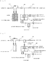
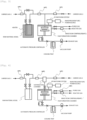
- the ALD apparatus include an apparatus capable of performing bubbling supply of a precursor as illustrated in FIG. 1 and FIG. 3 and an apparatus including a vaporization chamber as illustrated in FIG. 2 and FIG. 4 .
- Another specific example thereof is an apparatus capable of subjecting the reactive gas to plasma treatment as illustrated in FIG. 3 and FIG. 4 .
- the apparatus is not limited to such single-substrate type apparatus each including a film formation chamber (hereinafter referred to as "deposition reaction portion") as illustrated in FIG. 1 to FIG. 4 , and an apparatus capable of simultaneously processing a large number of substrates through use of a batch furnace may also be used. Those apparatus may also be used as CVD apparatus.
- a thin-film produced through use of the thin-film forming raw material of the present invention may be formed as desired kinds of thin-films, such as thin-films of a metal, oxide ceramics, nitride ceramics, and glass, by appropriately selecting the other precursor, the reactive gas, and the production conditions. It has been known that the thin-films exhibit electrical characteristics, optical characteristics, and the like, and the thin-films have been applied to various usages. Examples thereof include a metal thin-film, a metal oxide thin-film, a metal nitride thin-film, an alloy thin film, and a metal-containing composite oxide thin-film.
- Those thin-films have been widely used in the production of, for example, an electrode material for a memory element typified by a DRAM element, a resistance film, a diamagnetic film used for the recording layer of a hard disk, and a catalyst material for a polymer electrolyte fuel cell.
- amidinate compounds and dimer compounds thereof are described in Examples 1 to 3 below.
- the solvent was removed from the resultant filtrate, and the residue was distilled at a bath temperature of 125°C, a pressure of 93 Pa, and a column top temperature of 90°C to provide Compound No. 19 that was a dark blue solid in a yield of 12.6 g and a percent yield of 61%.
- the solvent was removed from the resultant filtrate, and the residue was distilled at a bath temperature of 120°C, a pressure of 110 Pa, and a column top temperature of 100°C to provide Compound No. 20 that was a dark blue liquid in a yield of 28.6 g and a percent yield of 60%.
- the weight of a test compound was measured with a TG-DTA under normal pressure at an Ar flow rate of 100 mL/min and a temperature increase rate of 10°C/min in the scanning temperature range of from 30°C to 600°C, and the temperature (°C) at which the weight of the test compound reduced by 50 mass% was evaluated as a "temperature (°C) at the time of a 50 mass% loss in normal pressure TG-DTA.”
- the results are shown in Table 1.
- the weight of a test compound was measured with a TG-DTA at 10 Torr, an Ar flow rate of 50 mL/min, and a temperature increase rate of 10°C/min in the scanning temperature range of from 30°C to 600°C, and the temperature (°C) at which the weight of the test compound reduced by 50 mass% was evaluated as a "temperature (°C) at the time of a 50 mass% loss in reduced pressure TG-DTA.”
- the results are shown in Table 1.
- Compounds No. 19 and No. 20 were compounds each having a temperature at the time of a 50 mass% loss in normal pressure TG-DTA and a temperature at the time of a 50 mass% loss in reduced pressure TG-DTA lower than those of Comparative Compound 1 by 10°C or more each.
- Compound No. 68 was a compound having a temperature at the time of a 50 mass% loss in normal pressure TG-DTA lower than that of Comparative Compound 2 by 30°C and having a temperature at the time of a 50 mass% loss in reduced pressure TG-DTA lower than that of Comparative Compound 2 by 20°C.
- the amidinate compound and the dimer compound thereof of the present invention were compounds having vapor pressures larger than those of an amidinate compound and a dimer compound thereof that had heretofore been known.
- Compounds No. 19 and No. 20 were compounds each having a melting point lower than that of Comparative Compound 1 by 45°C or more.
- Compound No. 20 was a liquid at 20°C, and was hence a compound having a particularly low melting point.
- Compound No. 68 was a compound having a melting point lower than that of Comparative Compound 2 by 15°C or more.
- a metal cobalt thin-film or a tin oxide thin-film was produced on a silicon substrate by the ALD method under the following conditions through use of an ALD apparatus illustrated in FIG. 1 with each of the compounds of the present invention obtained in Examples 1 to 3 and Comparative Compounds 1 and 2, being used as a chemical vapor deposition raw material.
- a film thickness was measured by an X-ray reflectivity method
- a compound of the thin-film was identified by an X-ray diffraction method
- the content of carbon in the thin-film was measured by X-ray photoelectron spectroscopy. The results are shown in Table 2.
- the content of carbon in the metal thin-film obtained by the ALD method is 5 atm% or more in each of Comparative Examples 1 and 2, whereas the content of carbon is less than 0.1 atm% that is the detection limit in each of Examples 4 to 6.
- the thickness of the obtained thin-film is 3.5 nm or less in each of Comparative Examples 1 and 2, whereas the thickness is 6.5 nm or more in each of Examples 4 to 6.
- the metal thin-film was obtained with high productivity through use of each of the amidinate compound and the dimer compound thereof of the present invention.
Landscapes
- Chemical & Material Sciences (AREA)
- Organic Chemistry (AREA)
- General Chemical & Material Sciences (AREA)
- Chemical Kinetics & Catalysis (AREA)
- Engineering & Computer Science (AREA)
- Materials Engineering (AREA)
- Mechanical Engineering (AREA)
- Metallurgy (AREA)
- Inorganic Chemistry (AREA)
- Chemical Vapour Deposition (AREA)
- Organic Low-Molecular-Weight Compounds And Preparation Thereof (AREA)
Applications Claiming Priority (2)
| Application Number | Priority Date | Filing Date | Title |
|---|---|---|---|
| JP2020070708 | 2020-04-10 | ||
| PCT/JP2021/013898 WO2021205958A1 (ja) | 2020-04-10 | 2021-03-31 | アミジナート化合物、その二量体化合物、薄膜形成用原料及び薄膜の製造方法 |
Publications (2)
| Publication Number | Publication Date |
|---|---|
| EP4134372A1 true EP4134372A1 (de) | 2023-02-15 |
| EP4134372A4 EP4134372A4 (de) | 2024-07-17 |
Family
ID=78023767
Family Applications (1)
| Application Number | Title | Priority Date | Filing Date |
|---|---|---|---|
| EP21783689.9A Pending EP4134372A4 (de) | 2020-04-10 | 2021-03-31 | Amidinatverbindung, dimerverbindung davon, rohmaterial zur bildung eines dünnfilms und verfahren zur herstellung eines dünnfilms |
Country Status (8)
| Country | Link |
|---|---|
| US (1) | US12275748B2 (de) |
| EP (1) | EP4134372A4 (de) |
| JP (1) | JP7787806B2 (de) |
| KR (1) | KR20220167299A (de) |
| CN (1) | CN115380038A (de) |
| IL (1) | IL297232B1 (de) |
| TW (1) | TWI873328B (de) |
| WO (1) | WO2021205958A1 (de) |
Cited By (1)
| Publication number | Priority date | Publication date | Assignee | Title |
|---|---|---|---|---|
| WO2025132279A1 (en) | 2023-12-18 | 2025-06-26 | Merck Patent Gmbh | Group 13 metal compounds for ald applications |
Families Citing this family (1)
| Publication number | Priority date | Publication date | Assignee | Title |
|---|---|---|---|---|
| JP7847144B2 (ja) * | 2021-07-12 | 2026-04-16 | 株式会社Adeka | コバルト化合物、薄膜形成用原料、薄膜及び薄膜の製造方法 |
Family Cites Families (4)
| Publication number | Priority date | Publication date | Assignee | Title |
|---|---|---|---|---|
| EP2182088B1 (de) | 2002-11-15 | 2013-07-17 | President and Fellows of Harvard College | Atomlagenabscheidung (ald) mit Hilfe von Metallamidinaten |
| WO2006012052A2 (en) * | 2004-06-25 | 2006-02-02 | Arkema, Inc. | Amidinate ligand containing chemical vapor deposition precursors |
| EP2032529B1 (de) * | 2006-06-28 | 2012-10-17 | President and Fellows of Harvard College | Metall(iv)-tetraamidinatverbindungen und ihre verwendung in der aufdampfung |
| JP7075891B2 (ja) | 2016-11-08 | 2022-05-26 | 株式会社Adeka | 化合物、薄膜形成用原料及び薄膜の製造方法 |
-
2021
- 2021-03-31 CN CN202180027605.8A patent/CN115380038A/zh active Pending
- 2021-03-31 EP EP21783689.9A patent/EP4134372A4/de active Pending
- 2021-03-31 JP JP2022514432A patent/JP7787806B2/ja active Active
- 2021-03-31 KR KR1020227038495A patent/KR20220167299A/ko active Pending
- 2021-03-31 US US17/917,671 patent/US12275748B2/en active Active
- 2021-03-31 WO PCT/JP2021/013898 patent/WO2021205958A1/ja not_active Ceased
- 2021-03-31 IL IL297232A patent/IL297232B1/en unknown
- 2021-04-08 TW TW110112649A patent/TWI873328B/zh active
Cited By (1)
| Publication number | Priority date | Publication date | Assignee | Title |
|---|---|---|---|---|
| WO2025132279A1 (en) | 2023-12-18 | 2025-06-26 | Merck Patent Gmbh | Group 13 metal compounds for ald applications |
Also Published As
| Publication number | Publication date |
|---|---|
| WO2021205958A1 (ja) | 2021-10-14 |
| KR20220167299A (ko) | 2022-12-20 |
| TW202144376A (zh) | 2021-12-01 |
| US20230151041A1 (en) | 2023-05-18 |
| IL297232A (en) | 2022-12-01 |
| IL297232B1 (en) | 2026-04-01 |
| CN115380038A (zh) | 2022-11-22 |
| EP4134372A4 (de) | 2024-07-17 |
| JPWO2021205958A1 (de) | 2021-10-14 |
| TWI873328B (zh) | 2025-02-21 |
| US12275748B2 (en) | 2025-04-15 |
| JP7787806B2 (ja) | 2025-12-17 |
Similar Documents
| Publication | Publication Date | Title |
|---|---|---|
| EP3783130A1 (de) | Quellenmaterial für dünnschichtbildung für atomlagenabscheidung und verfahren zur herstellung einer dünnschicht | |
| US11555044B2 (en) | Thin-film forming raw material for use in atomic layer deposition method, thin-film forming raw material, method for producing thin-film, and compound | |
| EP3712159B1 (de) | Rutheniumverbindung, rohstoff zur bildung einer dünnschicht, verfahren zur herstellung einer dünnschicht | |
| EP3901326A1 (de) | Ausgangsmaterial zur herstellung einer dünnschicht für die atomschichtabscheidung, verfahren zur herstellung einer dünnschicht und alkoxidverbindung | |
| US12415821B2 (en) | Tin compound, thin-film forming raw material containing said compound, thin film formed from said thin-film forming raw material, method of producing said thin film using said compound as precursor, and method of producing said thin film | |
| EP4130335A1 (de) | Material zur bildung eines dünnfilms zur verwendung bei der atomlagenabscheidung und verfahren zur herstellung eines dünnfilms | |
| US12275748B2 (en) | Amidinate compound, dimer compound thereof, thin-film forming raw material, and method of producing thin film | |
| US12276022B2 (en) | Alkoxide compound, thin-film forming raw material, and method of producing thin-film | |
| US20240425975A1 (en) | Thin-film forming raw material, method of producing thin-film, thin-film, and molybdenum compound | |
| EP4067365B1 (de) | Verbindung, dünnschichtbildendes material und verfahren zum produzieren einer dünnschicht | |
| EP3951006A1 (de) | Rohmaterial zur formung einer dünnschicht, verfahren zur herstellung einer dünnschicht und scandiumverbindung | |
| US12264168B2 (en) | Ruthenium compound, thin-film forming raw material, and method of producing thin film | |
| US12486573B2 (en) | Thin-film forming raw material, thin-film and method of producing thin-film | |
| US12577660B2 (en) | Compound, thin-film forming raw material, thin-film, and method of producing thin-film | |
| US12480207B2 (en) | Tin compound, thin-film forming raw material, thin-film, method for producing thin-film, and halogen compound | |
| US12371778B2 (en) | Cobalt compound, thin-film forming raw material, thin-film, and method of producing thin-film | |
| US20230349039A1 (en) | Thin-film forming raw material used in atomic layer deposition method, and method of producing thin-film |
Legal Events
| Date | Code | Title | Description |
|---|---|---|---|
| STAA | Information on the status of an ep patent application or granted ep patent |
Free format text: STATUS: THE INTERNATIONAL PUBLICATION HAS BEEN MADE |
|
| PUAI | Public reference made under article 153(3) epc to a published international application that has entered the european phase |
Free format text: ORIGINAL CODE: 0009012 |
|
| STAA | Information on the status of an ep patent application or granted ep patent |
Free format text: STATUS: REQUEST FOR EXAMINATION WAS MADE |
|
| 17P | Request for examination filed |
Effective date: 20221103 |
|
| AK | Designated contracting states |
Kind code of ref document: A1 Designated state(s): AL AT BE BG CH CY CZ DE DK EE ES FI FR GB GR HR HU IE IS IT LI LT LU LV MC MK MT NL NO PL PT RO RS SE SI SK SM TR |
|
| DAV | Request for validation of the european patent (deleted) | ||
| DAX | Request for extension of the european patent (deleted) | ||
| REG | Reference to a national code |
Ref country code: DE Ref legal event code: R079 Free format text: PREVIOUS MAIN CLASS: C07F0015060000 Ipc: C07C0257140000 |
|
| A4 | Supplementary search report drawn up and despatched |
Effective date: 20240619 |
|
| RIC1 | Information provided on ipc code assigned before grant |
Ipc: C23C 16/455 20060101ALI20240613BHEP Ipc: C23C 16/18 20060101ALI20240613BHEP Ipc: C07F 7/22 20060101ALI20240613BHEP Ipc: C07F 7/10 20060101ALI20240613BHEP Ipc: C07F 5/00 20060101ALI20240613BHEP Ipc: C07C 257/14 20060101AFI20240613BHEP |