EP4134743A1 - Verfahren zur herstellung einer mikro-nano-struktur - Google Patents
Verfahren zur herstellung einer mikro-nano-struktur Download PDFInfo
- Publication number
- EP4134743A1 EP4134743A1 EP21795876.8A EP21795876A EP4134743A1 EP 4134743 A1 EP4134743 A1 EP 4134743A1 EP 21795876 A EP21795876 A EP 21795876A EP 4134743 A1 EP4134743 A1 EP 4134743A1
- Authority
- EP
- European Patent Office
- Prior art keywords
- fluid polymer
- micro
- light
- mask
- substrate
- Prior art date
- Legal status (The legal status is an assumption and is not a legal conclusion. Google has not performed a legal analysis and makes no representation as to the accuracy of the status listed.)
- Pending
Links
Images




Classifications
-
- G—PHYSICS
- G03—PHOTOGRAPHY; CINEMATOGRAPHY; ANALOGOUS TECHNIQUES USING WAVES OTHER THAN OPTICAL WAVES; ELECTROGRAPHY; HOLOGRAPHY
- G03F—PHOTOMECHANICAL PRODUCTION OF TEXTURED OR PATTERNED SURFACES, e.g. FOR PRINTING, FOR PROCESSING OF SEMICONDUCTOR DEVICES; MATERIALS THEREFOR; ORIGINALS THEREFOR; APPARATUS SPECIALLY ADAPTED THEREFOR
- G03F7/00—Photomechanical, e.g. photolithographic, production of textured or patterned surfaces, e.g. printing surfaces; Materials therefor, e.g. comprising photoresists; Apparatus specially adapted therefor
- G03F7/0002—Lithographic processes using patterning methods other than those involving the exposure to radiation, e.g. by stamping
-
- G—PHYSICS
- G03—PHOTOGRAPHY; CINEMATOGRAPHY; ANALOGOUS TECHNIQUES USING WAVES OTHER THAN OPTICAL WAVES; ELECTROGRAPHY; HOLOGRAPHY
- G03F—PHOTOMECHANICAL PRODUCTION OF TEXTURED OR PATTERNED SURFACES, e.g. FOR PRINTING, FOR PROCESSING OF SEMICONDUCTOR DEVICES; MATERIALS THEREFOR; ORIGINALS THEREFOR; APPARATUS SPECIALLY ADAPTED THEREFOR
- G03F7/00—Photomechanical, e.g. photolithographic, production of textured or patterned surfaces, e.g. printing surfaces; Materials therefor, e.g. comprising photoresists; Apparatus specially adapted therefor
- G03F7/70—Microphotolithographic exposure; Apparatus therefor
- G03F7/70425—Imaging strategies, e.g. for increasing throughput or resolution, printing product fields larger than the image field or compensating lithography- or non-lithography errors, e.g. proximity correction, mix-and-match, stitching or double patterning
- G03F7/70433—Layout for increasing efficiency or for compensating imaging errors, e.g. layout of exposure fields for reducing focus errors; Use of mask features for increasing efficiency or for compensating imaging errors
-
- G—PHYSICS
- G03—PHOTOGRAPHY; CINEMATOGRAPHY; ANALOGOUS TECHNIQUES USING WAVES OTHER THAN OPTICAL WAVES; ELECTROGRAPHY; HOLOGRAPHY
- G03F—PHOTOMECHANICAL PRODUCTION OF TEXTURED OR PATTERNED SURFACES, e.g. FOR PRINTING, FOR PROCESSING OF SEMICONDUCTOR DEVICES; MATERIALS THEREFOR; ORIGINALS THEREFOR; APPARATUS SPECIALLY ADAPTED THEREFOR
- G03F7/00—Photomechanical, e.g. photolithographic, production of textured or patterned surfaces, e.g. printing surfaces; Materials therefor, e.g. comprising photoresists; Apparatus specially adapted therefor
- G03F7/16—Coating processes; Apparatus therefor
- G03F7/162—Coating on a rotating support, e.g. using a whirler or a spinner
-
- G—PHYSICS
- G03—PHOTOGRAPHY; CINEMATOGRAPHY; ANALOGOUS TECHNIQUES USING WAVES OTHER THAN OPTICAL WAVES; ELECTROGRAPHY; HOLOGRAPHY
- G03F—PHOTOMECHANICAL PRODUCTION OF TEXTURED OR PATTERNED SURFACES, e.g. FOR PRINTING, FOR PROCESSING OF SEMICONDUCTOR DEVICES; MATERIALS THEREFOR; ORIGINALS THEREFOR; APPARATUS SPECIALLY ADAPTED THEREFOR
- G03F7/00—Photomechanical, e.g. photolithographic, production of textured or patterned surfaces, e.g. printing surfaces; Materials therefor, e.g. comprising photoresists; Apparatus specially adapted therefor
- G03F7/16—Coating processes; Apparatus therefor
- G03F7/168—Finishing the coated layer, e.g. drying, baking, soaking
-
- G—PHYSICS
- G03—PHOTOGRAPHY; CINEMATOGRAPHY; ANALOGOUS TECHNIQUES USING WAVES OTHER THAN OPTICAL WAVES; ELECTROGRAPHY; HOLOGRAPHY
- G03F—PHOTOMECHANICAL PRODUCTION OF TEXTURED OR PATTERNED SURFACES, e.g. FOR PRINTING, FOR PROCESSING OF SEMICONDUCTOR DEVICES; MATERIALS THEREFOR; ORIGINALS THEREFOR; APPARATUS SPECIALLY ADAPTED THEREFOR
- G03F7/00—Photomechanical, e.g. photolithographic, production of textured or patterned surfaces, e.g. printing surfaces; Materials therefor, e.g. comprising photoresists; Apparatus specially adapted therefor
- G03F7/70—Microphotolithographic exposure; Apparatus therefor
- G03F7/70216—Mask projection systems
- G03F7/7035—Proximity or contact printers
Definitions
- the present disclosure relates to a field of micro-nano fabricating technology, and in particular to a method of fabricating a micro-nano structure.
- an artificial structure with a micro-nano feature scale may greatly enhance performances of a micro-nano photonic device, a micro-nano electronic device, a micro-nano electromechanical system, a micro-nano energy source and a display device.
- a requirement for low-cost, high-resolution, high-yield, and large-scale novel nano fabricating techniques/methods is extremely urgent.
- Traditional micro-nano fabricating techniques are generally divided into three categories: direct writing, lithography, and imprinting.
- the direct-writing micro-nano fabricating technique has a high resolution, it has a low fabricating efficiency and thus is not applicable for large-scale mass production.
- the photolithography micro-nano fabricating technique has great technical advantages in terms of efficiency, material, and process compatibility, etc.
- Rayleigh criterion theory it is necessary to use an objective lens with a shorter exposure wavelength and a higher numerical aperture in order to improve an exposure resolution, which means an accompanying rising cost.
- the imprinting micro-nano fabricating technique is a low-cost fabricating technique developed in recent years.
- the present disclosure provides a method of fabricating a micro-nano structure for at least partially solving the technical problems such as low processing efficiency, high fabricating cost, and massive pattern defects of traditional micro-nano fabricating techniques.
- a method of fabricating a micro-nano structure including: forming a reflective layer and a fluid polymer layer sequentially on a surface of a substrate; pressurizing the substrate and a mask having a micro-nano pattern to attach to each other, squeezing the fluid polymer layer into a light-transmission area of the mask, and curing the fluid polymer layer; and exposing, wherein a fluid polymer in the light-transmission area is configured to sense light under a combined effect of a transmitted light and a light reflected by the reflective layer, such that a micro-nano structure is obtained.
- the pressurizing the substrate and a mask having a micro-nano pattern to attach to each other includes: pressurizing the substrate and the mask having the micro-nano pattern to attach to each other through a precise pressure transfer, such that the fluid polymer layer is uniformly pressurized into the light-transmission area of the mask.
- a method of the precise pressure transfer includes piston-type mechanical transfer, piezoelectric actuator transfer, gas film transfer, and gas pressure transfer.
- the method further includes: leveling and contacting the substrate with the mask having the micro-nano pattern.
- the curing the fluid polymer in the light-transmission area further includes: placing the substrate in a developing solution for development, and removing the fluid polymer not sensing light and not cured, so as to obtain the micro-nano structure.
- a micro-nano pattern of the mask further includes an anti-adhesion layer, and a material of the anti-adhesion layer includes diamond-like carbon thin film or fluorine-doped silane.
- the fluid polymer layer is a high-resolution fluid polymer material, including fluorine-doped silicon-based copolymer or derivative, vinyl ether-based copolymer, acrylic-based copolymer, calixarene-based molecular glass, acetal polymer with high acid hydrolysis activity, or poly p-hydroxystyrene-based copolymer.
- a method of forming the reflective layer on the surface of the substrate includes molecular beam epitaxy in combination with low temperature annealing, co-sputtering, and high temperature sputtering.
- forming the fluid polymer layer on the surface of the substrate includes spin-coating the fluid polymer on a surface of the reflective layer to form the fluid polymer layer.
- the reflective layer includes a low-loss silver reflective layer and a low-loss aluminum reflective layer.
- a method of fabricating a micro-nano optical printing based on reflective light field enhancement including the following steps: step 1, depositing a low-loss reflective layer on a surface of a substrate; step 2, spin-coating a high-resolution fluid polymer material on a surface of the reflective layer; step 3, preparing an anti-adhesion layer on a surface of a micro-nano mask; step 4, leveling and contacting, by a mechanical device, the substrate with the high-resolution fluid polymer material spin-coated on the surface of the reflective layer with a surface of a micro-nano mask pattern; step 5, squeezing, by using a method of precise pressure transfer, a shallow surface layer of the high-resolution fluid polymer material into a light-transmission area of the mask pattern; step 6, exposing, wherein a light field local passing through the mask pattern is located in the light-transmission area under an effect of the reflective layer, such that a local part of the fluid polymer material between
- a method of fabricating the low-loss reflective layer in step 1 is molecular beam epitaxy in combination with low temperature annealing, co-sputtering, or high temperature sputtering.
- the high-resolution fluid polymer material in step 2 is a fluorine-doped silicon-based copolymer or derivative, a vinyl ether-based copolymer, an acrylic-based copolymer, calixarene-based molecular glass, an acetal polymer with high acid hydrolysis activity, or a poly p-hydroxystyrene-based copolymer.
- the anti-adhesion layer in step 3 is a diamond-like carbon thin film or a fluorine-doped silane.
- step 5 is piston-type mechanical transfer, piezoelectric actuator transfer, gas film transfer, or gas pressure transfer.
- a method of pressure transfer in step 5 is piston-type mechanical transfer, piezoelectric actuator transfer, gas film transfer, or gas pressure transfer.
- a method of fabricating a micro-nano structure provided by the present disclosure improves the processing resolution by reducing the transmission loss of evanescent waves through reflective light field enhancement, thereby solving the problem of limited diffraction.
- Shallow pressurizing in combination with exposure is used, and the depth of the pattern is mainly determined by a depth of exposure, thereby reducing the difficulty and cost of mask processing.
- the pattern squeezed into the mask is shallow, and the depth of the pattern is mainly increased by exposure, thereby greatly reducing pattern defects.
- Embodiments of the present disclosure provide a method of fabricating a micro-nano structure, where a reflective layer is formed on a substrate, and a method of shallow pressurizing in combination with exposure is used so as to propose a method of fabricating micro-nano optical print based on reflective light field enhancement, thereby providing a technical support for solving the aforementioned problems.
- FIG. 1 schematically shows a schematic flow chart of a method of fabricating a micro-nano structure according to an embodiment of the present disclosure.
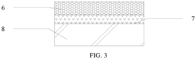
- a reflective layer 7 and a fluid polymer layer 6 are sequentially formed on a surface of a substrate 8.
- FIG 2 schematically shows a schematic diagram of fabricating a micro-nano structure according to an embodiment of the present disclosure.
- a layer of low-loss reflective layer 7 is deposited on the surface of the substrate 8; and then a high-resolution fluid polymer material is spin-coated on a surface of the reflective layer 7.
- the reflective layer 7 may reflect transmitted ultraviolet light to make the fluid polymer 6 in a transmission area sense light, so as to reduce a transmission loss of evanescent waves. In this way, a processing resolution is improved, it is not necessary to shorten an exposure wavelength and increase a numerical aperture of an objective lens, thereby reducing a production cost.
- the fluid polymer material of the fluid polymer layer 6 has a high resolution and is applicable for fabricating a micro-nano structure.
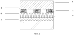
- the substrate 8 and a mask 2 having a micro-nano pattern are pressurized to attach to each other, so that the fluid polymer layer 6 is squeezed into a light-transmission area 5 of the mask, and the fluid polymer layer 6 is cured.
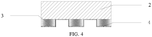
- FIG. 4 is a schematic diagram of a sectional structure of the mask 2 having the micro-nano pattern.
- an imprinting adhesive is squeezed into a stamper and then a pattern is formed by thermal curing or ultraviolet curing, a depth of the pattern is determined by the stamper, and thus the stamper is difficult to fabricate and a cost is relatively high.
- a method of shallow pressurizing in combination with exposure is used, and the depth of the pattern is mainly determined by an exposure depth, thereby reducing a difficulty and a cost of mask processing.
- a pattern structure inevitably fails to be detached from the stamper due to a force during a demolding process, resulting in pattern defects.
- the pattern squeezed into the mask is shallow, and the depth of the pattern is mainly increased by exposure, thereby greatly reducing the pattern defects.
- squeezing the fluid polymer layer 6 into the light-transmission area 5 of the mask by pressurizing does not mean that the fluid polymer layer 6 completely fills the entire light-transmission area 5, but partially fills the light-transmission area 5 of the mask.
- FIG. 6 there is still a certain gap between the fluid polymer layer 6 and a base of the mask 2 after squeezing.
- a requirement for a high resolution of the stamper is reduced through shallow pressurizing, and a production cost of the stamper is reduced.
- the pattern squeezed into the mask is shallow, pattern defects caused by uneven force applied during a process of the stamper detaching from the substrate 8 are reduced.
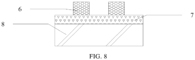
- FIG. 8 is a schematic diagram of a sectional structure of a replicated pattern obtained after development, that is, a section of an obtained micro-nano structure.
- pressurizing the substrate 8 and the mask 2 having the micro-nano pattern to attach to each other includes: pressurizing the substrate 8 and the mask 2 having the micro-nano pattern to attach to each other through precise pressure transfer, such that the fluid polymer layer 6 is uniformly pressurized into the light-transmission area 5 of the mask.
- the fluid polymer layer 6 may be uniformly pressurized into the light-transmission region 5 with a controllable depth.
- a method of precise pressure transfer includes: piston-type mechanical transfer, piezoelectric actuator transfer, gas film transfer, and gas pressure transfer.
- the piston-type mechanical transfer is precisely controlled to transfer pressure to the substrate 8 through a reciprocating motion of a piston unit, so as to pressurize the substrate 8 to attach to the mask 2.
- the piezoelectric actuator transfer is pressure transfer based on a piezoelectric effect, in which a measured pressure is transferred to a piezoelectric element by a membrane, then the piezoelectric element outputs an electrical signal having a certain relationship with the measured pressure, thereby precisely controlling the pressure applied to the substrate.
- the gas film transfer is that a certain gas pressure difference is generated when an inner pressure of a gas film is greater than an outer pressure of the gas film, such that the gas in the gas film may support a film material to apply pressure on the substrate.
- Gas pressure transfer is to increase the pressure by compressing the gas, so as to apply pressure to the substrate.
- the above methods may control a magnitude of the pressure applied to the substrate, with a uniform distribution of the applied pressure on a surface of the substrate, thereby realizing a precise control of the squeezing depth, such that the finally obtained micro-nano structure has the high resolution.
- the method further includes: the substrate 8 and the mask 2 having the micro-nano pattern are leveled and brought into contact with each other.
- the substrate 8 with the high-resolution fluid polymer material spin-coated on a surface of the reflective layer 7 and a surface of the micro-nano mask pattern are required to be leveled and brought into contact with each other by a mechanical device, so as to avoid pattern defects caused by non-uniform depth of the pressed fluid polymer 6 due to the uneven contact surface.
- curing the fluid polymer in the light-transmission area further includes: the substrate 8 is placed in a developing solution for development, and the fluid polymer not sensing light and not cured is removed so as to obtain the micro-nano structure.
- FIG. 7 is a schematic diagram of a sectional structure of demolding after the exposure is completed.
- the substrate is placed into the developing solution for development after demolding, and the polymer material not sensing light and not cured is removed.
- the polymer material not sensing light and not cured is mainly located between the mask pattern area 3 and the reflective layer 7. That is, the area with the mask pattern is replicated to the substrate 8, and the remaining pattern is the light-transmission area of the mask 2, such that the replicated pattern is finally obtained on the substrate, thereby realizing a transfer of the pattern from the mask 2.
- FIG. 8 is a schematic diagram of a sectional structure of a replicated pattern obtained after development.
- the micro-nano pattern 3 of the mask 2 also includes an anti-adhesion layer 4, and a material of the anti-adhesion layer 4 includes a diamond-like carbon thin film and a fluorine-doped silane.
- FIG. 4 is a schematic diagram of a sectional structure after an anti-adhesion layer 4 is fabricated on a surface of a micro-nano mask.
- the diamond-like carbon thin film combines excellent properties of diamond and graphite.
- the diamond-like carbon thin film is used as the anti-adhesion layer due to its high hardness and good optical transparency, thus the diamond-like carbon thin film is difficult to adhere to the fluid polymer layer 6 and does not affect a subsequent exposure process.
- fluorine-containing polysiloxane has characteristics of low surface energy, solvent resistance, flexibility, high and low temperature resistance, and possesses good hydrophobicity, oleophobicity, and stain resistance properties, thus anti-adhesion properties of the mask 2 may be improved.
- the fluid polymer layer 6 is a high-resolution fluid polymer material, including a fluorine-doped silicon-based copolymer or derivative, a vinyl ether-based copolymer, an acrylic-based copolymer, calixarene-based molecular glass, an acetal polymer with high acid hydrolysis activity, and a poly p-hydroxystyrene-based copolymer.
- the requirements include a resolution being less than 100 nanometers, a viscosity being less than 5 ⁇ 10 -3 Pa ⁇ s, a molecular weight being less than 40, a contrast ratio being greater than 4, etc.
- the fluid polymer layer 6 of the present disclosure may be made of materials such as a fluorine-doped silicon-based copolymer or derivative, a vinyl ether-based copolymer, an acrylic-based copolymer, calixarene-based molecular glass, an acetal polymer with high acid hydrolysis activity, and a poly p-hydroxystyrene-based copolymer.
- the method of forming the reflective layer 7 on the surface of the substrate 8 includes: molecular beam epitaxy combined with low temperature annealing, a co-sputtering method, and a high temperature sputtering method.
- the reflective layer 7 is usually made of a metal or metal alloy, which is mainly deposited by means of vacuum coating and sputtering.
- the molecular beam epitaxy may be used to prepare single crystal thin films as thin as dozens of atomic layers, a growth quality is high, so that a high-quality reflective layer 7 is easily obtained.
- the sputtering has advantages of easy control, large coating area, strong adhesion, etc., so that the high-quality reflective layer 7 is also easily obtained.
- the forming the fluid polymer layer 6 on the surface of the substrate 8 includes: the fluid polymer is spin-coated on the surface of the reflective layer 7 to form the fluid polymer layer.
- a main advantage of spin coating is that it is easy to obtain a dense coating with a relatively uniform coating thickness.
- the use of spin-coating to form the fluid polymer layer 6 is mainly to obtain a coating with a uniform thickness, so as to ensure that a fluid to be squeezed has a consistent depth subsequently.
- the reflective layer 7 includes a low-loss silver reflective layer and a low-loss aluminum reflective layer.
- Materials used for the reflective layer here include silver, silver alloys (such as an Ag-Pd alloy), aluminum, and aluminum alloys (such as an Al-Ti alloy). These materials all exhibit high reflectivity, which may minimize the transmission loss of the evanescent waves, and thus the processing resolution may be improved.
- An optical printing pattern with a line width resolution of 200 nm and a depth of 300 nm is fabricated.
- a specific fabricating process is as follows.
- An optical printing pattern with a line width resolution of 30 nm and a depth of 50 nm is fabricated.
- a specific fabricating process is as follows.
- the method of the present disclosure Compared with the traditional direct-writing micro-nano fabricating techniques, although the method of the present disclosure also needs to fabricate the mask by direct-writing, micro-nano structures may be replicated in batches at low cost by using the mask, and the processing efficiency is much higher than that of the traditional direct-writing micro-nano fabricating techniques.
- the method of the present disclosure solves the problem of limited diffraction, and improves the processing resolution by reducing the transmission loss of evanescent waves through reflective light field enhancement, there is no need to shorten the exposure wavelength and improve the numerical aperture of the objective lens.
- the present method uses the shallow pressurizing in combination with the exposure, and the depth of the pattern is mainly determined by the depth of exposure, thereby reducing the difficulty and cost of mask processing.
- the pattern structure since it is necessary to ensure a certain aspect ratio of the imprint pattern, the pattern structure inevitably fails to be detached from the stamper due to the force during the demolding process, resulting in the pattern defects.
- the pattern squeezed into the mask is shallow, and the depth of the pattern is mainly increased by exposure, thereby greatly reducing the pattern defects.
Landscapes
- Physics & Mathematics (AREA)
- General Physics & Mathematics (AREA)
- Shaping Of Tube Ends By Bending Or Straightening (AREA)
- Exposure Of Semiconductors, Excluding Electron Or Ion Beam Exposure (AREA)
- Optical Filters (AREA)
- Exposure And Positioning Against Photoresist Photosensitive Materials (AREA)
- Optical Elements Other Than Lenses (AREA)
Applications Claiming Priority (2)
| Application Number | Priority Date | Filing Date | Title |
|---|---|---|---|
| CN202010354559.XA CN111522206B (zh) | 2020-04-29 | 2020-04-29 | 一种基于反射式光场增强的微纳光印制造方法 |
| PCT/CN2021/090554 WO2021219005A1 (zh) | 2020-04-29 | 2021-04-28 | 一种微纳结构的制备方法 |
Publications (2)
| Publication Number | Publication Date |
|---|---|
| EP4134743A1 true EP4134743A1 (de) | 2023-02-15 |
| EP4134743A4 EP4134743A4 (de) | 2023-09-27 |
Family
ID=71903753
Family Applications (1)
| Application Number | Title | Priority Date | Filing Date |
|---|---|---|---|
| EP21795876.8A Pending EP4134743A4 (de) | 2020-04-29 | 2021-04-28 | Verfahren zur herstellung einer mikro-nano-struktur |
Country Status (5)
| Country | Link |
|---|---|
| US (1) | US11675273B2 (de) |
| EP (1) | EP4134743A4 (de) |
| JP (1) | JP7333676B2 (de) |
| CN (1) | CN111522206B (de) |
| WO (1) | WO2021219005A1 (de) |
Families Citing this family (1)
| Publication number | Priority date | Publication date | Assignee | Title |
|---|---|---|---|---|
| CN111522206B (zh) * | 2020-04-29 | 2021-09-21 | 中国科学院光电技术研究所 | 一种基于反射式光场增强的微纳光印制造方法 |
Family Cites Families (23)
| Publication number | Priority date | Publication date | Assignee | Title |
|---|---|---|---|---|
| US8728380B2 (en) * | 1995-11-15 | 2014-05-20 | Regents Of The University Of Minnesota | Lithographic method for forming a pattern |
| US6653030B2 (en) | 2002-01-23 | 2003-11-25 | Hewlett-Packard Development Company, L.P. | Optical-mechanical feature fabrication during manufacture of semiconductors and other micro-devices and nano-devices that include micron and sub-micron features |
| JP4183245B2 (ja) * | 2003-05-12 | 2008-11-19 | キヤノン株式会社 | アライメント方法、該アライメント方法を用いた露光方法 |
| US7654816B2 (en) | 2004-10-07 | 2010-02-02 | Hewlett-Packard Development Company, L.P. | Lithographic mask alignment |
| KR101352360B1 (ko) | 2005-04-27 | 2014-01-15 | 오브듀캇 아베 | 물체에 패턴을 전사하기 위한 수단 |
| JP5271486B2 (ja) * | 2006-08-16 | 2013-08-21 | 株式会社ブリヂストン | 離型剤、これを用いた凹凸パターンの形成方法及び光情報記録媒体の製造方法、並びに光情報記録媒体 |
| KR100843342B1 (ko) * | 2007-02-12 | 2008-07-03 | 삼성전자주식회사 | Uv 나노 임프린트 리소그래피 수행 공정 및 장치 |
| JP5570688B2 (ja) * | 2007-06-28 | 2014-08-13 | ピーエスフォー ルクスコ エスエイアールエル | 微細レジストパターン形成方法及びナノインプリントモールド構造 |
| CN101131537B (zh) * | 2007-09-13 | 2011-04-20 | 苏州苏大维格数码光学有限公司 | 一种精密数字化微纳米压印的方法 |
| CN102211441B (zh) * | 2010-02-23 | 2014-02-12 | 乐金显示有限公司 | 辊模、制造辊模的方法及采用辊模形成薄膜图案的方法 |
| JP2013069921A (ja) | 2011-09-22 | 2013-04-18 | Toshiba Corp | インプリント方法 |
| TWI570771B (zh) * | 2011-12-19 | 2017-02-11 | 分子壓模公司 | 使用步進及重複工具之用於壓印微影術之無接縫大區域主模板之製造技術 |
| JP5774536B2 (ja) * | 2012-03-30 | 2015-09-09 | 株式会社東芝 | 近接場露光用マスクおよびパターン形成方法 |
| CN103488046B (zh) | 2013-09-26 | 2019-10-22 | 上海集成电路研发中心有限公司 | 一种纳米压印光刻装置及其方法 |
| CN103631089B (zh) * | 2013-12-08 | 2016-08-17 | 中国科学院光电技术研究所 | 一种紫外光固化纳米压印聚合物模板的制备方法 |
| JP2015169803A (ja) | 2014-03-07 | 2015-09-28 | 株式会社東芝 | マスク及びパターン形成方法 |
| JP6750188B2 (ja) * | 2014-12-25 | 2020-09-02 | デクセリアルズ株式会社 | マスターフィルム付きナノ構造フィルム及びその製造方法 |
| US10468249B2 (en) | 2015-09-28 | 2019-11-05 | Taiwan Semiconductor Manufacturing Company, Ltd. | Patterning process of a semiconductor structure with a middle layer |
| US10497564B1 (en) * | 2017-07-17 | 2019-12-03 | Northrop Grumman Systems Corporation | Nano-imprinting using high-pressure crystal phase transformations |
| CN107561857A (zh) * | 2017-09-20 | 2018-01-09 | 南方科技大学 | 一种基于纳米压印制备光学超构表面的方法 |
| JP7023744B2 (ja) * | 2018-02-28 | 2022-02-22 | キヤノン株式会社 | インプリント方法及び製造方法 |
| CN109283788B (zh) * | 2018-10-11 | 2022-05-20 | 中国石油大学(华东) | 一种用于旋转式近场光刻的纳米图形加工系统及方法 |
| CN111522206B (zh) | 2020-04-29 | 2021-09-21 | 中国科学院光电技术研究所 | 一种基于反射式光场增强的微纳光印制造方法 |
-
2020
- 2020-04-29 CN CN202010354559.XA patent/CN111522206B/zh active Active
-
2021
- 2021-04-28 EP EP21795876.8A patent/EP4134743A4/de active Pending
- 2021-04-28 WO PCT/CN2021/090554 patent/WO2021219005A1/zh not_active Ceased
- 2021-04-28 JP JP2022551796A patent/JP7333676B2/ja active Active
- 2021-04-28 US US17/997,102 patent/US11675273B2/en active Active
Also Published As
| Publication number | Publication date |
|---|---|
| WO2021219005A1 (zh) | 2021-11-04 |
| CN111522206B (zh) | 2021-09-21 |
| JP2023522560A (ja) | 2023-05-31 |
| JP7333676B2 (ja) | 2023-08-25 |
| EP4134743A4 (de) | 2023-09-27 |
| CN111522206A (zh) | 2020-08-11 |
| US20230132100A1 (en) | 2023-04-27 |
| US11675273B2 (en) | 2023-06-13 |
Similar Documents
| Publication | Publication Date | Title |
|---|---|---|
| Chang et al. | A roller embossing process for rapid fabrication of microlens arrays on glass substrates | |
| JP7355918B2 (ja) | ニアアイディスプレイの回折格子導波路の製造方法 | |
| Li et al. | Hybrid nanoimprint− soft lithography with sub-15 nm resolution | |
| CN100585491C (zh) | 大面积周期阵列三维微结构制备方法 | |
| CN101446762B (zh) | 非接触式模板约束下的电场诱导微复型方法 | |
| TW200848956A (en) | Devices and methods for pattern generation by ink lithography | |
| WO2019056586A1 (zh) | 一种制备光学超构表面的方法 | |
| CN101477304A (zh) | 在复杂形状表面复制高分辨率纳米结构的压印方法及其应用 | |
| CN105487151A (zh) | 一种基于纳米压印的图形转移制备光栅的方法 | |
| CN101051184A (zh) | 大面积微纳结构软压印方法 | |
| Peng et al. | Continuous roller nanoimprinting: next generation lithography | |
| CN103328175A (zh) | 光排列一体式大面积金属印模的制造方法及利用其的高分子光元件的制造方法 | |
| CN109634055A (zh) | 一种低表面能镍纳米压印模板的制备方法 | |
| US11675273B2 (en) | Method of fabricating micro-nano structure | |
| WO2021164733A1 (zh) | 一种转移纳米结构的方法及其应用 | |
| CN101165591B (zh) | 软平板印刷技术制作二维聚合物光子晶体的方法 | |
| Gu et al. | Stretching-tunable metal gratings fabricated on an elastomeric substrate using a water-soluble sacrificial layer | |
| Rosenberg et al. | Direct resistless soft nanopatterning of freeform surfaces | |
| KR100934239B1 (ko) | 임프린트용 대면적 스탬프 제작방법 | |
| KR101542142B1 (ko) | 나노리소그래피용 마이크로팁 어레이, 이의 제조방법 및 이를 이용한 나노리소그래피 방법 | |
| KR20040033088A (ko) | 미세형상 구조물의 연속 성형방법 및 그 미세형상의성형을 위한 스탬퍼 제조방법 그리고 그 스탬퍼 | |
| Wen et al. | Innovative rapid replication of microlens arrays using electromagnetic force-assisted UV imprinting | |
| KR100731737B1 (ko) | 섀도우 마스크 기능을 갖는 자외선 경화 수지 몰딩용 복합몰드 및 그 제조 방법과 이를 이용한 패턴 형성 방법 | |
| Karkkainen et al. | Fabrication of micro-optical structures by applying negative tone hybrid glass materials and greyscale lithography | |
| US7488571B2 (en) | Method for manufacturing light guide plate |
Legal Events
| Date | Code | Title | Description |
|---|---|---|---|
| STAA | Information on the status of an ep patent application or granted ep patent |
Free format text: STATUS: THE INTERNATIONAL PUBLICATION HAS BEEN MADE |
|
| PUAI | Public reference made under article 153(3) epc to a published international application that has entered the european phase |
Free format text: ORIGINAL CODE: 0009012 |
|
| STAA | Information on the status of an ep patent application or granted ep patent |
Free format text: STATUS: REQUEST FOR EXAMINATION WAS MADE |
|
| 17P | Request for examination filed |
Effective date: 20221111 |
|
| AK | Designated contracting states |
Kind code of ref document: A1 Designated state(s): AL AT BE BG CH CY CZ DE DK EE ES FI FR GB GR HR HU IE IS IT LI LT LU LV MC MK MT NL NO PL PT RO RS SE SI SK SM TR |
|
| DAV | Request for validation of the european patent (deleted) | ||
| DAX | Request for extension of the european patent (deleted) | ||
| A4 | Supplementary search report drawn up and despatched |
Effective date: 20230824 |
|
| RIC1 | Information provided on ipc code assigned before grant |
Ipc: G03F 7/20 20060101ALI20230818BHEP Ipc: G03F 7/00 20060101AFI20230818BHEP |
|
| STAA | Information on the status of an ep patent application or granted ep patent |
Free format text: STATUS: EXAMINATION IS IN PROGRESS |
|
| 17Q | First examination report despatched |
Effective date: 20250317 |
|
| GRAP | Despatch of communication of intention to grant a patent |
Free format text: ORIGINAL CODE: EPIDOSNIGR1 |
|
| STAA | Information on the status of an ep patent application or granted ep patent |
Free format text: STATUS: GRANT OF PATENT IS INTENDED |
|
| INTG | Intention to grant announced |
Effective date: 20260112 |
|
| GRAS | Grant fee paid |
Free format text: ORIGINAL CODE: EPIDOSNIGR3 |
|
| GRAA | (expected) grant |
Free format text: ORIGINAL CODE: 0009210 |
|
| STAA | Information on the status of an ep patent application or granted ep patent |
Free format text: STATUS: THE PATENT HAS BEEN GRANTED |