EP4137622A1 - Verfahren zur herstellung eines halbleitersubstrats, halbleitersubstrat und verfahren zur verhinderung des auftretens von rissen in einer wachstumsschicht - Google Patents
Verfahren zur herstellung eines halbleitersubstrats, halbleitersubstrat und verfahren zur verhinderung des auftretens von rissen in einer wachstumsschicht Download PDFInfo
- Publication number
- EP4137622A1 EP4137622A1 EP21788428.7A EP21788428A EP4137622A1 EP 4137622 A1 EP4137622 A1 EP 4137622A1 EP 21788428 A EP21788428 A EP 21788428A EP 4137622 A1 EP4137622 A1 EP 4137622A1
- Authority
- EP
- European Patent Office
- Prior art keywords
- underlying substrate
- growth
- growth layer
- semiconductor substrate
- substrate
- Prior art date
- Legal status (The legal status is an assumption and is not a legal conclusion. Google has not performed a legal analysis and makes no representation as to the accuracy of the status listed.)
- Pending
Links
Images


Classifications
-
- C—CHEMISTRY; METALLURGY
- C04—CEMENTS; CONCRETE; ARTIFICIAL STONE; CERAMICS; REFRACTORIES
- C04B—LIME, MAGNESIA; SLAG; CEMENTS; COMPOSITIONS THEREOF, e.g. MORTARS, CONCRETE OR LIKE BUILDING MATERIALS; ARTIFICIAL STONE; CERAMICS; REFRACTORIES; TREATMENT OF NATURAL STONE
- C04B35/00—Shaped ceramic products characterised by their composition; Ceramics compositions; Processing powders of inorganic compounds preparatory to the manufacturing of ceramic products
- C04B35/515—Shaped ceramic products characterised by their composition; Ceramics compositions; Processing powders of inorganic compounds preparatory to the manufacturing of ceramic products based on non-oxide ceramics
- C04B35/58—Shaped ceramic products characterised by their composition; Ceramics compositions; Processing powders of inorganic compounds preparatory to the manufacturing of ceramic products based on non-oxide ceramics based on borides, nitrides, i.e. nitrides, oxynitrides, carbonitrides or oxycarbonitrides or silicides
- C04B35/581—Shaped ceramic products characterised by their composition; Ceramics compositions; Processing powders of inorganic compounds preparatory to the manufacturing of ceramic products based on non-oxide ceramics based on borides, nitrides, i.e. nitrides, oxynitrides, carbonitrides or oxycarbonitrides or silicides based on aluminium nitride
-
- C—CHEMISTRY; METALLURGY
- C30—CRYSTAL GROWTH
- C30B—SINGLE-CRYSTAL GROWTH; UNIDIRECTIONAL SOLIDIFICATION OF EUTECTIC MATERIAL OR UNIDIRECTIONAL DEMIXING OF EUTECTOID MATERIAL; REFINING BY ZONE-MELTING OF MATERIAL; PRODUCTION OF A HOMOGENEOUS POLYCRYSTALLINE MATERIAL WITH DEFINED STRUCTURE; SINGLE CRYSTALS OR HOMOGENEOUS POLYCRYSTALLINE MATERIAL WITH DEFINED STRUCTURE; AFTER-TREATMENT OF SINGLE CRYSTALS OR A HOMOGENEOUS POLYCRYSTALLINE MATERIAL WITH DEFINED STRUCTURE; APPARATUS THEREFOR
- C30B23/00—Single-crystal growth by condensing evaporated or sublimed materials
- C30B23/02—Epitaxial-layer growth
- C30B23/025—Epitaxial-layer growth characterised by the substrate
-
- C—CHEMISTRY; METALLURGY
- C30—CRYSTAL GROWTH
- C30B—SINGLE-CRYSTAL GROWTH; UNIDIRECTIONAL SOLIDIFICATION OF EUTECTIC MATERIAL OR UNIDIRECTIONAL DEMIXING OF EUTECTOID MATERIAL; REFINING BY ZONE-MELTING OF MATERIAL; PRODUCTION OF A HOMOGENEOUS POLYCRYSTALLINE MATERIAL WITH DEFINED STRUCTURE; SINGLE CRYSTALS OR HOMOGENEOUS POLYCRYSTALLINE MATERIAL WITH DEFINED STRUCTURE; AFTER-TREATMENT OF SINGLE CRYSTALS OR A HOMOGENEOUS POLYCRYSTALLINE MATERIAL WITH DEFINED STRUCTURE; APPARATUS THEREFOR
- C30B23/00—Single-crystal growth by condensing evaporated or sublimed materials
- C30B23/02—Epitaxial-layer growth
- C30B23/06—Heating of the deposition chamber, the substrate or the materials to be evaporated
- C30B23/063—Heating of the substrate
-
- C—CHEMISTRY; METALLURGY
- C30—CRYSTAL GROWTH
- C30B—SINGLE-CRYSTAL GROWTH; UNIDIRECTIONAL SOLIDIFICATION OF EUTECTIC MATERIAL OR UNIDIRECTIONAL DEMIXING OF EUTECTOID MATERIAL; REFINING BY ZONE-MELTING OF MATERIAL; PRODUCTION OF A HOMOGENEOUS POLYCRYSTALLINE MATERIAL WITH DEFINED STRUCTURE; SINGLE CRYSTALS OR HOMOGENEOUS POLYCRYSTALLINE MATERIAL WITH DEFINED STRUCTURE; AFTER-TREATMENT OF SINGLE CRYSTALS OR A HOMOGENEOUS POLYCRYSTALLINE MATERIAL WITH DEFINED STRUCTURE; APPARATUS THEREFOR
- C30B25/00—Single-crystal growth by chemical reaction of reactive gases, e.g. chemical vapour-deposition growth
- C30B25/02—Epitaxial-layer growth
- C30B25/18—Epitaxial-layer growth characterised by the substrate
- C30B25/186—Epitaxial-layer growth characterised by the substrate being specially pre-treated by, e.g. chemical or physical means
-
- C—CHEMISTRY; METALLURGY
- C30—CRYSTAL GROWTH
- C30B—SINGLE-CRYSTAL GROWTH; UNIDIRECTIONAL SOLIDIFICATION OF EUTECTIC MATERIAL OR UNIDIRECTIONAL DEMIXING OF EUTECTOID MATERIAL; REFINING BY ZONE-MELTING OF MATERIAL; PRODUCTION OF A HOMOGENEOUS POLYCRYSTALLINE MATERIAL WITH DEFINED STRUCTURE; SINGLE CRYSTALS OR HOMOGENEOUS POLYCRYSTALLINE MATERIAL WITH DEFINED STRUCTURE; AFTER-TREATMENT OF SINGLE CRYSTALS OR A HOMOGENEOUS POLYCRYSTALLINE MATERIAL WITH DEFINED STRUCTURE; APPARATUS THEREFOR
- C30B29/00—Single crystals or homogeneous polycrystalline material with defined structure characterised by the material or by their shape
- C30B29/10—Inorganic compounds or compositions
- C30B29/36—Carbides
-
- C—CHEMISTRY; METALLURGY
- C30—CRYSTAL GROWTH
- C30B—SINGLE-CRYSTAL GROWTH; UNIDIRECTIONAL SOLIDIFICATION OF EUTECTIC MATERIAL OR UNIDIRECTIONAL DEMIXING OF EUTECTOID MATERIAL; REFINING BY ZONE-MELTING OF MATERIAL; PRODUCTION OF A HOMOGENEOUS POLYCRYSTALLINE MATERIAL WITH DEFINED STRUCTURE; SINGLE CRYSTALS OR HOMOGENEOUS POLYCRYSTALLINE MATERIAL WITH DEFINED STRUCTURE; AFTER-TREATMENT OF SINGLE CRYSTALS OR A HOMOGENEOUS POLYCRYSTALLINE MATERIAL WITH DEFINED STRUCTURE; APPARATUS THEREFOR
- C30B29/00—Single crystals or homogeneous polycrystalline material with defined structure characterised by the material or by their shape
- C30B29/10—Inorganic compounds or compositions
- C30B29/40—AIIIBV compounds wherein A is B, Al, Ga, In or Tl and B is N, P, As, Sb or Bi
- C30B29/403—AIII-nitrides
-
- C—CHEMISTRY; METALLURGY
- C30—CRYSTAL GROWTH
- C30B—SINGLE-CRYSTAL GROWTH; UNIDIRECTIONAL SOLIDIFICATION OF EUTECTIC MATERIAL OR UNIDIRECTIONAL DEMIXING OF EUTECTOID MATERIAL; REFINING BY ZONE-MELTING OF MATERIAL; PRODUCTION OF A HOMOGENEOUS POLYCRYSTALLINE MATERIAL WITH DEFINED STRUCTURE; SINGLE CRYSTALS OR HOMOGENEOUS POLYCRYSTALLINE MATERIAL WITH DEFINED STRUCTURE; AFTER-TREATMENT OF SINGLE CRYSTALS OR A HOMOGENEOUS POLYCRYSTALLINE MATERIAL WITH DEFINED STRUCTURE; APPARATUS THEREFOR
- C30B33/00—After-treatment of single crystals or homogeneous polycrystalline material with defined structure
- C30B33/06—Joining of crystals
-
- H—ELECTRICITY
- H10—SEMICONDUCTOR DEVICES; ELECTRIC SOLID-STATE DEVICES NOT OTHERWISE PROVIDED FOR
- H10P—GENERIC PROCESSES OR APPARATUS FOR THE MANUFACTURE OR TREATMENT OF DEVICES COVERED BY CLASS H10
- H10P14/00—Formation of materials, e.g. in the shape of layers or pillars
- H10P14/20—Formation of materials, e.g. in the shape of layers or pillars of semiconductor materials
- H10P14/22—Formation of materials, e.g. in the shape of layers or pillars of semiconductor materials using physical deposition, e.g. vacuum deposition or sputtering
-
- H—ELECTRICITY
- H10—SEMICONDUCTOR DEVICES; ELECTRIC SOLID-STATE DEVICES NOT OTHERWISE PROVIDED FOR
- H10P—GENERIC PROCESSES OR APPARATUS FOR THE MANUFACTURE OR TREATMENT OF DEVICES COVERED BY CLASS H10
- H10P14/00—Formation of materials, e.g. in the shape of layers or pillars
- H10P14/20—Formation of materials, e.g. in the shape of layers or pillars of semiconductor materials
- H10P14/29—Formation of materials, e.g. in the shape of layers or pillars of semiconductor materials characterised by the substrates
- H10P14/2901—Materials
- H10P14/2902—Materials being Group IVA materials
- H10P14/2904—Silicon carbide
-
- H—ELECTRICITY
- H10—SEMICONDUCTOR DEVICES; ELECTRIC SOLID-STATE DEVICES NOT OTHERWISE PROVIDED FOR
- H10P—GENERIC PROCESSES OR APPARATUS FOR THE MANUFACTURE OR TREATMENT OF DEVICES COVERED BY CLASS H10
- H10P14/00—Formation of materials, e.g. in the shape of layers or pillars
- H10P14/20—Formation of materials, e.g. in the shape of layers or pillars of semiconductor materials
- H10P14/29—Formation of materials, e.g. in the shape of layers or pillars of semiconductor materials characterised by the substrates
- H10P14/2924—Structures
- H10P14/2925—Surface structures
-
- H—ELECTRICITY
- H10—SEMICONDUCTOR DEVICES; ELECTRIC SOLID-STATE DEVICES NOT OTHERWISE PROVIDED FOR
- H10P—GENERIC PROCESSES OR APPARATUS FOR THE MANUFACTURE OR TREATMENT OF DEVICES COVERED BY CLASS H10
- H10P14/00—Formation of materials, e.g. in the shape of layers or pillars
- H10P14/20—Formation of materials, e.g. in the shape of layers or pillars of semiconductor materials
- H10P14/32—Formation of materials, e.g. in the shape of layers or pillars of semiconductor materials characterised by intermediate layers between substrates and deposited layers
- H10P14/3202—Materials thereof
- H10P14/3214—Materials thereof being Group IIIA-VA semiconductors
- H10P14/3216—Nitrides
-
- C—CHEMISTRY; METALLURGY
- C04—CEMENTS; CONCRETE; ARTIFICIAL STONE; CERAMICS; REFRACTORIES
- C04B—LIME, MAGNESIA; SLAG; CEMENTS; COMPOSITIONS THEREOF, e.g. MORTARS, CONCRETE OR LIKE BUILDING MATERIALS; ARTIFICIAL STONE; CERAMICS; REFRACTORIES; TREATMENT OF NATURAL STONE
- C04B2235/00—Aspects relating to ceramic starting mixtures or sintered ceramic products
- C04B2235/65—Aspects relating to heat treatments of ceramic bodies such as green ceramics or pre-sintered ceramics, e.g. burning, sintering or melting processes
- C04B2235/656—Aspects relating to heat treatments of ceramic bodies such as green ceramics or pre-sintered ceramics, e.g. burning, sintering or melting processes characterised by specific heating conditions during heat treatment
- C04B2235/6565—Cooling rate
-
- C—CHEMISTRY; METALLURGY
- C04—CEMENTS; CONCRETE; ARTIFICIAL STONE; CERAMICS; REFRACTORIES
- C04B—LIME, MAGNESIA; SLAG; CEMENTS; COMPOSITIONS THEREOF, e.g. MORTARS, CONCRETE OR LIKE BUILDING MATERIALS; ARTIFICIAL STONE; CERAMICS; REFRACTORIES; TREATMENT OF NATURAL STONE
- C04B2235/00—Aspects relating to ceramic starting mixtures or sintered ceramic products
- C04B2235/65—Aspects relating to heat treatments of ceramic bodies such as green ceramics or pre-sintered ceramics, e.g. burning, sintering or melting processes
- C04B2235/656—Aspects relating to heat treatments of ceramic bodies such as green ceramics or pre-sintered ceramics, e.g. burning, sintering or melting processes characterised by specific heating conditions during heat treatment
- C04B2235/6567—Treatment time
Definitions
- the present invention relates to a method for manufacturing a semiconductor substrate, a semiconductor substrate, and a method for suppressing occurrence of cracks in a growth layer.
- a semiconductor substrate of a desired semiconductor material is manufactured by crystal-growing a semiconductor material (a so-called heteroepitaxial growth) that is different from an underlying substrate on the underlying substrate.
- an intermediate layer (a so-called buffer layer) that absorbs stress due to a lattice constant difference or a thermal expansion coefficient difference is formed between the underlying substrate and the growth layer.
- Patent Literature 1 discloses a two-step growth method in which a low-temperature growth layer is formed prior to formation of a compound semiconductor layer in order to absorb stress and crystal defects due to the lattice constant difference and the thermal expansion coefficient difference between a Si substrate and a compound semiconductor.
- Patent Literature 2 discloses a technique of inserting an aluminum nitride (AlN) layer as the buffer layer between a silicon carbide (SiC) layer and a gallium nitride (GaN) layer.
- AlN aluminum nitride
- the occurrence of cracks in the growth layer described above can also occur when the same semiconductor material as the underlying substrate is crystal-grown (a so-called homoepitaxial growth) on the underlying substrate.
- cracks may occur due to a difference in the lattice distance between the underlying substrate and the growth layer.
- An object of the present invention is to provide a novel technique capable of suppressing the occurrence of cracks in the growth layer.
- the present invention that is intended to solve the problems described above is a method for manufacturing a semiconductor substrate, which includes: an embrittlement processing step of reducing strength of an underlying substrate; and a crystal growth step of forming the growth layer on the underlying substrate.
- the embrittlement processing step of reducing the strength of the underlying substrate the stress generated in the growth layer can be released to the underlying substrate, and the occurrence of cracks in the growth layer can be suppressed.
- the crystal growth step is a step of forming the growth layer having a shrinkage rate different from that of the underlying substrate.
- the stress generated by the difference in shrinkage rate between the underlying substrate and the growth layer is released to the underlying substrate side, so that occurrence of cracks on the growth layer side can be suppressed.
- the underlying substrate and the growth layer have different doping concentrations.
- the present invention it is possible to suppress the occurrence of cracks caused by the difference in the doping concentrations between the underlying substrate and the growth layer. In other words, in the homoepitaxial growth, the occurrence of cracks in the growth layer can be suppressed.
- the underlying substrate and the growth layer are made of different materials.
- the present invention it is possible to suppress the occurrence of cracks caused by a difference in physical properties (the lattice constant and the thermal expansion coefficient) between the semiconductor material of the underlying substrate and the semiconductor material of the growth layer.
- the occurrence of cracks in the growth layer can be suppressed.
- the embrittlement processing step includes a through hole formation step of forming through holes in the underlying substrate, and a strained layer removal step of removing a strained layer introduced in the through hole formation step.
- the through hole formation step is a step of forming the through holes by irradiating the underlying substrate with a laser.
- the strained layer removal step is a step of etching the underlying substrate by heat treatment.
- the underlying substrate is silicon carbide
- the strained layer removal step is a step of etching the underlying substrate under a silicon atmosphere.
- the crystal growth step is a step of growing via a physical vapor transport method.
- the present invention also relates to a method for suppressing the occurrence of cracks in the growth layer.
- the present invention that is intended to solve the problems described above is a method for suppressing the occurrence of cracks in the growth layer, and this method includes an embrittlement processing step of reducing the strength of the underlying substrate before forming the growth layer on the underlying substrate.
- the embrittlement processing step includes a through hole formation step of forming through holes in the underlying substrate, and a strained layer removal step of removing a strained layer introduced in the through hole formation step.
- the strained layer removal step is a step of removing the strained layer of the underlying substrate by heat treatment.
- the underlying substrate is silicon carbide
- the strained layer removal step is a step of etching the underlying substrate under a silicon atmosphere.
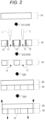
- Figs. 1 and 2 illustrate steps of a method for manufacturing a semiconductor substrate according to the embodiment of the present invention.
- the method for manufacturing the semiconductor substrate according to the embodiment may include an embrittlement processing step S10 of reducing the strength of an underlying substrate 10, a crystal growth step S20 of forming a growth layer 20 on the underlying substrate 10, and a temperature lowering step S30 of lowering the temperatures of the underlying substrate 10 and the growth layer 20 after the crystal growth step S20.
- this embodiment can be understood as a method for suppressing the occurrence of cracks in the growth layer 20 by including the embrittlement processing step S10 for reducing the strength of the underlying substrate 10 before forming the growth layer 20 on the underlying substrate 10.
- the embrittlement processing step S10 is a step of reducing the strength of the underlying substrate 10.
- the embrittlement processing step S10 is a step of processing the underlying substrate 10 in such a way to be easily deformed or broken by an external force.
- the embrittlement processing step S10 is a step of increasing the brittleness of the underlying substrate 10.
- the "strength" in the present description refers to a durability against a physical external force such as compression or tension, and includes a concept of mechanical strength.
- the embrittlement processing step S10 reduces the strength of the underlying substrate 10 by forming through holes 11 in the underlying substrate 10. In other words, by reducing the volume of the underlying substrate 10, processing is performed in such a way that the underlying substrate can be easily deformed or broken by an external force.
- the embrittlement processing step S10 includes a through hole formation step S11 of forming the through holes 11 in the underlying substrate 10, and a strained layer removal step S12 of removing a strained layer 12 introduced in the through hole formation step S11.
- the underlying substrate 10 can be naturally adopted as long as it is a material generally used in manufacturing semiconductor substrates.
- the material of the underlying substrate 10 is, for example, a known group IV material such as silicon (Si), germanium (Ge), or diamond (C).
- the material of the underlying substrate 10 is, for example, a known group IV-IV compound material such as silicon carbide (SiC).
- the material of the underlying substrate 10 is a known group II-VI compound material such as zinc oxide (ZnO), zinc sulfide (ZnS), zinc selenide (ZnSe), cadmium sulfide (CdS), or cadmium telluride (CdTe).
- the material of the underlying substrate 10 is, for example, a known group III-V compound material such as boron nitride (BN), gallium arsenide (GaAs), gallium nitride (GaN), aluminum nitride (AlN), indium nitride (InN), gallium phosphide (GaP), indium phosphide (InP), or indium antimonide (InSb).
- the material of the underlying substrate 10 is, for example, an oxide material such as aluminum oxide (Al 2 O 3 ) or gallium oxide (Ga 2 O 3 ).
- the material of the underlying substrate 10 is, for example, a metal material such as copper (Cu) or nickel (Ni). Note that the underlying substrate 10 may have a configuration in which a known additive atom to be used according to the material is appropriately added.
- a wafer or a substrate processed from a bulk crystal may be used, or a substrate having a buffer layer made of the semiconductor material described above may be separately used.
- the through hole formation step S11 is a step of reducing the strength of the underlying substrate 10 by forming the through holes 11 in the underlying substrate 10.
- the through hole formation step S11 can be naturally adopted as long as it is a method capable of forming the through holes 11 in the underlying substrate 10.
- a plasma etching such as a laser processing, a focused ion beam system (FIB), and a reactive ion etching (RIE) can be adopted as an example.
- FIB focused ion beam system
- RIE reactive ion etching
- a shape that reduces the strength of the underlying substrate 10 may be adopted for the through holes 11, and one or a plurality of through holes may be formed.
- a through hole group (pattern) in which a plurality of through holes 11 are arranged may be adopted.
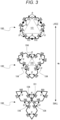
- Fig. 3 is an explanatory view for explaining a pattern 100 according to the embodiment.
- a line segment indicated by the pattern 100 is the underlying substrate 10.
- the pattern 100 preferably presents a regular hexagonal displacement shape that is three-fold symmetric.
- the "regular hexagonal displacement shape" in the description of the present description will be described in detail below with reference to Fig. 3 .
- the regular hexagonal displacement shape is a 12 polygon.
- the regular hexagonal displacement shape is constituted by 12 straight line segments having the same length.
- the pattern 100 having the regular hexagonal displacement shape includes a reference figure 101 which is regular triangle having an area 101a and including three vertices 104. Each of the three vertices 104 is included in the vertices of the pattern 100.
- the three vertices 104 may be located on a line segment constituting the pattern 100.
- the pattern 100 includes line segments 102 (corresponding to first line segments) extending from the vertices 104 and including the vertices 104, and line segments 103 (corresponding to second line segments) not extending from the vertices 104, not including the vertices 104, and adjacent to the line segments 102.
- an angle ⁇ formed by two adjacent line segments 102 in the pattern 100 is constant and is equal to an angle ⁇ formed by two adjacent line segments 103 in the pattern 100.
- the "regular hexagonal displacement shape" in the description of the present description can be understood as a 12 polygon in which the regular hexagon is displaced (deformed) while maintaining the area of the regular hexagon based on the angle ⁇ indicating a degree of unevenness.
- the angle ⁇ is preferably more than 60°, preferably 66° or more, preferably 80° or more, preferably 83° or more, preferably 120° or more, preferably 150° or more, and preferably 155° or more.
- the angle ⁇ is preferably 180° or less, preferably 155° or less, preferably 150° or less, preferably 120° or less, preferably 83° or less, preferably 80° or less, and preferably 66° or less.
- the pattern 100 may be configured to have a regular 12 polygonal displacement shape that is six-fold symmetric instead of the regular hexagonal displacement shape that is three-fold symmetric.
- the regular 12 polygonal displacement shape is a 24 polygon.
- the regular 12 polygonal displacement shape is constituted by 24 straight line segments having the same length.
- the pattern 100 having the regular 12 polygonal displacement shape includes a reference figure 101 which is regular hexagon having an area 101a and including six vertices 104. Each of the six vertices 104 is included in the vertices of the pattern 100.
- an angle ⁇ formed by two adjacent line segments 102 in the pattern 100 is constant and is equal to an angle ⁇ formed by two adjacent line segments 103 in the pattern 100.
- the "regular 12 polygonal displacement shape" in the description of the present description can be understood as a 24 polygon in which the regular 12 polygon is displaced (deformed) while maintaining the area of the regular 12 polygon based on the angle ⁇ indicating the degree of unevenness.
- the pattern 100 may have a 2n-gonal displacement shape that is a 4n-gonal shape in which a regular 2n-gonal shape is displaced (deformed) while maintaining the area of the regular 2n-gonal shape based on an angle ⁇ indicating the degree of unevenness.
- the 2n-gonal displacement shape includes a regular n-gonal shape (corresponding to the reference figure 101).
- the reference figure 101 includes n vertices.
- the pattern 100 may be configured to include a regular 2n-gonal displacement shape (the regular hexagonal displacement shape and the regular 12 polygonal displacement shape are included). Furthermore, the pattern 100 may be configured to further include at least one line segment (corresponding to a third line segment) connecting an intersection of two adjacent line segments 103 in the regular 2n-gonal displacement shape and the center of gravity of the reference figure 101, in addition to the line segment constituting the regular 2n-gonal displacement shape. Moreover, the pattern 100 may be configured to further include at least one line segment connecting an intersection of two adjacent line segments 103 in the regular 2n-gonal displacement shape and the vertices 104 constituting the reference figure 101, in addition to the line segment constituting the regular 2n-gonal displacement shape. In addition, the pattern 100 may further include at least one line segment constituting the reference figure 101 included in the regular 2n-gonal displacement shape, in addition to the line segment constituting the regular 2n-gonal displacement shape.
- the through hole formation step S11 is preferably a step of removing 50% or more of an effective area of the underlying substrate 10. Furthermore, the step of removing 60% or more of the effective area is more preferable, the step of removing 70% or more of the effective area is further preferable, and the step of removing 80% or more of the effective area is still more preferable.
- the effective area in the present description refers to the surface of the underlying substrate 10 to which the source adheres in the crystal growth step S20. In other words, it refers to a remaining region other than a region removed by the through holes 11 on the growth surface of the underlying substrate 10.
- the effective area of the underlying substrate 10 and the shape/pattern of the through holes 11 are desirably set in consideration of the lattice constant difference and the thermal expansion coefficient difference between the underlying substrate 10 and the growth layer 20, and a crystal structure and a growth method of the growth layer 20.
- the strained layer removal step S12 is a step of removing the strained layer 12 formed on the underlying substrate 10 in the through hole formation step S11.
- This strained layer removal step S12 can be naturally adopted as long as it is a means capable of removing the strained layer 12 introduced into the underlying substrate 10.
- a hydrogen etching method using hydrogen gas as an etching gas for example, a Si-vapor etching (SiVE) method of heating under a Si atmosphere, or an etching method described in Example 1 to be described later can be adopted.
- SiVE Si-vapor etching
- the crystal growth step S20 is a step of forming the growth layer 20 on the underlying substrate 10 after the embrittlement processing step S10.
- the semiconductor material of the growth layer 20 may be the same semiconductor material as that of the underlying substrate 10 (the homoepitaxial growth) or may be a semiconductor material different from that of the underlying substrate 10 (the heteroepitaxial growth). In addition, a case where the semiconductor material of the growth layer 20 is lower in strength than the semiconductor material of the underlying substrate 10 can be exemplified.
- any material that is epitaxially grown as a semiconductor material can be naturally adopted.
- the material of the growth layer 20 may be the material of the underlying substrate 10, may be a known material that can be adopted for the material of the underlying substrate 10, or may be a known material that can be epitaxially grown on the underlying substrate 10.
- the growth layer 20 for example, Si, Ge, GaN, AlN, InN, ZnS, ZnSe, CdTe, GaP, GaAs, InP, InAs, InSb, SiC, or the like can be adopted.
- the combination of the material of the underlying substrate 10 and the material of the growth layer 20 can be appropriately selected in consideration of the difference in the lattice constant and the thermal expansion coefficient between both materials.
- a known vapor phase growth method (corresponding to a vapor phase epitaxial method) such as a physical vapor transport (PVT) method, a sublimation recrystallization method, an improved Rayleigh method, a chemical vapor transport (CVT) method, a molecular-organic vapor phase epitaxy (MOVPE) method, or a hydride vapor phase epitaxy (HVPE) method can be adopted.
- a physical vapor deposition (PVD) can be adopted instead of PVT.
- a chemical vapor deposition (CVD) can be adopted instead of CVT.
- a known liquid phase growth method (corresponding to a liquid phase epitaxial method) such as a top-seeded solution growth (TSSG) method or a metastable solvent epitaxy (MSE) method can be adopted.
- a Czochralski (CZ) method can be adopted as a growth method of the growth layer 20.
- a growth method can be appropriately selected and adopted according to the respective materials of the underlying substrate 10 and the growth layer 20.
- Fig. 4 is an explanatory view for explaining the crystal growth step S20 according to the embodiment.
- the crystal growth step S20 is a step in which the underlying substrate 10 and a semiconductor material 40 serving as a source of the growth layer 20 are disposed and heated in such a way as facing (confronting) each other in a crucible 30 having a quasi-closed space.
- the "quasi-closed space” in the present description refers to a space in which inside of the container can be evacuated but at least a part of the steam generated in the container can be confined.
- the crystal growth step S20 is a step of heating such that a temperature gradient is formed along a vertical direction of the underlying substrate 10.
- the source is transported from the semiconductor material 40 onto the underlying substrate 10 via a source transport space 31.
- the temperature gradient described above and a chemical potential difference between the underlying substrate 10 and the semiconductor material 40 can be adopted.
- vapor composed of an element sublimated from the semiconductor material 40 is transported by diffusing in the source transport space 31, and is supersaturated and condensed on the underlying substrate 10 set to have a temperature lower than that of the semiconductor material 40.
- it is supersaturated and condensed on the underlying substrate 10 having a lower chemical potential than the semiconductor material 40.
- the growth layer 20 is formed on the underlying substrate 10.
- an inert gas or a doping gas may be introduced into the source transport space 31 to control the doping concentration and growth environment of the growth layer 20.
- the aspect in which the growth layer 20 is formed by the PVT method has been described, but any method capable of forming the growth layer 20 can be naturally adopted.
- the temperature lowering step S30 is a step of lowering the temperature of the underlying substrate 10 and the growth layer 20 heated in the crystal growth step S20.
- the underlying substrate 10 and the growth layer 20 shrink according to their respective thermal expansion coefficients as the temperature becomes lower. At this time, when the semiconductor material and the doping concentration are different between the underlying substrate 10 and the growth layer 20, a difference occurs in the shrinkage rate.
- the strength of the underlying substrate 10 is reduced in the embrittlement processing step S10, even when there is a difference in the shrinkage rate between the underlying substrate 10 and the growth layer 20, the underlying substrate 10 is deformed or cracks 13 are formed (see Figs. 2 and 8 ).
- the crystal growth step S20 is a step of forming the growth layer 20 having a shrinkage rate different from that of the underlying substrate 10.
- the underlying substrate 10 and the growth layer 20 have different doping concentrations, and the underlying substrate 10 and the growth layer 20 are different materials.
- the crystal growth step S20 according to the present embodiment is a step of forming the growth layer 20 having a doping concentration different from that of the underlying substrate 10.
- the crystal growth step S20 according to the present embodiment is a step of forming the growth layer 20 made of a material different from that of the underlying substrate 10.
- the embrittlement processing step S10 for reducing the strength of the underlying substrate 10 by including the embrittlement processing step S10 for reducing the strength of the underlying substrate 10, the stress generated between the underlying substrate 10 and growth layer 20 can be released to the underlying substrate 10, and occurrence of cracks in growth layer 20 can be suppressed.
- an aspect not including an aspect of growing AlN on the SiC substrate can be exemplified.
- Example 1 and Comparative Example 1 the semiconductor substrate was manufactured by growing the growth layer 20 of AlN on the underlying substrate 10 of SiC.
- AlN has a lattice mismatch with SiC of about 1% and a difference in thermal expansion coefficient from SiC of about 23%.
- the stress due to such lattice mismatch and the difference in thermal expansion coefficient is released to the SiC underlying substrate 10, thereby suppressing the occurrence of cracks in the growth layer 20 of AlN.
- the underlying substrate 10 was irradiated with a laser under the following conditions to form the through holes 11.
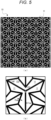
- Fig. 5 is an explanatory view for explaining a pattern of the through holes 11 formed in the through hole formation step S11 according to Example 1.
- Fig. 5(a) is an explanatory view illustrating a state in which the plurality of through holes 11 is arranged.
- black regions indicate a portion of the through holes 11, and white regions remain as the underlying substrate 10.
- Fig. 5(b) is an explanatory view illustrating a state in which the through holes 11 of Fig. 5(a) are enlarged.
- white regions indicate a portion of the through holes 11, and black regions remain as the underlying substrate 10.
- Fig. 6 is an explanatory view for explaining the strained layer removal step S12 according to Example 1.
- the underlying substrate 10 having the through holes 11 formed in the through hole formation step S11 was housed in a SiC container 50, the SiC container 50 was housed in a TaC container 60, and they were heated under the following conditions.
- the SiC container 50 is a fitting container including an upper container 51 and a lower container 52 that can be fitted to each other.
- a gap 53 is formed in a fitting portion between the upper container 51 and the lower container 52, and the SiC container 50 can be exhausted (evacuated) from the gap 53.
- the SiC container 50 has an etching space 54 formed by making a part of the SiC container 50 arranged on the low temperature side of the temperature gradient face the underlying substrate 10 in a state where the underlying substrate 10 is arranged on the high temperature side of the temperature gradient.
- the etching space 54 is a space for transporting and etching Si atoms and C atoms from the underlying substrate 10 to the SiC container 50 using a temperature difference provided between the underlying substrate 10 and the bottom surface of the SiC container 50 as the driving force.
- the SiC container 50 includes a substrate holder 55 that holds the underlying substrate 10 in a hollow state to form the etching space 54.
- the substrate holder 55 may not be provided depending on a direction of the temperature gradient of a heating furnace. For example, when the heating furnace forms a temperature gradient such that the temperature becomes lower from the lower container 52 toward the upper container 51, the underlying substrate 10 may be disposed on the bottom surface of the lower container 52 without providing the substrate holder 55.
- the TaC container 60 is a fitting container including an upper container 61 and a lower container 62 that can be fitted to each other, and is configured to be able to house the SiC container 50.
- a gap 63 is formed in a fitting portion between the upper container 61 and the lower container 62, and the TaC container 60 can be exhausted (evacuated) from the gap 63.
- the TaC container 60 includes the Si vapor supply source 64 capable of supplying vapor pressure of a vapor phase type containing Si element into the TaC container 60.
- the Si vapor supply source 64 may be configured to generate vapor pressure of the vapor phase type containing Si element in the TaC container 60 during heat treatment.
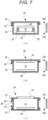
- Fig. 7 is an explanatory view for explaining the crystal growth step S20 according to Example 1.
- the underlying substrate 10 from which the strained layer 12 has been removed in the strained layer removal step S12 was housed in the crucible 30 while facing the semiconductor material 40, and was heated under the following conditions.
- the crucible 30 has a source transport space 31 between the underlying substrate 10 and the semiconductor material 40.
- the source is transported from the semiconductor material 40 onto the underlying substrate 10 through the source transport space 31.
- Fig. 7(a) is an example of the crucible 30 to be used in the crystal growth step S20.
- the crucible 30 is a fitting container including an upper container 32 and a lower container 33 that can be fitted to each other.
- a gap 34 is formed in a fitting portion between the upper container 32 and the lower container 33, and the crucible 30 can be exhausted (evacuated) from the gap 34.
- the crucible 30 includes a substrate holder 35 that forms the source transport space 31.
- the substrate holder 35 is provided between the underlying substrate 10 and the semiconductor material 40, and forms the source transport space 31 by arranging the semiconductor material 40 on the high temperature side and the underlying substrate 10 on the low temperature side.
- Figs. 7(b) and 7(c) are another example of the crucible 30 to be used in the crystal growth step S20.
- the temperature gradient in Figs. 7(b) and 7(c) is set opposite to the temperature gradient in Fig. 7(a) , and the underlying substrate 10 is disposed on an upper side.
- the semiconductor material 40 is disposed on the high temperature side, and the underlying substrate 10 is disposed on the low temperature side to form the source transport space 31.
- Fig. 7(b) illustrates an example in which the underlying substrate 10 is fixed to the upper container 32 side to form the source transport space 31 with the semiconductor material 40.
- Fig. 7(c) illustrates an example in which the source transport space 31 is formed between the semiconductor material 40 and the underlying substrate 10 by forming a through window in the upper container 32 and arranging the underlying substrate 10. Furthermore, as illustrated in Fig. 7(c) , an intermediate member 36 may be provided between the upper container 32 and the lower container 33 to form the source transport space 31.
- the AlN sintered body of the semiconductor material 40 was sintered in the following procedure.
- the AlN powder was placed in a frame of a TaC block and compacted with an appropriate force. Thereafter, the compacted AlN powder and the TaC block were housed in a thermal decomposition carbon crucible and heated under the following conditions.
- Fig. 7 is an SEM image of the underlying substrate 10 and the growth layer 20 cooled under the above conditions observed from the underlying substrate 10 side. It can be seen that the cracks 13 are formed in the underlying substrate 10.
- Example 1 The same underlying substrate 10 as in Example 1 was subjected to the crystal growth step S20 and the temperature lowering step S30 under the same conditions as in Example 1. In other words, in Comparative Example 1, the embrittlement processing step S10 was not performed, and the crystal growth step S20 was performed.
- the cracks 13 were not observed in the underlying substrate 10 of the semiconductor substrate manufactured according to Comparative Example 1.
- the cracks were observed at a crack linear density of 1.0 mm -1 .
- Example 1 From the results of Example 1 and Comparative Example 1, it can be understood that the stress generated in the growth layer 20 can be released to the underlying substrate 10 by reducing the strength of the underlying substrate 10 in the embrittlement processing step S10, and the occurrence of cracks in the growth layer 20 can be suppressed.
Landscapes
- Chemical & Material Sciences (AREA)
- Engineering & Computer Science (AREA)
- Materials Engineering (AREA)
- Organic Chemistry (AREA)
- Crystallography & Structural Chemistry (AREA)
- Metallurgy (AREA)
- Inorganic Chemistry (AREA)
- Ceramic Engineering (AREA)
- Manufacturing & Machinery (AREA)
- Structural Engineering (AREA)
- Chemical Kinetics & Catalysis (AREA)
- General Chemical & Material Sciences (AREA)
- Crystals, And After-Treatments Of Crystals (AREA)
Applications Claiming Priority (2)
| Application Number | Priority Date | Filing Date | Title |
|---|---|---|---|
| JP2020072547 | 2020-04-14 | ||
| PCT/JP2021/013743 WO2021210390A1 (ja) | 2020-04-14 | 2021-03-30 | 半導体基板の製造方法、半導体基板、及び、成長層におけるクラックの発生を抑制する方法 |
Publications (2)
| Publication Number | Publication Date |
|---|---|
| EP4137622A1 true EP4137622A1 (de) | 2023-02-22 |
| EP4137622A4 EP4137622A4 (de) | 2024-05-22 |
Family
ID=78084923
Family Applications (1)
| Application Number | Title | Priority Date | Filing Date |
|---|---|---|---|
| EP21788428.7A Pending EP4137622A4 (de) | 2020-04-14 | 2021-03-30 | Verfahren zur herstellung eines halbleitersubstrats, halbleitersubstrat und verfahren zur verhinderung des auftretens von rissen in einer wachstumsschicht |
Country Status (6)
| Country | Link |
|---|---|
| US (1) | US12540416B2 (de) |
| EP (1) | EP4137622A4 (de) |
| JP (1) | JP7769846B2 (de) |
| CN (1) | CN115398044B (de) |
| TW (1) | TWI885111B (de) |
| WO (1) | WO2021210390A1 (de) |
Families Citing this family (2)
| Publication number | Priority date | Publication date | Assignee | Title |
|---|---|---|---|---|
| SE546355C2 (en) * | 2022-11-28 | 2024-10-15 | Kiselkarbid I Stockholm Ab | Production of silicon carbide epitaxial wafers |
| WO2026071134A1 (ja) * | 2024-09-27 | 2026-04-02 | 学校法人関西学院 | 半導体基板を製造するライン、半導体基板の製造方法、半導体基板を検査する方法、半導体基板を加工する方法、及び半導体基板の加工を評価する方法 |
Family Cites Families (14)
| Publication number | Priority date | Publication date | Assignee | Title |
|---|---|---|---|---|
| CA2231625C (en) * | 1997-03-17 | 2002-04-02 | Canon Kabushiki Kaisha | Semiconductor substrate having compound semiconductor layer, process for its production, and electronic device fabricated on semiconductor substrate |
| JP2000311903A (ja) | 1999-04-27 | 2000-11-07 | Kyocera Corp | 化合物半導体基板およびその製造方法 |
| US6579359B1 (en) * | 1999-06-02 | 2003-06-17 | Technologies And Devices International, Inc. | Method of crystal growth and resulted structures |
| JP4072352B2 (ja) * | 2002-02-05 | 2008-04-09 | 住友電気工業株式会社 | 窒化物系化合物半導体素子及びその作製方法 |
| JP4088111B2 (ja) | 2002-06-28 | 2008-05-21 | 日立電線株式会社 | 多孔質基板とその製造方法、GaN系半導体積層基板とその製造方法 |
| JP6052570B2 (ja) | 2012-02-28 | 2016-12-27 | エア・ウォーター株式会社 | 半導体基板の製造方法 |
| JP6241286B2 (ja) * | 2014-01-14 | 2017-12-06 | 住友電気工業株式会社 | 炭化珪素単結晶の製造方法 |
| JP6183317B2 (ja) * | 2014-08-08 | 2017-08-23 | 豊田合成株式会社 | Iii族窒化物半導体の製造方法及びiii族窒化物半導体ウエハ |
| WO2016147786A1 (ja) * | 2015-03-18 | 2016-09-22 | 住友化学株式会社 | 窒化物半導体成長用基板及びその製造方法、並びに半導体デバイス及びその製造方法 |
| EP3450595B1 (de) * | 2016-04-28 | 2021-07-14 | Kwansei Gakuin Educational Foundation | Epitaktisches wachstumsverfahren in der dampfphase und verfahren zur herstellung eines substrats mit der epitaxialschicht |
| JP6949358B2 (ja) * | 2017-07-28 | 2021-10-13 | 学校法人関西学院 | 単結晶SiCの製造方法、SiCインゴットの製造方法、及びSiCウエハの製造方法 |
| CN109423694B (zh) | 2017-08-21 | 2022-09-09 | 株式会社Flosfia | 结晶膜、包括结晶膜的半导体装置以及制造结晶膜的方法 |
| FR3079532B1 (fr) | 2018-03-28 | 2022-03-25 | Soitec Silicon On Insulator | Procede de fabrication d'une couche monocristalline de materiau ain et substrat pour croissance par epitaxie d'une couche monocristalline de materiau ain |
| TWI896630B (zh) * | 2020-04-14 | 2025-09-11 | 學校法人關西學院 | 氮化鋁基板的製造方法、氮化鋁基板以及氮化鋁層中的裂痕產生的抑制方法 |
-
2021
- 2021-03-30 US US17/996,091 patent/US12540416B2/en active Active
- 2021-03-30 CN CN202180028129.1A patent/CN115398044B/zh active Active
- 2021-03-30 WO PCT/JP2021/013743 patent/WO2021210390A1/ja not_active Ceased
- 2021-03-30 JP JP2022515285A patent/JP7769846B2/ja active Active
- 2021-03-30 EP EP21788428.7A patent/EP4137622A4/de active Pending
- 2021-03-30 TW TW110111474A patent/TWI885111B/zh active
Also Published As
| Publication number | Publication date |
|---|---|
| US20230203704A1 (en) | 2023-06-29 |
| CN115398044A (zh) | 2022-11-25 |
| JPWO2021210390A1 (de) | 2021-10-21 |
| WO2021210390A1 (ja) | 2021-10-21 |
| TW202143303A (zh) | 2021-11-16 |
| CN115398044B (zh) | 2026-04-10 |
| TWI885111B (zh) | 2025-06-01 |
| JP7769846B2 (ja) | 2025-11-14 |
| EP4137622A4 (de) | 2024-05-22 |
| US12540416B2 (en) | 2026-02-03 |
Similar Documents
| Publication | Publication Date | Title |
|---|---|---|
| US9915011B2 (en) | Low resistivity single crystal silicon carbide wafer | |
| EP2059946B1 (de) | Mikroröhrchen-freies siliciumcarbid und verfahren zu seiner herstellung | |
| EP2245218B1 (de) | Verfahren zur herstellung von gruppe-iii-nitridwafer und gruppe-iii-nitridwafer | |
| US12540416B2 (en) | Method for manufacturing a semiconductor substrate and method for suppressing occurrence of cracks in a growth layer | |
| US12509795B2 (en) | Method for manufacturing aluminum nitride substrate, aluminum nitride substrate, and method for forming aluminum nitride layer | |
| EP4137616A1 (de) | Verfahren zur herstellung eines aluminiumnitridsubstrats, aluminiumnitridsubstrat und verfahren zur unterdrückung der einführung einer versetzung in eine aluminiumnitrid-wachstumsschicht | |
| US12385158B2 (en) | Method for manufacturing a semiconductor substrate by forming a growth layer on an underlying substrate having through holes | |
| EP4137614A1 (de) | Verfahren zur herstellung eines aluminiumnitridsubstrats, aluminiumnitridsubstrat und verfahren zur unterdrückung des auftretens von rissen in einer aluminiumnitridschicht | |
| US12460315B2 (en) | Method for manufacturing semiconductor substrates and method for suppressing introduction of displacement to growth layer |
Legal Events
| Date | Code | Title | Description |
|---|---|---|---|
| STAA | Information on the status of an ep patent application or granted ep patent |
Free format text: STATUS: THE INTERNATIONAL PUBLICATION HAS BEEN MADE |
|
| PUAI | Public reference made under article 153(3) epc to a published international application that has entered the european phase |
Free format text: ORIGINAL CODE: 0009012 |
|
| STAA | Information on the status of an ep patent application or granted ep patent |
Free format text: STATUS: REQUEST FOR EXAMINATION WAS MADE |
|
| 17P | Request for examination filed |
Effective date: 20221107 |
|
| AK | Designated contracting states |
Kind code of ref document: A1 Designated state(s): AL AT BE BG CH CY CZ DE DK EE ES FI FR GB GR HR HU IE IS IT LI LT LU LV MC MK MT NL NO PL PT RO RS SE SI SK SM TR |
|
| DAV | Request for validation of the european patent (deleted) | ||
| DAX | Request for extension of the european patent (deleted) | ||
| REG | Reference to a national code |
Ref country code: DE Ref legal event code: R079 Free format text: PREVIOUS MAIN CLASS: C30B0029380000 Ipc: C30B0029360000 |
|
| A4 | Supplementary search report drawn up and despatched |
Effective date: 20240422 |
|
| RIC1 | Information provided on ipc code assigned before grant |
Ipc: C30B 33/06 20060101ALI20240416BHEP Ipc: C30B 25/18 20060101ALI20240416BHEP Ipc: C30B 23/02 20060101ALI20240416BHEP Ipc: C30B 23/06 20060101ALI20240416BHEP Ipc: C30B 29/36 20060101AFI20240416BHEP |