EP4137799A1 - Optisches probendetektionssystem - Google Patents
Optisches probendetektionssystem Download PDFInfo
- Publication number
- EP4137799A1 EP4137799A1 EP22195116.3A EP22195116A EP4137799A1 EP 4137799 A1 EP4137799 A1 EP 4137799A1 EP 22195116 A EP22195116 A EP 22195116A EP 4137799 A1 EP4137799 A1 EP 4137799A1
- Authority
- EP
- European Patent Office
- Prior art keywords
- light
- excitation light
- dielectric member
- detection system
- sample detection
- Prior art date
- Legal status (The legal status is an assumption and is not a legal conclusion. Google has not performed a legal analysis and makes no representation as to the accuracy of the status listed.)
- Granted
Links
Images





Classifications
-
- G—PHYSICS
- G01—MEASURING; TESTING
- G01N—INVESTIGATING OR ANALYSING MATERIALS BY DETERMINING THEIR CHEMICAL OR PHYSICAL PROPERTIES
- G01N21/00—Investigating or analysing materials by the use of optical means, i.e. using sub-millimetre waves, infrared, visible or ultraviolet light
- G01N21/62—Systems in which the material investigated is excited whereby it emits light or causes a change in wavelength of the incident light
- G01N21/63—Systems in which the material investigated is excited whereby it emits light or causes a change in wavelength of the incident light optically excited
- G01N21/64—Fluorescence; Phosphorescence
- G01N21/645—Specially adapted constructive features of fluorimeters
- G01N21/648—Specially adapted constructive features of fluorimeters using evanescent coupling or surface plasmon coupling for the excitation of fluorescence
-
- G—PHYSICS
- G01—MEASURING; TESTING
- G01N—INVESTIGATING OR ANALYSING MATERIALS BY DETERMINING THEIR CHEMICAL OR PHYSICAL PROPERTIES
- G01N21/00—Investigating or analysing materials by the use of optical means, i.e. using sub-millimetre waves, infrared, visible or ultraviolet light
- G01N21/17—Systems in which incident light is modified in accordance with the properties of the material investigated
- G01N21/55—Specular reflectivity
- G01N21/552—Attenuated total reflection
- G01N21/553—Attenuated total reflection and using surface plasmons
-
- G—PHYSICS
- G01—MEASURING; TESTING
- G01N—INVESTIGATING OR ANALYSING MATERIALS BY DETERMINING THEIR CHEMICAL OR PHYSICAL PROPERTIES
- G01N21/00—Investigating or analysing materials by the use of optical means, i.e. using sub-millimetre waves, infrared, visible or ultraviolet light
- G01N21/62—Systems in which the material investigated is excited whereby it emits light or causes a change in wavelength of the incident light
- G01N21/63—Systems in which the material investigated is excited whereby it emits light or causes a change in wavelength of the incident light optically excited
- G01N21/64—Fluorescence; Phosphorescence
- G01N21/6428—Measuring fluorescence of fluorescent products of reactions or of fluorochrome labelled reactive substances, e.g. measuring quenching effects, using measuring "optrodes"
-
- G—PHYSICS
- G02—OPTICS
- G02B—OPTICAL ELEMENTS, SYSTEMS OR APPARATUS
- G02B5/00—Optical elements other than lenses
- G02B5/04—Prisms
Definitions
- the present invention relates to an optical sample detection system for detecting a measurement target substance included in a sensor chip using a surface plasmon resonance apparatus applying a surface plasmon resonance (SPR) phenomenon, a surface plasmon-field enhanced fluorescence spectroscopic apparatus based on principle of surface plasmon-field enhanced fluorescence spectroscopy (SPFS), or the like.
- SPR surface plasmon resonance
- SPFS surface plasmon-field enhanced fluorescence spectroscopic apparatus based on principle of surface plasmon-field enhanced fluorescence spectroscopy
- SPR apparatus a surface plasmon resonance apparatus
- SPR apparatus for example, for detecting an extremely minute analyte in a living body by applying a phenomenon (surface plasmon resonance (SPR) phenomenon) that obtains a high light output by resonance of electrons and light in a fine region at a nanometer level or the like.
- SPR surface plasmon resonance
- SPFS apparatus a surface plasmon-field enhanced fluorescence spectroscopic apparatus capable of detecting an analyte with higher accuracy than the SPR apparatus based on principle of surface plasmon-field enhanced fluorescence spectroscopy (SPFS) applying a surface plasmon resonance (SPR) phenomenon is also one of such sample detection apparatuses.
- SPFS apparatus surface plasmon-field enhanced fluorescence spectroscopic apparatus
- This surface plasmon-field enhanced fluorescence spectroscopy obtains an effect of enhancing an electric field of surface plasmon light by generating surface plasmon light (compressional wave) on a surface of a metal film under a condition that excitation light such as laser light emitted from a light source undergoes attenuated total reflectance (ATR) on the surface of the metal film to increase the amount of photons possessed by the excitation light emitted from the light source by dozens of times to several hundreds of times.
- excitation light such as laser light emitted from a light source undergoes attenuated total reflectance (ATR) on the surface of the metal film to increase the amount of photons possessed by the excitation light emitted from the light source by dozens of times to several hundreds of times.
- Fig. 13 is a schematic configuration diagram for explaining a configuration of a conventional SPFS system.
- a conventional SPFS system 100 includes a sensor chip 114 including a prism-shaped dielectric member 102 having a substantially trapezoidal vertical cross section, a metal film 104 formed on a horizontal upper surface 102a of the dielectric member 102, a reaction layer 106 formed on an upper surface of the metal film 104, and a channel forming member 110 and a channel lid member 112 forming a channel 108 so as to surround the reaction layer 106.
- the sensor chip 114 is loaded in a sensor chip loading portion 116 of an SPFS apparatus 101.
- the reaction layer 106 of the sensor chip 114 has a solid phase film for capturing an analyte labeled with a fluorescent substance. By feeding a sample liquid containing the analyte to the channel 108, the analyte can be fixed onto the metal film 104.
- a light receiving unit 120 of the SPFS apparatus 101 is disposed above the sensor chip 114 in order to measure the intensity of fluorescence 118 emitted by a fluorescent substance excited by surface plasmon light (compressional wave) generated on the metal film 104.
- a light source 122 of the SPFS apparatus 101 is disposed on one side surface (incidence surface 102b) side below the dielectric member 102. Excitation light 124 emitted from the light source 122 is incident on an incidence surface 102b of the dielectric member 102 from a lower portion of an outside of the dielectric member 102.
- the metal film 104 formed on the upper surface 102a of the dielectric member 102 is irradiated with the excitation light 124 through the dielectric member 102.
- the light amount of the fluorescence 118 is lower than the excitation light amount by about ten digits. Therefore, even if a small amount of the excitation light 124 is incident on the light receiving unit 120, an S/N ratio deteriorates, and detection accuracy deteriorates. Therefore, it is important to reduce stray light.
- the excitation light 124 is incident from the incidence surface 102b of the dielectric member 102, is then reflected by the metal film 104, and is emitted from an emission surface 102c of the dielectric member 102.
- a part of the excitation light 124 is reflected by the emission surface 102c of the dielectric member 102, and there is emission surface reflected light 124b emitted from the incidence surface 102b of the dielectric member 102.
- the emission surface reflected light 124b when the emission surface reflected light 124b is incident on the channel lid member 112, the emission surface reflected light 124b becomes light guided in the channel lid member 112. If the emission surface reflected light 124b exists in a visual field range of the light receiving unit 120, autofluorescence in the channel lid member 112 is detected, leading to deterioration of an S/N ratio.
- the emission surface reflected light 124b usually has a light amount of about 4% of the excitation light 124, and this amount is sufficiently large with respect to the fluorescence 118. Therefore, the emission surface reflected light 124b can be said to be stray light to be removed.
- a light absorbing portion 126 for absorbing metal film reflected light reflected by the metal film 104 is disposed in an optical path of the dielectric member 102.
- Patent Literature 2 as illustrated in Fig. 15 , by disposing an excitation light cut filter (wavelength filter) 128 for removing scattered light and reflected light in the sensor chip 114 on an upper surface of the sensor chip 114, the excitation light 124 is cut.
- an excitation light cut filter wavelength filter
- the metal film reflected light is not 100% absorbed by the light absorbing portion 126, minute reflected light exists in the light absorbing portion 126, and such reflected light stray light cannot be removed completely.
- an object of the present invention is to provide an optical sample detection system capable of measuring a sample with high accuracy by removing stray light incident on a lid member such as a channel lid member and preventing light derived from excitation light and having a larger light amount than fluorescence from existing in a visual field range of a light receiving unit.
- an optical sample detection system reflecting one aspect of the present invention includes: a sensor chip including:
- the present invention is designed such that emission surface reflected light derived from excitation light having a larger light amount than fluorescence is not incident on a lid member. Therefore, the emission surface reflected light is not guided into the lid member, an S/N ratio can be largely improved, and a sample can be measured with high accuracy.
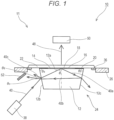
- Fig. 1 is a schematic view schematically illustrating an outline of an SPFS system as an aspect of an optical sample detection system of the present invention.
- Fig. 2 is a schematic view of a part of the SPFS system of Fig. 1 as seen from a bottom side.
- An SPFS system 10 includes a sensor chip 24 including a prism-shaped dielectric member 12 having a substantially trapezoidal vertical cross section, a metal film 14 formed on a horizontal upper surface 12a of the dielectric member 12, a reaction layer 16 formed on an upper surface of the metal film 14, and a channel forming member 20 and a channel lid member 22 forming a channel 18 so as to surround the reaction layer 16.
- the sensor chip 24 is loaded in a chip loading portion 26 of an SPFS apparatus 11.
- the reaction layer 16 of the sensor chip 24 has a solid phase film for thinning an analyte labeled with a fluorescent substance. By feeding a sample liquid containing the analyte to the channel 18, the analyte can be fixed onto the metal film 14.
- the solid phase film is obtained by fixing a ligand for capturing an analyte, and can be constituted, for example, by a self-assembled monolayer (SAM) and a solid-phasing layer formed on the SAM
- SAM self-assembled monolayer
- the solid-phasing layer preferably includes a polymer constituted by at least one monomer selected from the group consisting of monomers included in glucose, carboxymethylated glucose, a vinyl ester, an acrylic acid ester, a methacrylic acid ester, an olefin, a styrene, a crotonic acid ester, an itaconic acid diester, a maleic acid diester, a fumaric acid diester, an allyl compound, a vinyl ether, and a vinyl ketone, and more preferably includes a hydrophilic polymer such as dextran or a dextran derivative and a hydrophobic polymer constituted by a hydrophobic monomer included in a vinyl ester, an acrylic acid ester, a methacrylic acid ester, an olefin, a styrene, a crotonic acid ester, an itaconic acid diester, a maleic acid diester, a fumaric acid diester, an
- the dielectric member 12 is not particularly limited as long as being optically transparent at least with respect to the excitation light 40. However, in order to obtain a sensor chip which is inexpensive and excellent in a handling property, the dielectric member 12 is made of a resin material by injection molding.
- Examples of the resin material forming the dielectric member 12 include a polyester such as polyethylene terephthalate (PET) or polyethylene naphthalate, a polyolefin such as polyethylene (PE) or polypropylene (PP), a polycyclic olefin such as a cyclic olefin copolymer (COC) or a cyclic olefin polymer (COP), a vinyl-based resin such as polyvinyl chloride or polyvinylidene chloride, polystyrene, polyetheretherketone (PEEK), polysulfone (PSF), polyethersulfone (PES), polycarbonate (PC), polyamide, polyimide, an acrylic resin, and triacetylcellulose (TAC).
- PET polyethylene terephthalate
- PP polyethylene naphthalate
- a polyolefin such as polyethylene (PE) or polypropylene (PP)
- a polycyclic olefin such as
- the metal film 14 is not particularly limited, but is preferably made of at least one metal selected from the group consisting of gold, silver, aluminum, copper, and platinum, more preferably made of gold, and furthermore, may be made of an alloy of these metals.
- such a metal is suitable for the metal film 14 because of being stable to oxidation and increasing an electric field enhancement effect due to surface plasmon light (compressional wave) as described later.
- a method for forming the metal film 14 is not particularly limited, and examples thereof include a sputtering method, a vapor deposition method (a resistance heating vapor deposition method, an electron beam vapor deposition method, or the like), an electrolytic plating method, and an electroless plating method.
- a sputtering method or a vapor deposition method is preferably used in view of easiness in adjustment of thin film forming conditions.
- the thickness of the metal film 14 is not particularly limited, but is preferably within a range of 5 nm to 500 nm. Note that it is more preferable to use gold within a range of 20 nm to 70 nm, silver within a range of 20 nm to 70 nm, aluminum within a range of 10 to 50 nm, copper within a range of 20 to 70 nm, platinum within a range of 20 to 70 nm, and an alloy of these metals within a range of 10 to 70 nm from a viewpoint of the electric field enhancement effect.
- the thickness of the metal film 14 within the above range is preferable because surface plasmon light (compressional wave) is easily generated.
- the shape of the metal film 14 is not particularly limited as long as the metal film 14 has such a thickness.
- an acrylic pressure-sensitive adhesive sheet or the like having a channel groove with a predetermined width and a predetermined length punched can be used as the channel forming member 20, for example, an acrylic pressure-sensitive adhesive sheet or the like having a channel groove with a predetermined width and a predetermined length punched can be used as the channel forming member 20, for example, an acrylic pressure-sensitive adhesive sheet or the like having a channel groove with a predetermined width and a predetermined length punched can be used.
- the thickness of such an acrylic pressure-sensitive adhesive sheet is not particularly limited, but is preferably about 0.1 mm
- channel lid member 22 is not particularly limited as long as being a material having translucency with respect to the excitation light 40 and fluorescence 48, but a similar resin material to the above-described dielectric member 12 can be used.
- the channel lid member 22 includes a sample inflow port 28 and a sample discharge port 30 for feeding a sample liquid containing an analyte to the channel 18.
- a circulation feeding unit such as a pump, the sample liquid can be circulated and fed in one direction.
- a liquid reservoir 32 at the sample discharge port 30, injecting a sample liquid into the sample inflow port 28, for example, using a pipette, and repeating suction/injection of the sample liquid with the pipette, the sample liquid can be reciprocated in the pipette, the channel 18, and the liquid reservoir 32, and an analyte in the sample liquid is captured rapidly and efficiently by the ligand fixed to a solid phase film.
- the sample liquid can be reciprocated in the pipette, the channel 18, and the liquid reservoir 32, and an analyte in the sample liquid is captured rapidly and efficiently by the ligand fixed to a solid phase film.
- the reaction layer 16 is disposed in the channel 18, and a sample liquid is fed to the channel 18.
- the reaction layer 16 may be disposed in a well portion 19 such that the sample liquid stays in the well portion 19.
- a well lid member 23 is used in place of the channel lid member 22.
- the width of the channel lid member 22 is designed so as to be larger than the width of the dielectric member 12 in the optical path cross section of the excitation light 40.
- a holding region 34 can be provided in the channel lid member 22, and the sensor chip 24 can be loaded in the chip loading portion 26 such that the holding region 34 is in contact with the chip holding unit 36 of the chip loading portion 26.
- the "optical path cross section” means a cross section which coincides with a plane including an optical path of the excitation light 40 (including optical paths of metal film reflected light 40a and emission surface reflected light 40c described later) in a case where the excitation light 40 is emitted from a light projecting unit 38 toward the metal film 14.
- the light projecting unit 38 of the SPFS apparatus 11 for emitting the excitation light 40 is disposed on one side surface side below the sensor chip 24.
- the light projecting unit 38 includes a light source including, for example, a laser diode (LD), a light emitting diode (LED), or a high intensity discharge (HID) lamp, and a collimating lens for converting light emitted from the light source into a parallel light flux.
- a light source including, for example, a laser diode (LD), a light emitting diode (LED), or a high intensity discharge (HID) lamp, and a collimating lens for converting light emitted from the light source into a parallel light flux.
- LD laser diode
- LED light emitting diode
- HID high intensity discharge
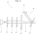
- Fig. 5 is a schematic view illustrating an example of an optical configuration of the light projecting unit 38 in the SPFS system 10 according to the present embodiment.
- an optical system of the light projecting unit 38 includes a laser diode (LD) 54 as a light source, a collimating lens 56 for collimating light emitted from the LD 54, a polarizing plate 58 for converting the excitation light 40 emitted to the metal film 14 of the sensor chip 24 into P-polarized light, a short pass filter 60 for cutting light with a certain wavelength for preventing scattered light or stray light of the LD 54 from being detected by a light receiving unit 50, and an aperture 62 for regulating an irradiation spot size onto the metal film 14.
- LD laser diode
- the excitation light 40 emitted from such light projecting unit 38 is substantially parallel light.
- an emission wavelength of the LD 54 includes at least a wavelength for generating surface plasmon on the metal film 14.
- an auto power control (APC) optical system 64 is disposed in the light projecting unit 38 in order to keep the light amount emitted from the light projecting unit 38 constant.
- the APC optical system 64 includes an APC photodiode 66 and a beam splitter 68 for causing a part of the excitation light 40 emitted from the aperture 62 to be reflected by the APC photodiode 66 and emitting remaining light to the metal film 14.
- a control unit By detecting the light amount of the light reflected by the beam splitter 68 in the APC photodiode 66 and applying feedback to an input current value of the LD 54 according to the detected light amount, a control unit (not illustrated) performs control such that the light amount detected by the APC photodiode 66 is constant, that is, the light amount emitted from the light projecting unit 38 is constant.
- the beam splitter 68 is desirably made of, for example, a high refractive index material having a refractive index of 1.6 or more.
- An incidence angle of the excitation light 40 on the beam splitter 68 is desirably smaller, and is desirably 40° or less, for example.
- an optical element such as the LD 54 or the collimating lens 56 in the light projecting unit 38 is eccentric due to a change in environment or time.
- the incidence angle of the excitation light 40 on the beam splitter 68 changes, the amount of variation in a reflection/transmission branching ratio of the beam splitter 68 can be suppressed to a low value. Therefore, the light amount emitted from the light projecting unit 38 can be stabilized.
- the light projecting unit 38 includes an irradiation angle varying mechanism (not illustrated) such that the incidence angle of the excitation light 40 on the metal film 14 can be changed within a range of a predetermined measurement scanning angle.
- the measurement scanning angle means an emission angle of the emitted excitation light 40 obtained by scanning the light projecting unit 38 (zero reference of the angle is a line perpendicular to the plane of the metal film 14) while the light projecting unit 38 emits the excitation light 40 and the light receiving unit 50 measures the fluorescence 48 or scattered light such as plasmon scattered light, or both the fluorescence 48 and the scattered light.
- the plasmon scattered light is light in which surface plasmon itself generated on the metal film 14 is scattered, and the wavelength thereof is equal to the wavelength of the excitation light 40.
- an angle at which the light amount of plasmon scattered light is maximized is an enhancement angle, and intense fluorescence intensity by surface plasmon is obtained at an angle near this enhancement angle.
- the enhancement angle depends on the shape and refractive index of the dielectric member 12 in the sensor chip 24, the material and film thickness of the metal film 14, the refractive index of a fluid in the channel 18, and the like. Therefore, considering an error in manufacturing the sensor chip 24, an optimum enhancement angle is desirably obtained for each measurement.
- the excitation light 40 is emitted from the light projecting unit 38 toward the incidence surface 12b of the dielectric member 12 and is incident on the metal film 14 adjacent to an upper surface of the dielectric member 12.
- the fluorescence 48 emitted by a fluorescent substance excited by surface plasmon light (compressional wave) generated on the metal film 14 is detected by the light receiving unit 50 disposed above the sensor chip 24.
- an optical system of the light receiving unit 50 includes a photodiode which is a light receiving element for receiving scattered light (plasmon scattered light) generated by surface plasmon or the fluorescence 48, a lens for concentrating light on the photodiode, and an excitation light cut filter for cutting light having a wavelength of the excitation light 40.
- a photodiode which is a light receiving element for receiving scattered light (plasmon scattered light) generated by surface plasmon or the fluorescence 48
- a lens for concentrating light on the photodiode
- an excitation light cut filter for cutting light having a wavelength of the excitation light 40.
- the excitation light cut filter is disposed on an optical path in the light receiving unit 50.
- at least a part of the excitation light cut filter is retracted from the optical path in the light receiving unit 50, for example, using an excitation light cut filter driving mechanism such that the plasmon scattered light can be incident on a photodiode.
- the excitation light cut filter is, for example, a band pass filter made of a dielectric multilayer film, and is disposed at a position where the fluorescence 48 is a substantially parallel light flux in the optical path in the light receiving unit 50.
- the light receiving element is not limited to a photodiode as long as being able to measure the light amount of received light, such as a photomultiplier tube or an avalanche photodiode (APD).
- a photodiode such as a photomultiplier tube or an avalanche photodiode (APD).
- a part of the metal film reflected light 40a is reflected by the emission surface 12c.
- the emission surface reflected light 40b travels straight toward the incidence surface 12b, and is emitted from the incidence surface 12b to an outside of the dielectric member 12.
- the emission surface reflected light 40b is not incident on the channel lid member 22 within a measurement scanning angle.
- Fig. 6 is a flow chart for explaining a flow of measurement in the SPFS system according to the present embodiment.
- the sensor chip 24 is prepared and attached to the chip loading portion 26 of the SPFS system 10.
- the sensor chip 24 is exchanged and disposable for each sample in a biochemical test. In general, blood or the like is used as a sample.
- an enhancement angle is measured.
- scanning is performed for an emission angle of the excitation light 40 emitted from the light projecting unit 38, plasmon scattered light is detected by the light receiving unit 50, and the enhancement angle is obtained.
- an excitation light cut filter used in measurement of fluorescence described later is retracted from an optical path in the light receiving unit 50.
- the plasmon scattered light having the same wavelength as the excitation light 40 can reach the light receiving element in the light receiving unit 50, and the light amount of the plasmon scattered light can be measured by the light receiving unit 50.
- an excitation light cut filter is disposed in the optical path in the light receiving unit 50, the light projecting unit 38 emits the excitation light 40, the light amount detected by the light receiving unit 50 is measured, and this light amount is recorded as an optical blank value (oB).
- the angle of the light projecting unit 38 is set such that the emission angle of the excitation light 40 is the enhancement angle obtained by the measurement of the enhancement angle.
- a fluorescently labeling liquid is introduced into the channel 18, and a fluorescently labeling antibody contained in the fluorescently labeling liquid is brought into contact with and binding to an analyte to perform a fluorescently labeling reaction (secondary reaction).
- a fluorescently labeling reaction secondary reaction
- the analyte is fluorescently labeled.
- an inside of the channel 18 is cleaned in order to remove the excessive fluorescently labeling antibody.
- the angle of the light projecting unit 38 is set such that the emission angle of the excitation light 40 is an enhancement angle.
- the excitation light 40 is emitted while an excitation light cut filter is disposed on an optical path in the light receiving unit 50, and a fluorescence signal value (S) detected by the light receiving unit 50 is measured.
- a measurer may manually perform work such as movement of the sensor chip 24, the excitation light cut filter, or the like, or introduction, suction, cleaning, or the like of a sample liquid into the channel 18, or the SPFS system 10 may include a driving mechanism or a control mechanism for automatically performing the work.
- the SPFS system 10 may include a recording unit that records measurement results or an output unit that outputs results.
- Fig. 7 is a schematic view illustrating an example of the shape of a dielectric member in the SPFS system according to the present embodiment.
- the incidence surface 12b and the emission surface 12c are each a smooth surface, and an angle ⁇ a formed by the upper surface 12a adjacent to the metal film 14 of the dielectric member 12 and the incidence surface 12b is the same as an angle ⁇ b formed by the upper surface 12a adjacent to the metal film 14 of the dielectric member 12 and the emission surface 12c.
- ⁇ a is different from ⁇ b .
- ⁇ a is smaller than ⁇ b .
- the metal film reflected light 40a is reflected by the emission surface 12c, then is reflected by the upper surface 12a, and is emitted from the incidence surface 12b.
- the emission surface reflected light 40b reflected by the upper surface 12a does not travel toward a side of the channel lid member 22 in this manner. Therefore, it is possible to prevent the emission surface reflected light 40b from being incident on the channel lid member 22 within a measurement scanning angle.
- ⁇ a is larger than ⁇ b and is an obtuse angle.
- the metal film reflected light 40a is reflected by the emission surface 12c and then emitted from a bottom surface 12d.
- the emission surface 12c may be constituted by a plurality of surfaces. In this case, it is possible to prevent the emission surface reflected light 40b from being incident on the channel lid member 22 as long as ⁇ a is larger than ⁇ b similarly to Fig. 7(b) .
- ⁇ a By setting ⁇ a to an angle larger than ⁇ b in this manner, as illustrated in Fig. 6 , the emission surface reflected light 40b travelling toward the incidence surface 12b is closer to the bottom surface 12d. Therefore, it is easier to constitute the sensor chip 24.
- the emission surface reflected light 40b on the bottom surface 12d may travel toward the incidence surface 12b to be incident on the channel lid member 22. Therefore, it is preferable to prevent the emission surface reflected light 40b from travelling from the bottom surface 12d of the dielectric member 12 toward the incidence surface 12b by making the bottom surface 12d a scattering surface or a non-flat surface.
- the dielectric member 12 so as to satisfy the following formula (1) in at least a part within a measurement scanning angle of the excitation light 40, the emission surface reflected light 40b on the incidence surface 12b is emitted to a bottom surface side rather than in a horizontal direction, and the emission surface reflected light 40b can be prevented from being incident on the channel lid member 22.
- n 1 represents the refractive index of the dielectric member 12
- n 0 represents the refractive index of the dielectric member 12 on an excitation light incident side of the incidence surface 12b
- ⁇ represents the incidence angle of the excitation light 40 on the metal film 14.
- the emission angle ⁇ c of the emission surface reflected light 40b on the incidence surface 12b preferably coincides with a reflection angle ⁇ d of the incidence surface reflected light 40c on the incidence surface 12b within the measurement scanning angle of the excitation light 40.
- the range of the emission angle ⁇ c of the emission surface reflected light 40b overlaps with the range of the reflection angle ⁇ d of the incidence surface reflected light 40c within the measurement scanning angle of the excitation light 40. Therefore, a light existence range through which the emission surface reflected light 40b and the incidence surface reflected light 40c pass is narrowed, and the sensor chip 24 is easily configured such that the emission surface reflected light 40b and the incidence surface reflected light 40c are not incident on the channel lid member 22.
- Fig. 9 illustrates a relationship between an incidence angle of the excitation light 40 and each of the emission angle ⁇ c of the emission surface reflected light 40b on an incidence surface and the reflection angle ⁇ d of the incidence surface reflected light 40c in a case where the measurement scanning angle of the excitation light 40 is set to 60° to 72°.
- Fig. 10 illustrates a relationship between an incidence angle of the excitation light 40 and each of the emission angle ⁇ c of the emission surface reflected light 40b on an incidence surface and the reflection angle ⁇ d of the incidence surface reflected light 40c in a case where the measurement scanning angle of the excitation light 40 is set to 61° to 73°.
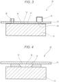
- a cut-out portion 22a can be formed in a part of the channel lid member 22 in an optical path cross section of the excitation light 40.
- the holding region 34 can be provided in the channel lid member 22, and the emission surface reflected light 40b is not incident on the channel lid member 22.
- the emission surface reflected light 40b emitted from the dielectric member 12 may be reflected, for example, by a wall surface of the SPFS system 10, causing stray light. Therefore, as illustrated in Fig. 1 , it is preferable to dispose a light shielding member 52 for absorbing the emission surface reflected light 40b emitted from the incidence surface 12b of the dielectric member 12 or for reflecting the emission surface reflected light 40b in a direction having no influence.
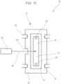
- Fig. 12 is a schematic view schematically illustrating another example of the SPFS system according to an aspect of the optical sample detection system of the present invention.
- the SPFS system 10 has a similar configuration to the SPFS system 10 illustrated in Fig. 1 . Therefore, the same constituent members are denoted by the same reference numerals, and a detailed description thereof will be omitted.
- the sensor chip 24 includes a reagent well 42 made of a material having translucency with respect to the excitation light 40.
- the reagent well 42 is, for example, a container for storing a sample liquid or a chemical liquid.
- the sensor chip 24 is loaded in a sensor chip loading hole 44 formed in the reagent well 42.
- a positional relation between the sensor chip 24 and the light projecting unit 38 can be kept constant to reduce a measurement error.
- the reagent well 42 made of a material having translucency with respect to the excitation light 40 is included in this manner, a configuration that the emission surface reflected light 40b is not incident on the channel lid member 22 and furthermore is not incident on the reagent well 42 in the measurement scanning angle of the excitation light 40 is preferable.
- the shape of the dielectric member 12 such as the angle ⁇ a or ⁇ b such that the emission surface reflected light 40b is not incident on the reagent well 42.
- a cut-out portion 42a may be formed in a part of the reagent well 42 in an optical path cross section of the excitation light 40.
- the holding region 46 can be provided in the reagent well 42, and the emission surface reflected light 40b is not incident on the reagent well 42.
- an SPFS system has been exemplified as an aspect of an optical sample detection system.
- various modifications are possible without departing from an object of the present invention, for example, the present invention is applicable to an SPR system as another aspect.
- the present invention can perform sample detection rapidly with high accuracy in a field requiring highly accurate detection such as a clinical test such as a blood test, for example, using surface plasmon-field enhanced fluorescence spectroscopy (SPFS).
- SPFS surface plasmon-field enhanced fluorescence spectroscopy
Landscapes
- Health & Medical Sciences (AREA)
- Physics & Mathematics (AREA)
- Chemical & Material Sciences (AREA)
- Immunology (AREA)
- General Physics & Mathematics (AREA)
- Analytical Chemistry (AREA)
- Life Sciences & Earth Sciences (AREA)
- Biochemistry (AREA)
- General Health & Medical Sciences (AREA)
- Pathology (AREA)
- Nuclear Medicine, Radiotherapy & Molecular Imaging (AREA)
- Optics & Photonics (AREA)
- Chemical Kinetics & Catalysis (AREA)
- Investigating, Analyzing Materials By Fluorescence Or Luminescence (AREA)
- Automatic Analysis And Handling Materials Therefor (AREA)
- Investigating Or Analysing Materials By Optical Means (AREA)
Applications Claiming Priority (3)
| Application Number | Priority Date | Filing Date | Title |
|---|---|---|---|
| JP2015221070 | 2015-11-11 | ||
| EP16864007.6A EP3376208A4 (de) | 2015-11-11 | 2016-10-25 | Optisches probendetektionssystem |
| PCT/JP2016/081592 WO2017082043A1 (ja) | 2015-11-11 | 2016-10-25 | 光学式検体検出システム |
Related Parent Applications (1)
| Application Number | Title | Priority Date | Filing Date |
|---|---|---|---|
| EP16864007.6A Division EP3376208A4 (de) | 2015-11-11 | 2016-10-25 | Optisches probendetektionssystem |
Publications (2)
| Publication Number | Publication Date |
|---|---|
| EP4137799A1 true EP4137799A1 (de) | 2023-02-22 |
| EP4137799B1 EP4137799B1 (de) | 2024-08-28 |
Family
ID=58695356
Family Applications (3)
| Application Number | Title | Priority Date | Filing Date |
|---|---|---|---|
| EP22195116.3A Active EP4137799B1 (de) | 2015-11-11 | 2016-10-25 | Optisches probendetektionssystem |
| EP16864007.6A Withdrawn EP3376208A4 (de) | 2015-11-11 | 2016-10-25 | Optisches probendetektionssystem |
| EP22192526.6A Withdrawn EP4191235A1 (de) | 2015-11-11 | 2016-10-25 | Optisches probendetektionssystem |
Family Applications After (2)
| Application Number | Title | Priority Date | Filing Date |
|---|---|---|---|
| EP16864007.6A Withdrawn EP3376208A4 (de) | 2015-11-11 | 2016-10-25 | Optisches probendetektionssystem |
| EP22192526.6A Withdrawn EP4191235A1 (de) | 2015-11-11 | 2016-10-25 | Optisches probendetektionssystem |
Country Status (5)
| Country | Link |
|---|---|
| US (1) | US10648914B2 (de) |
| EP (3) | EP4137799B1 (de) |
| JP (1) | JP6766820B2 (de) |
| ES (1) | ES2990007T3 (de) |
| WO (1) | WO2017082043A1 (de) |
Families Citing this family (4)
| Publication number | Priority date | Publication date | Assignee | Title |
|---|---|---|---|---|
| GB2565074A (en) * | 2017-07-31 | 2019-02-06 | Univ Bristol | Method and apparatus for bacterial analysis |
| WO2019064754A1 (ja) * | 2017-09-26 | 2019-04-04 | コニカミノルタ株式会社 | 分析方法および分析装置 |
| JP2020204540A (ja) * | 2019-06-18 | 2020-12-24 | 矢崎総業株式会社 | 金属の腐食検出装置及び腐食検出方法 |
| GB2619247B (en) * | 2021-03-26 | 2026-03-25 | Hamamatsu Photonics Kk | Attenuated total reflectance spectroscopy apparatus, and attenuated total reflectance spectroscopy method |
Citations (9)
| Publication number | Priority date | Publication date | Assignee | Title |
|---|---|---|---|---|
| US20020126290A1 (en) * | 2001-01-25 | 2002-09-12 | Fuji Photo Film Co., Ltd. | Sensor utilizing attenuated total reflection |
| WO2002073171A1 (en) * | 2001-03-14 | 2002-09-19 | Biacore Ab | Apparatus and method for total internal reflection spectroscopy |
| US20100225915A1 (en) * | 2009-03-04 | 2010-09-09 | Korea Advanced Institute Of Science And Technology | Prism for inducing Brewster's angle transmission and fluorescence detection apparatus for improving signal-to-noise ratio using thereof |
| JP2012202911A (ja) | 2011-03-28 | 2012-10-22 | Fujifilm Corp | 分析チップ |
| US20130240734A1 (en) * | 2010-07-28 | 2013-09-19 | University Of Delaware | Apparatus and method for performing surface plasmon resonance (spr) spectroscopy with an infrared (ir) spectrometer |
| EP2672273A1 (de) * | 2011-01-31 | 2013-12-11 | Konica Minolta, Inc. | Inspektionschip und mit dem inspektionschip ausgestatteter inspektionschipsatz |
| US8665444B2 (en) * | 2010-03-31 | 2014-03-04 | Fujifilm Corporation | Optical member and surface plasmon resonance measuring apparatus |
| JP2014167479A (ja) | 2014-04-14 | 2014-09-11 | Konica Minolta Inc | 表面プラズモン増強蛍光センサおよび表面プラズモン増強蛍光センサに用いられるチップ構造体 |
| WO2015129615A1 (ja) * | 2014-02-25 | 2015-09-03 | コニカミノルタ株式会社 | 測定方法および測定装置 |
Family Cites Families (10)
| Publication number | Priority date | Publication date | Assignee | Title |
|---|---|---|---|---|
| WO2005095927A1 (ja) * | 2004-03-31 | 2005-10-13 | Omron Corporation | 局在プラズモン共鳴センサ及び検査装置 |
| JP2006308511A (ja) * | 2005-05-02 | 2006-11-09 | Canon Inc | 化学分析装置及びその分析方法 |
| JP2008102117A (ja) * | 2006-09-21 | 2008-05-01 | Fujifilm Corp | 表面プラズモン増強蛍光センサおよび蛍光検出方法 |
| JP2009204486A (ja) | 2008-02-28 | 2009-09-10 | Fujifilm Corp | センシング装置及び物質検出方法 |
| JP5450993B2 (ja) * | 2008-07-14 | 2014-03-26 | 富士フイルム株式会社 | 検出方法、検出用試料セルおよび検出用キット |
| JP2010139332A (ja) | 2008-12-10 | 2010-06-24 | Beckman Coulter Inc | 自動分析装置 |
| US8163561B2 (en) * | 2009-11-30 | 2012-04-24 | Corning Incorporated | Method for depth resolved sensing of biological entities based on surface plasmon resonance sensors |
| US8243276B2 (en) * | 2009-11-30 | 2012-08-14 | Corning Incorporated | Variable penetration depth biosensor |
| WO2013099871A1 (ja) * | 2011-12-26 | 2013-07-04 | コニカミノルタ株式会社 | Spfs測定用センサーチップ、およびspfs測定用センサーチップを用いたspfs測定方法、ならびにspfs測定用センサーチップを備えたspfs測定装置 |
| JP2014032148A (ja) | 2012-08-06 | 2014-02-20 | Arkray Inc | 表面プラズモン励起増強蛍光取得構造体および表面プラズモン励起増強蛍光測定システム |
-
2016
- 2016-10-25 EP EP22195116.3A patent/EP4137799B1/de active Active
- 2016-10-25 ES ES22195116T patent/ES2990007T3/es active Active
- 2016-10-25 US US15/773,910 patent/US10648914B2/en active Active
- 2016-10-25 EP EP16864007.6A patent/EP3376208A4/de not_active Withdrawn
- 2016-10-25 EP EP22192526.6A patent/EP4191235A1/de not_active Withdrawn
- 2016-10-25 JP JP2017550049A patent/JP6766820B2/ja not_active Expired - Fee Related
- 2016-10-25 WO PCT/JP2016/081592 patent/WO2017082043A1/ja not_active Ceased
Patent Citations (10)
| Publication number | Priority date | Publication date | Assignee | Title |
|---|---|---|---|---|
| US20020126290A1 (en) * | 2001-01-25 | 2002-09-12 | Fuji Photo Film Co., Ltd. | Sensor utilizing attenuated total reflection |
| WO2002073171A1 (en) * | 2001-03-14 | 2002-09-19 | Biacore Ab | Apparatus and method for total internal reflection spectroscopy |
| US20100225915A1 (en) * | 2009-03-04 | 2010-09-09 | Korea Advanced Institute Of Science And Technology | Prism for inducing Brewster's angle transmission and fluorescence detection apparatus for improving signal-to-noise ratio using thereof |
| US8665444B2 (en) * | 2010-03-31 | 2014-03-04 | Fujifilm Corporation | Optical member and surface plasmon resonance measuring apparatus |
| US20130240734A1 (en) * | 2010-07-28 | 2013-09-19 | University Of Delaware | Apparatus and method for performing surface plasmon resonance (spr) spectroscopy with an infrared (ir) spectrometer |
| EP2672273A1 (de) * | 2011-01-31 | 2013-12-11 | Konica Minolta, Inc. | Inspektionschip und mit dem inspektionschip ausgestatteter inspektionschipsatz |
| JP2012202911A (ja) | 2011-03-28 | 2012-10-22 | Fujifilm Corp | 分析チップ |
| WO2015129615A1 (ja) * | 2014-02-25 | 2015-09-03 | コニカミノルタ株式会社 | 測定方法および測定装置 |
| US20170016823A1 (en) * | 2014-02-25 | 2017-01-19 | Konica Minolta, Inc. | Measurement method and measurement device |
| JP2014167479A (ja) | 2014-04-14 | 2014-09-11 | Konica Minolta Inc | 表面プラズモン増強蛍光センサおよび表面プラズモン増強蛍光センサに用いられるチップ構造体 |
Also Published As
| Publication number | Publication date |
|---|---|
| EP4137799B1 (de) | 2024-08-28 |
| JPWO2017082043A1 (ja) | 2018-08-30 |
| EP3376208A1 (de) | 2018-09-19 |
| EP3376208A4 (de) | 2019-02-20 |
| ES2990007T3 (es) | 2024-11-28 |
| WO2017082043A1 (ja) | 2017-05-18 |
| US10648914B2 (en) | 2020-05-12 |
| JP6766820B2 (ja) | 2020-10-14 |
| EP4191235A1 (de) | 2023-06-07 |
| US20180321152A1 (en) | 2018-11-08 |
Similar Documents
| Publication | Publication Date | Title |
|---|---|---|
| US20100273208A1 (en) | Microorganism testing apparatus | |
| JP5094484B2 (ja) | 蛍光検出方法および蛍光検出装置 | |
| EP3064929B1 (de) | Oberflächenplasmonresonanzfluoreszenzanalyseverfahren und oberflächenplasmonresonanzfluoreszenzanalysevorrichtung | |
| US10495576B2 (en) | Surface-plasmon enhanced fluorescence measurement method, surface-plasmon enhanced fluorescence measurement device, and analytical chip | |
| EP4137799B1 (de) | Optisches probendetektionssystem | |
| EP3321688B1 (de) | Erkennungsvorrichtung und erkennungsverfahren | |
| JP6587024B2 (ja) | 検出方法および検出装置 | |
| JPWO2018034143A1 (ja) | 測定方法、測定装置および測定システム | |
| JP6098523B2 (ja) | Spfs測定用センサーチップ、およびspfs測定用センサーチップを用いたspfs測定方法、ならびにspfs測定用センサーチップを備えたspfs測定装置 | |
| JPWO2018034208A1 (ja) | 測定方法 | |
| JPWO2018051863A1 (ja) | 測定方法 | |
| JP6922907B2 (ja) | 反応方法、ならびにこれを行う反応システムおよび反応装置 | |
| JP6631538B2 (ja) | 検出チップおよび検出方法 | |
| JPWO2014017433A1 (ja) | 光学式検体検出装置 | |
| JP7050776B2 (ja) | 検体検出装置及び検体検出方法 | |
| JPWO2019221040A1 (ja) | 検体検出チップ及びこれを用いた検体検出装置 | |
| JP6885458B2 (ja) | 検体検出システム用センサーチップ | |
| JP6658752B2 (ja) | 検出チップ、検出方法、検出装置および検出システム | |
| JPWO2014021171A1 (ja) | センサー部材の製造方法およびセンサーチップの製造方法ならびにセンサー部材の使用方法 | |
| WO2015076036A1 (ja) | 光学式検体検出装置 | |
| JP2017090349A (ja) | センサーチップおよびこのセンサーチップを備えた光学式検体検出システム |
Legal Events
| Date | Code | Title | Description |
|---|---|---|---|
| PUAI | Public reference made under article 153(3) epc to a published international application that has entered the european phase |
Free format text: ORIGINAL CODE: 0009012 |
|
| STAA | Information on the status of an ep patent application or granted ep patent |
Free format text: STATUS: THE APPLICATION HAS BEEN PUBLISHED |
|
| AC | Divisional application: reference to earlier application |
Ref document number: 3376208 Country of ref document: EP Kind code of ref document: P |
|
| AK | Designated contracting states |
Kind code of ref document: A1 Designated state(s): AL AT BE BG CH CY CZ DE DK EE ES FI FR GB GR HR HU IE IS IT LI LT LU LV MC MK MT NL NO PL PT RO RS SE SI SK SM TR |
|
| STAA | Information on the status of an ep patent application or granted ep patent |
Free format text: STATUS: REQUEST FOR EXAMINATION WAS MADE |
|
| 17P | Request for examination filed |
Effective date: 20230822 |
|
| RBV | Designated contracting states (corrected) |
Designated state(s): AL AT BE BG CH CY CZ DE DK EE ES FI FR GB GR HR HU IE IS IT LI LT LU LV MC MK MT NL NO PL PT RO RS SE SI SK SM TR |
|
| GRAP | Despatch of communication of intention to grant a patent |
Free format text: ORIGINAL CODE: EPIDOSNIGR1 |
|
| STAA | Information on the status of an ep patent application or granted ep patent |
Free format text: STATUS: GRANT OF PATENT IS INTENDED |
|
| INTG | Intention to grant announced |
Effective date: 20240402 |
|
| GRAS | Grant fee paid |
Free format text: ORIGINAL CODE: EPIDOSNIGR3 |
|
| GRAA | (expected) grant |
Free format text: ORIGINAL CODE: 0009210 |
|
| STAA | Information on the status of an ep patent application or granted ep patent |
Free format text: STATUS: THE PATENT HAS BEEN GRANTED |
|
| P01 | Opt-out of the competence of the unified patent court (upc) registered |
Free format text: CASE NUMBER: APP_38020/2024 Effective date: 20240626 |
|
| AC | Divisional application: reference to earlier application |
Ref document number: 3376208 Country of ref document: EP Kind code of ref document: P |
|
| AK | Designated contracting states |
Kind code of ref document: B1 Designated state(s): AL AT BE BG CH CY CZ DE DK EE ES FI FR GB GR HR HU IE IS IT LI LT LU LV MC MK MT NL NO PL PT RO RS SE SI SK SM TR |
|
| REG | Reference to a national code |
Ref country code: CH Ref legal event code: EP |
|
| REG | Reference to a national code |
Ref country code: DE Ref legal event code: R096 Ref document number: 602016089200 Country of ref document: DE |
|
| REG | Reference to a national code |
Ref country code: IE Ref legal event code: FG4D |
|
| REG | Reference to a national code |
Ref country code: ES Ref legal event code: FG2A Ref document number: 2990007 Country of ref document: ES Kind code of ref document: T3 Effective date: 20241128 |
|
| REG | Reference to a national code |
Ref country code: LT Ref legal event code: MG9D |
|
| PG25 | Lapsed in a contracting state [announced via postgrant information from national office to epo] |
Ref country code: NO Free format text: LAPSE BECAUSE OF FAILURE TO SUBMIT A TRANSLATION OF THE DESCRIPTION OR TO PAY THE FEE WITHIN THE PRESCRIBED TIME-LIMIT Effective date: 20241128 |
|
| REG | Reference to a national code |
Ref country code: AT Ref legal event code: MK05 Ref document number: 1718460 Country of ref document: AT Kind code of ref document: T Effective date: 20240828 |
|
| PG25 | Lapsed in a contracting state [announced via postgrant information from national office to epo] |
Ref country code: NL Free format text: LAPSE BECAUSE OF FAILURE TO SUBMIT A TRANSLATION OF THE DESCRIPTION OR TO PAY THE FEE WITHIN THE PRESCRIBED TIME-LIMIT Effective date: 20240828 Ref country code: GR Free format text: LAPSE BECAUSE OF FAILURE TO SUBMIT A TRANSLATION OF THE DESCRIPTION OR TO PAY THE FEE WITHIN THE PRESCRIBED TIME-LIMIT Effective date: 20241129 Ref country code: PL Free format text: LAPSE BECAUSE OF FAILURE TO SUBMIT A TRANSLATION OF THE DESCRIPTION OR TO PAY THE FEE WITHIN THE PRESCRIBED TIME-LIMIT Effective date: 20240828 Ref country code: FI Free format text: LAPSE BECAUSE OF FAILURE TO SUBMIT A TRANSLATION OF THE DESCRIPTION OR TO PAY THE FEE WITHIN THE PRESCRIBED TIME-LIMIT Effective date: 20240828 Ref country code: PT Free format text: LAPSE BECAUSE OF FAILURE TO SUBMIT A TRANSLATION OF THE DESCRIPTION OR TO PAY THE FEE WITHIN THE PRESCRIBED TIME-LIMIT Effective date: 20241230 |
|
| PG25 | Lapsed in a contracting state [announced via postgrant information from national office to epo] |
Ref country code: BG Free format text: LAPSE BECAUSE OF FAILURE TO SUBMIT A TRANSLATION OF THE DESCRIPTION OR TO PAY THE FEE WITHIN THE PRESCRIBED TIME-LIMIT Effective date: 20240828 |
|
| PG25 | Lapsed in a contracting state [announced via postgrant information from national office to epo] |
Ref country code: LV Free format text: LAPSE BECAUSE OF FAILURE TO SUBMIT A TRANSLATION OF THE DESCRIPTION OR TO PAY THE FEE WITHIN THE PRESCRIBED TIME-LIMIT Effective date: 20240828 |
|
| REG | Reference to a national code |
Ref country code: NL Ref legal event code: MP Effective date: 20240828 |
|
| PG25 | Lapsed in a contracting state [announced via postgrant information from national office to epo] |
Ref country code: IS Free format text: LAPSE BECAUSE OF FAILURE TO SUBMIT A TRANSLATION OF THE DESCRIPTION OR TO PAY THE FEE WITHIN THE PRESCRIBED TIME-LIMIT Effective date: 20241228 Ref country code: AT Free format text: LAPSE BECAUSE OF FAILURE TO SUBMIT A TRANSLATION OF THE DESCRIPTION OR TO PAY THE FEE WITHIN THE PRESCRIBED TIME-LIMIT Effective date: 20240828 |
|
| PG25 | Lapsed in a contracting state [announced via postgrant information from national office to epo] |
Ref country code: HR Free format text: LAPSE BECAUSE OF FAILURE TO SUBMIT A TRANSLATION OF THE DESCRIPTION OR TO PAY THE FEE WITHIN THE PRESCRIBED TIME-LIMIT Effective date: 20240828 |
|
| PG25 | Lapsed in a contracting state [announced via postgrant information from national office to epo] |
Ref country code: RS Free format text: LAPSE BECAUSE OF FAILURE TO SUBMIT A TRANSLATION OF THE DESCRIPTION OR TO PAY THE FEE WITHIN THE PRESCRIBED TIME-LIMIT Effective date: 20241128 |
|
| PG25 | Lapsed in a contracting state [announced via postgrant information from national office to epo] |
Ref country code: RS Free format text: LAPSE BECAUSE OF FAILURE TO SUBMIT A TRANSLATION OF THE DESCRIPTION OR TO PAY THE FEE WITHIN THE PRESCRIBED TIME-LIMIT Effective date: 20241128 Ref country code: PT Free format text: LAPSE BECAUSE OF FAILURE TO SUBMIT A TRANSLATION OF THE DESCRIPTION OR TO PAY THE FEE WITHIN THE PRESCRIBED TIME-LIMIT Effective date: 20241230 Ref country code: PL Free format text: LAPSE BECAUSE OF FAILURE TO SUBMIT A TRANSLATION OF THE DESCRIPTION OR TO PAY THE FEE WITHIN THE PRESCRIBED TIME-LIMIT Effective date: 20240828 Ref country code: NO Free format text: LAPSE BECAUSE OF FAILURE TO SUBMIT A TRANSLATION OF THE DESCRIPTION OR TO PAY THE FEE WITHIN THE PRESCRIBED TIME-LIMIT Effective date: 20241128 Ref country code: NL Free format text: LAPSE BECAUSE OF FAILURE TO SUBMIT A TRANSLATION OF THE DESCRIPTION OR TO PAY THE FEE WITHIN THE PRESCRIBED TIME-LIMIT Effective date: 20240828 Ref country code: LV Free format text: LAPSE BECAUSE OF FAILURE TO SUBMIT A TRANSLATION OF THE DESCRIPTION OR TO PAY THE FEE WITHIN THE PRESCRIBED TIME-LIMIT Effective date: 20240828 Ref country code: IS Free format text: LAPSE BECAUSE OF FAILURE TO SUBMIT A TRANSLATION OF THE DESCRIPTION OR TO PAY THE FEE WITHIN THE PRESCRIBED TIME-LIMIT Effective date: 20241228 Ref country code: HR Free format text: LAPSE BECAUSE OF FAILURE TO SUBMIT A TRANSLATION OF THE DESCRIPTION OR TO PAY THE FEE WITHIN THE PRESCRIBED TIME-LIMIT Effective date: 20240828 Ref country code: GR Free format text: LAPSE BECAUSE OF FAILURE TO SUBMIT A TRANSLATION OF THE DESCRIPTION OR TO PAY THE FEE WITHIN THE PRESCRIBED TIME-LIMIT Effective date: 20241129 Ref country code: FI Free format text: LAPSE BECAUSE OF FAILURE TO SUBMIT A TRANSLATION OF THE DESCRIPTION OR TO PAY THE FEE WITHIN THE PRESCRIBED TIME-LIMIT Effective date: 20240828 Ref country code: BG Free format text: LAPSE BECAUSE OF FAILURE TO SUBMIT A TRANSLATION OF THE DESCRIPTION OR TO PAY THE FEE WITHIN THE PRESCRIBED TIME-LIMIT Effective date: 20240828 Ref country code: AT Free format text: LAPSE BECAUSE OF FAILURE TO SUBMIT A TRANSLATION OF THE DESCRIPTION OR TO PAY THE FEE WITHIN THE PRESCRIBED TIME-LIMIT Effective date: 20240828 |
|
| PG25 | Lapsed in a contracting state [announced via postgrant information from national office to epo] |
Ref country code: SM Free format text: LAPSE BECAUSE OF FAILURE TO SUBMIT A TRANSLATION OF THE DESCRIPTION OR TO PAY THE FEE WITHIN THE PRESCRIBED TIME-LIMIT Effective date: 20240828 Ref country code: RO Free format text: LAPSE BECAUSE OF FAILURE TO SUBMIT A TRANSLATION OF THE DESCRIPTION OR TO PAY THE FEE WITHIN THE PRESCRIBED TIME-LIMIT Effective date: 20240828 Ref country code: DK Free format text: LAPSE BECAUSE OF FAILURE TO SUBMIT A TRANSLATION OF THE DESCRIPTION OR TO PAY THE FEE WITHIN THE PRESCRIBED TIME-LIMIT Effective date: 20240828 |
|
| PG25 | Lapsed in a contracting state [announced via postgrant information from national office to epo] |
Ref country code: EE Free format text: LAPSE BECAUSE OF FAILURE TO SUBMIT A TRANSLATION OF THE DESCRIPTION OR TO PAY THE FEE WITHIN THE PRESCRIBED TIME-LIMIT Effective date: 20240828 |
|
| PG25 | Lapsed in a contracting state [announced via postgrant information from national office to epo] |
Ref country code: CZ Free format text: LAPSE BECAUSE OF FAILURE TO SUBMIT A TRANSLATION OF THE DESCRIPTION OR TO PAY THE FEE WITHIN THE PRESCRIBED TIME-LIMIT Effective date: 20240828 |
|
| PG25 | Lapsed in a contracting state [announced via postgrant information from national office to epo] |
Ref country code: SK Free format text: LAPSE BECAUSE OF FAILURE TO SUBMIT A TRANSLATION OF THE DESCRIPTION OR TO PAY THE FEE WITHIN THE PRESCRIBED TIME-LIMIT Effective date: 20240828 |
|
| REG | Reference to a national code |
Ref country code: CH Ref legal event code: PL Ref country code: DE Ref legal event code: R097 Ref document number: 602016089200 Country of ref document: DE |
|
| PLBE | No opposition filed within time limit |
Free format text: ORIGINAL CODE: 0009261 |
|
| STAA | Information on the status of an ep patent application or granted ep patent |
Free format text: STATUS: NO OPPOSITION FILED WITHIN TIME LIMIT |
|
| PG25 | Lapsed in a contracting state [announced via postgrant information from national office to epo] |
Ref country code: MC Free format text: LAPSE BECAUSE OF FAILURE TO SUBMIT A TRANSLATION OF THE DESCRIPTION OR TO PAY THE FEE WITHIN THE PRESCRIBED TIME-LIMIT Effective date: 20240828 |
|
| PG25 | Lapsed in a contracting state [announced via postgrant information from national office to epo] |
Ref country code: BE Free format text: LAPSE BECAUSE OF NON-PAYMENT OF DUE FEES Effective date: 20241031 Ref country code: LU Free format text: LAPSE BECAUSE OF NON-PAYMENT OF DUE FEES Effective date: 20241025 |
|
| PG25 | Lapsed in a contracting state [announced via postgrant information from national office to epo] |
Ref country code: CH Free format text: LAPSE BECAUSE OF NON-PAYMENT OF DUE FEES Effective date: 20241031 |
|
| 26N | No opposition filed |
Effective date: 20250530 |
|
| REG | Reference to a national code |
Ref country code: BE Ref legal event code: MM Effective date: 20241031 |
|
| PG25 | Lapsed in a contracting state [announced via postgrant information from national office to epo] |
Ref country code: SE Free format text: LAPSE BECAUSE OF FAILURE TO SUBMIT A TRANSLATION OF THE DESCRIPTION OR TO PAY THE FEE WITHIN THE PRESCRIBED TIME-LIMIT Effective date: 20240828 |
|
| PGFP | Annual fee paid to national office [announced via postgrant information from national office to epo] |
Ref country code: IT Payment date: 20250923 Year of fee payment: 10 |
|
| PGFP | Annual fee paid to national office [announced via postgrant information from national office to epo] |
Ref country code: GB Payment date: 20250923 Year of fee payment: 10 |
|
| PGFP | Annual fee paid to national office [announced via postgrant information from national office to epo] |
Ref country code: FR Payment date: 20250924 Year of fee payment: 10 |
|
| PG25 | Lapsed in a contracting state [announced via postgrant information from national office to epo] |
Ref country code: IE Free format text: LAPSE BECAUSE OF NON-PAYMENT OF DUE FEES Effective date: 20241025 |
|
| PGFP | Annual fee paid to national office [announced via postgrant information from national office to epo] |
Ref country code: DE Payment date: 20250923 Year of fee payment: 10 |
|
| PG25 | Lapsed in a contracting state [announced via postgrant information from national office to epo] |
Ref country code: CY Free format text: LAPSE BECAUSE OF FAILURE TO SUBMIT A TRANSLATION OF THE DESCRIPTION OR TO PAY THE FEE WITHIN THE PRESCRIBED TIME-LIMIT; INVALID AB INITIO Effective date: 20161025 |
|
| PGFP | Annual fee paid to national office [announced via postgrant information from national office to epo] |
Ref country code: ES Payment date: 20251103 Year of fee payment: 10 |
|
| PG25 | Lapsed in a contracting state [announced via postgrant information from national office to epo] |
Ref country code: HU Free format text: LAPSE BECAUSE OF FAILURE TO SUBMIT A TRANSLATION OF THE DESCRIPTION OR TO PAY THE FEE WITHIN THE PRESCRIBED TIME-LIMIT; INVALID AB INITIO Effective date: 20161025 |