EP4137920A1 - Leitfähige folie, berührungssensor und verfahren zur herstellung eines berührungssensors - Google Patents
Leitfähige folie, berührungssensor und verfahren zur herstellung eines berührungssensors Download PDFInfo
- Publication number
- EP4137920A1 EP4137920A1 EP21807696.6A EP21807696A EP4137920A1 EP 4137920 A1 EP4137920 A1 EP 4137920A1 EP 21807696 A EP21807696 A EP 21807696A EP 4137920 A1 EP4137920 A1 EP 4137920A1
- Authority
- EP
- European Patent Office
- Prior art keywords
- vertex
- intersection point
- virtual pattern
- thin metal
- metal wires
- Prior art date
- Legal status (The legal status is an assumption and is not a legal conclusion. Google has not performed a legal analysis and makes no representation as to the accuracy of the status listed.)
- Granted
Links
Images

Classifications
-
- G—PHYSICS
- G06—COMPUTING OR CALCULATING; COUNTING
- G06F—ELECTRIC DIGITAL DATA PROCESSING
- G06F3/00—Input arrangements for transferring data to be processed into a form capable of being handled by the computer; Output arrangements for transferring data from processing unit to output unit, e.g. interface arrangements
- G06F3/01—Input arrangements or combined input and output arrangements for interaction between user and computer
- G06F3/03—Arrangements for converting the position or the displacement of a member into a coded form
- G06F3/041—Digitisers, e.g. for touch screens or touch pads, characterised by the transducing means
-
- G—PHYSICS
- G06—COMPUTING OR CALCULATING; COUNTING
- G06F—ELECTRIC DIGITAL DATA PROCESSING
- G06F3/00—Input arrangements for transferring data to be processed into a form capable of being handled by the computer; Output arrangements for transferring data from processing unit to output unit, e.g. interface arrangements
- G06F3/01—Input arrangements or combined input and output arrangements for interaction between user and computer
- G06F3/03—Arrangements for converting the position or the displacement of a member into a coded form
- G06F3/041—Digitisers, e.g. for touch screens or touch pads, characterised by the transducing means
- G06F3/044—Digitisers, e.g. for touch screens or touch pads, characterised by the transducing means by capacitive means
-
- G—PHYSICS
- G06—COMPUTING OR CALCULATING; COUNTING
- G06F—ELECTRIC DIGITAL DATA PROCESSING
- G06F3/00—Input arrangements for transferring data to be processed into a form capable of being handled by the computer; Output arrangements for transferring data from processing unit to output unit, e.g. interface arrangements
- G06F3/01—Input arrangements or combined input and output arrangements for interaction between user and computer
- G06F3/03—Arrangements for converting the position or the displacement of a member into a coded form
- G06F3/041—Digitisers, e.g. for touch screens or touch pads, characterised by the transducing means
- G06F3/044—Digitisers, e.g. for touch screens or touch pads, characterised by the transducing means by capacitive means
- G06F3/0446—Digitisers, e.g. for touch screens or touch pads, characterised by the transducing means by capacitive means using a grid-like structure of electrodes in at least two directions, e.g. using row and column electrodes
-
- G—PHYSICS
- G06—COMPUTING OR CALCULATING; COUNTING
- G06F—ELECTRIC DIGITAL DATA PROCESSING
- G06F2203/00—Indexing scheme relating to G06F3/00 - G06F3/048
- G06F2203/041—Indexing scheme relating to G06F3/041 - G06F3/045
- G06F2203/04103—Manufacturing, i.e. details related to manufacturing processes specially suited for touch sensitive devices
-
- G—PHYSICS
- G06—COMPUTING OR CALCULATING; COUNTING
- G06F—ELECTRIC DIGITAL DATA PROCESSING
- G06F2203/00—Indexing scheme relating to G06F3/00 - G06F3/048
- G06F2203/041—Indexing scheme relating to G06F3/041 - G06F3/045
- G06F2203/04112—Electrode mesh in capacitive digitiser: electrode for touch sensing is formed of a mesh of very fine, normally metallic, interconnected lines that are almost invisible to see. This provides a quite large but transparent electrode surface, without need for ITO or similar transparent conductive material
-
- G—PHYSICS
- G06—COMPUTING OR CALCULATING; COUNTING
- G06F—ELECTRIC DIGITAL DATA PROCESSING
- G06F3/00—Input arrangements for transferring data to be processed into a form capable of being handled by the computer; Output arrangements for transferring data from processing unit to output unit, e.g. interface arrangements
- G06F3/01—Input arrangements or combined input and output arrangements for interaction between user and computer
- G06F3/03—Arrangements for converting the position or the displacement of a member into a coded form
- G06F3/041—Digitisers, e.g. for touch screens or touch pads, characterised by the transducing means
- G06F3/0416—Control or interface arrangements specially adapted for digitisers
- G06F3/04164—Connections between sensors and controllers, e.g. routing lines between electrodes and connection pads
Definitions
- the present invention relates to a conductive sheet, a touch sensor, and a method for manufacturing a touch sensor and particularly relates to a conductive sheet that includes thin metal wires in a mesh shape, a touch sensor, and a method for manufacturing a touch sensor.
- electrodes used for a touch sensor include a thin metal wire pattern in a mesh shape formed on a transparent substrate.
- a typically used shape of mesh is a lattice shape in which polygons such as squares, rhombuses, or hexagons are densely laid.
- such a lattice shape may cause interference with a periodic pattern of a black matrix of a display device disposed below the touch sensor to produce a moire (striped pattern).
- a conductive mesh described in Patent Document 1 has an irregular mesh pattern and causes the moire due to interference with the black matrix of the display device to be less likely to be produced.
- Patent Document 1 JP 2014-203664 A
- a narrower inner angle formed by intersection of a thin metal wire may increase a width of the thin metal wire near an intersection point, which may be visually recognized as glare.
- dense and sparse areas of the thin metal wires are generated in the same plane, which may be visually recognized as glare.
- An object of the present invention is to provide a conductive sheet, a touch sensor, and a method for manufacturing a touch sensor that provide reduced glare and improved visibility in a case where the shape of mesh is in an irregular pattern.
- the first invention is a conductive sheet that includes a transparent substrate and a plurality of thin metal wires formed in a mesh shape on one surface of the transparent substrate.
- the plurality of thin metal wires includes an n-sided polygon (n ⁇ 5) formed in a virtual pattern and an inverted virtual pattern having a regular hexagon and virtually and densely laid on the transparent substrate and six connecting lines connecting the n-sided polygon and first to sixth intersection points disposed on respective sides of the virtual pattern.
- the virtual pattern has vertexes as first to sixth vertexes in a counterclockwise direction, an intersection point disposed on a side connecting the first vertex and the second vertex is the first intersection point, intersection points disposed on the respective sides of the virtual pattern are the second to sixth intersection points in the counterclockwise direction, and the first to sixth intersection points are disposed such that distances from the first vertex to the first intersection point, from the first vertex to the sixth intersection point, from the second vertex to the second intersection point, from the fourth vertex to the third intersection point, from the fourth vertex to the fourth intersection point, and from the sixth vertex to the fifth intersection point are equal.
- the inverted virtual pattern obtained by flipping the virtual pattern horizontally has vertexes as first to sixth vertexes in a clockwise direction, an intersection point disposed on a side connecting the first vertex and the second vertex is a first intersection point, intersection points disposed on the respective sides of the inverted virtual pattern are the second to sixth intersection points in the clockwise direction, and the first to sixth intersection points are disposed such that distances from the first vertex to the first intersection point, from the first vertex to the sixth intersection point, from the second vertex to the second intersection point, from the fourth vertex to the third intersection point, from the fourth vertex to the fourth intersection point, and from the sixth vertex to the fifth intersection point are equal.
- the virtual pattern and the inverted virtual pattern are densely laid such that the intersection points of adjacent virtual patterns or the inverted virtual pattern are overlapped with each other and that opening regions formed by the plurality of thin metal wires are aperiodically arranged.
- the second invention is the conductive sheet in the first invention in which the n-sided polygon satisfies n ⁇ 6, and a relationship A/4 ⁇ C ⁇ A/2 is established, where C is the length of the connecting line.
- Such a configuration widens the inner angle formed by intersection of the thin metal wire and thus can prevent the width of the thin metal wire near the intersection point from getting thicker.
- the virtual patterns in which the n-sided polygon and the lines are evenly disposed are densely laid to form the thin metal wires, and thus the thin metal wires are evenly disposed. This can reduce glare and improve visibility.
- the third invention is the conductive sheet in the first or second invention in which the plurality of thin metal wires includes a first blackened layer, a metal layer, and a second blackened layer layered in this order from a side of the transparent substrate.
- the fourth invention is the conductive sheet in the third invention in which the plurality of thin metal wires includes a blackened layer formed on a side surface.
- Such a configuration forms the blackened layer on the surface of the thin metal wires and thus can reduce reflectivity on the surface of the thin metal wires.
- the fifth invention is a touch sensor that includes the conductive sheet of the first invention including a plurality of electrodes formed by the plurality of thin metal wires and connection portions each formed at an end portion of the plurality of electrodes, terminal portions connected to external wiring lines, and routed wiring lines connecting the connection portions and the terminal portions.
- Such a configuration can reduce glare of the thin metal wires and thus achieve the touch sensor that provides the improved visibility.
- the sixth invention is the touch sensor in the fifth invention in which the plurality of electrodes is formed in an operation region, the routed wiring lines are formed in a peripheral region other than the operation region, and dummy portions not electrically connected to the plurality of electrodes are further provided in a region of the operation region in which the plurality of electrodes is not formed.
- the seventh invention is the touch sensor in the sixth invention in which the plurality of electrodes has a band shape, and the plurality of electrodes and the dummy portions are alternately disposed.
- Such a configuration forms the electrodes and dummy portions in the operation region, thus can reduce an electrode-visible phenomenon where the shape of the electrode pattern is observed by an operator, and achieve the touch sensor that provides the improved visibility.
- the eighth invention is the touch sensor in the seventh invention in which the dummy portions are made up of the plurality of thin metal wires.
- Such a configuration makes up the electrode portion and the dummy portion of the same thin metal wires to have the same pattern and thus can further improve the visibility.
- the ninth invention is a method for manufacturing a touch sensor including sequentially forming a first blackened film layer, a metal film layer, and a second blackened film layer on one surface of a transparent substrate and simultaneously forming, by etching the first blackened film layer, the metal film layer, and the second blackened film layer, a plurality of electrodes formed of a plurality of thin metal wires, connection portions each formed at an end portion of the plurality of electrodes, terminal portions connected to external wiring lines, and routed wiring lines connecting the connection portions and the terminal portions.
- the plurality of thin metal wires includes an n-sided polygon (n ⁇ 5) formed in a virtual pattern and an inverted virtual pattern having a regular hexagon and virtually and densely laid on the transparent substrate and six connecting lines connecting the n-sided polygon and first to sixth intersection points disposed on respective sides of the virtual pattern and is formed such that the virtual pattern has vertexes as first to sixth vertexes in a counterclockwise direction, an intersection point disposed on a side connecting the first vertex and the second vertex is the first intersection point, intersection points disposed on the respective sides of the virtual pattern are the second to sixth intersection points in the counterclockwise direction, and the first to sixth intersection points are disposed such that distances from the first vertex to the first intersection point, from the first vertex to the sixth intersection point, from the second vertex to the second intersection point, from the fourth vertex to the third intersection point, from the fourth vertex to the fourth intersection point, and from the sixth vertex to the fifth intersection point are equal, the inverted virtual pattern obtained by flipping the virtual pattern horizontally has
- Such a configuration simultaneously forms the plurality of electrodes, the connection portions, the terminal portions, and the routed wiring lines and thus can reduce the number of processes and time required for manufacturing.
- the present invention can provide a conductive sheet, a touch sensor, and a method for manufacturing a touch sensor that provide reduced glare and improved visibility in a case where the shape of mesh is in an irregular pattern.
- the conductive sheet 10 includes a transparent substrate 11 and a plurality of thin metal wires 12 formed in a mesh shape on one surface of the transparent substrate 11.
- the plurality of thin metal wires 12 include a hexagon and six connecting lines that are formed in the virtual pattern Xa and the inverted virtual pattern Xb.
- the virtual pattern Xa in which a hexagon and six connecting lines are formed by the plurality of thin metal wires 12 and the inverted virtual pattern Xb obtained by flipping the Xa horizontally are densely laid such that intersection points disposed on the respective sides of adjacent virtual patterns Xa or the inverted virtual pattern Xb are overlapped with each other and that opening regions R formed by the plurality of thin metal wires 12 are aperiodically arranged.
- the detail of the virtual pattern Xa and the inverted virtual pattern Xb will be described below.
- the thin metal wire 12 includes a first blackened layer 13, a metal layer 14, and a second blackened layer 15 layered from the transparent substrate 11 side.
- the first blackened layer 13 and the second blackened layer 15 are layers for reducing reflectivity of the thin metal wire 12 and thereby improving visibility.
- the material of the transparent substrate 11 only needs to be flexible, is not limited to particular materials, and can use, for example, polyesters such as polyethylene terephthalate (PET), polylactic acid (PLA), and polyethylene naphthalate (PEN), polyolefins such as polyethylene (PE), polypropylene (PP), polystyrene, EVA, cycloolefin polymer (COP), and cyclic olefin copolymer (COC), resin film such as vinyl resin, polycarbonate (PC), polyamide, polyimide (PI), acrylic resin (PMMA), triacetyl cellulose (TAC), polyurethane, silicone, polyvinyl chloride, and polyvinyl fluoride.
- the thickness of the substrate film 10 is 5 to 500 ⁇ m, and is preferably 20 to 100 ⁇ m.
- the transparent substrate 11 may be a film of a single layer or a film obtained by layering a plurality of layers.
- the transparent substrate 11 may include a phase difference film in the composition.
- the material of the metal layer 14 is not limited to particular materials and can use, for example, gold, silver, copper, iron, nickel, chromium, aluminum, molybdenum, titanium, or an alloy thereof.
- a metallic oxide or metallic nitride of copper, nickel, chromium, aluminum, molybdenum, titanium or the like can be used as a material of the first blackened layer 13 and the second blackened layer 15.
- the wire width of the thin metal wire 12 is, for example, 1 to 10 ⁇ m, and is preferably from 1 to 5 ⁇ m.
- the thickness of the thin metal wire 12 is, for example, 120 nm to 1.2 ⁇ m.
- the film thickness of the first blackened layer and the second blackened layer is, for example, 10 to 100 nm, and the film thickness of the metal layer 14 is, for example, 100 nm to 1 ⁇ m .
- the opening ratio of the thin metal wire 12 is, for example, 95% or more, and is preferably 98% or more.
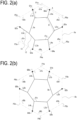
- the virtual pattern Xa is a regular hexagonal pattern that is drawn in a virtual manner on the transparent substrate 11.
- the vertexes of the virtual pattern Xa are a first vertex P1a to a sixth vertex P6a in a counterclockwise direction.
- the intersection point disposed on the side connecting the first vertex P1a and the second vertex P2a is a first intersection point Q1a, and the intersection points disposed on the respective sides of the virtual pattern Xa are a second intersection point Q2a to a sixth intersection point Q6a.
- the first intersection point Q1a to the sixth intersection point Q6a are disposed on the respective sides of the virtual pattern Xa such that the distances between P1a and Q1a, between P1a and Q6a, between P2a and Q2a, between P4a and Q3a, between P4a and Q4a, and between P6a and Q5a are equal.
- Virtual arrows d1a to d6a are respectively drawn below vertexes of the first vertex P1a to the sixth vertex P6a.
- d1a indicates the right direction
- d2a indicates the right obliquely upward direction
- d3a indicates the right obliquely downward direction
- d4a indicates the right direction
- d5a indicates the left obliquely downward direction
- d6a indicates the left obliquely upward direction.
- d2a indicates the right direction
- d3a indicates the left obliquely downward direction
- d4a indicates the right obliquely downward direction
- d5a indicates the left direction
- d6a indicates the right obliquely upward direction
- d1a indicates the right obliquely downward direction.
- a hexagon Sa and connecting lines L1a to L6a are formed by the thin metal wires 12 in the virtual pattern Xa.
- the vertexes of the hexagon Sa and the first intersection point Q1a to the sixth intersection point Q6a are respectively connected by the connecting lines L1a to L6a.
- the hexagon Sa is disposed near the center of the virtual pattern Xa, and the connecting lines L1a to L6a radially extend from vertexes of the hexagon Sa to respective intersection points on sides of the virtual pattern Xa.
- Each of the connecting lines L1a to L6a connects the vertex of the hexagon Sa and either one of the intersection points Q1a to Q6a whose distance from the vertex is shortest.
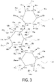
- the inverted virtual pattern Xb is obtained by flipping the virtual pattern Xa horizontally.
- the vertexes of the inverted virtual pattern Xb are a first vertex P1b to a sixth vertex P6b in a clockwise direction.
- the intersection point disposed on the side connecting the first vertex P1b and the second vertex P2b is a first intersection point Q1b, and the intersection points disposed on the respective sides of the inverted virtual pattern Xb are a second intersection point Q2b to a sixth intersection point Q6b.
- the first intersection point Q1b to the sixth intersection point Q6b are disposed on the respective sides of the inverted virtual pattern Xb such that the distances between P1b and Q1b, between P1b and Q6b, between P2b and Q2b, between P4b and Q3b, between P4b and Q4b, and between P6b and Q5b are equal.
- Virtual arrows d1b to d6b are respectively drawn below the vertexes of the first vertex P1b to the sixth vertex P6b.
- d1b indicates the left direction
- d2b indicates the left obliquely upward direction
- d3b indicates the left obliquely downward direction
- d4b indicates the left direction
- d5b indicates the right obliquely downward direction
- d6b indicates the right obliquely upward direction.
- the virtual pattern Xa and the inverted virtual pattern Xb are densely laid such that a number of opening regions formed by the plurality of thin metal wires 12 are aperiodically arranged.
- the virtual pattern Xa and the inverted virtual pattern Xb are densely laid such that the opening regions having the same shape are not periodically arranged.
- the virtual patterns rotated clockwise by 60° are densely laid in combination.
- the virtual patterns to be used are a total of twelve types of the Xa, the Xa rotated by 60°, the Xa rotated by 120°, the Xa rotated by 180°, the virtual pattern Xa rotated by 240°, the Xa rotated by 300°, the Xb, the inverted Xb rotated by 60°, the Xb rotated by 120°, the Xb rotated by 180°, the Xb rotated by 240°, and the Xb rotated by 300°.
- the virtual patterns and the inverted virtual patterns are densely laid such that any one of the intersection points of the virtual pattern or the inverted virtual pattern is overlapped with any one of the intersection points of adjacent virtual pattern or the inverted virtual pattern.
- the connecting line of the virtual pattern or the inverted virtual pattern is always connected to the connecting line of adjacent virtual pattern or the inverted virtual pattern.
- a number of the opening regions R by the plurality of thin metal wires are arranged.
- the opening region R is a polygonal shape formed in the virtual pattern or the inverted virtual pattern, or a region surrounded by the connecting lines and the sides of the polygonal shape.
- the virtual patterns and the inverted virtual patterns are densely laid such that the virtual arrows drawn below the opposed vertexes of the two virtual patterns or the two inverted virtual patterns located opposed via one side of the virtual patterns or the inverted virtual patterns face in the same direction.
- a number of the opening regions formed by the thin metal wires 12 can be aperiodically arranged.
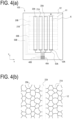
- a virtual pattern X1 is the virtual pattern Xa in FIG. 2(a)
- a virtual pattern X2 is obtained by rotating the inverted virtual pattern Xb in FIG. 2(b) clockwise by 240°
- a virtual pattern X3 is obtained by rotating the Xa clockwise by 240°.
- the X1 and X2 are located adjacent such that the side P3a-P4a of the X1 and the side P3b-P4b of the X2 are overlapped. In other words, the X1 and X2 share the side P3a-P4a of the X1 (or the side P3b-P4b of the X2).
- the X2 and X3 are located adjacent such that the side P5b-P6b of the X2 and the side P5a-P6a of the X3 are overlapped. In other words, the x2 and X3 share the side P5b-P6b of the X2 (or the side P5a-P6a of the X3).
- the X1 and X3 are located opposed to each other via the side P4b-P5b of the X2.
- the X1 and X3 are disposed such that the vertex P4a of the X1 and the vertex P5a of the X3 are located opposed to each other.
- a connecting line L5b of the X2 and a connecting line L5a of the X3 are connected.
- the X1 and X3 are located opposed to each other via the side P4b-P5b of the X2, and are arranged such that the fourth vertex P4a of the X1 and the fifth vertex P5a of the X2 are located opposed to each other.
- P1a is on the upper side and P4a is on the lower side as the line connecting P1a
- P4a of the X1 is defined as the axis
- the directions indicated by the virtual arrow d4a of the fourth vertex P4a of the X1 and the virtual arrow d5a of the fifth vertex P5a of the X3 are both arrows that indicate the right direction.
- a number of the opening regions formed by the thin metal wires are aperiodically arranged.
- a length A of one side of the virtual pattern Xa is 150 ⁇ m to 3000 ⁇ m, and is preferably 500 ⁇ m to 2000 ⁇ m.
- the length is 150 ⁇ m or more, the thin metal wires 12 can be prevented from being densely formed on the transparent substrate.
- the length is 3000 ⁇ m or less, the number of thin metal wires 12 is reduced, and the resistance value can be prevented from increasing.
- a length B of one side of the hexagon Sa is preferably from A/4 ⁇ m to 3A/4 ⁇ m.
- the hexagon Sa can be prevented from having the area extremely different from that of the graphic formed by the connecting lines and the sides of the hexagon, and a location where the thin metal wires are sparsely disposed and a location where the thin metal wires are closely disposed can be prevented from being formed.
- Each inner angle ⁇ of the hexagon Sa is preferably 90° or greater. When the inner angle ⁇ is 90° or greater, the thin metal wires are controlled to have the equal width near intersection points of the thin metal wires, and the increase of the width of the thin metal wires near the vertex of the hexagon Sa can be prevented from causing glare.
- a length C of each of the connecting lines L1a to L6a is preferably A/4 ⁇ m to A/2 ⁇ m.
- the hexagon Sa can be prevented from having the area extremely different from that of the graphic formed by the connecting lines and the sides of the hexagon Sa, and a location where the thin metal wires are sparsely disposed and a location where the thin metal wires are closely disposed can be prevented from being formed.
- the conductive sheet 10 can be manufactured by a method in which a metal film including a blackened layer is formed on the transparent substrate 11 by sputtering or transferring metal foil to be patterned by etching, or a method in which conductive ink is pattern-printed on the transparent substrate 11.
- the hexagon Sa and the connecting lines L1a to L6a are formed by the thin metal wires 12 in the virtual pattern Xa, and the vertexes of the hexagon Sa and the first intersection point Q1a to the sixth intersection point Q6a are respectively connected by the connecting lines L1a to L6a.
- the thin metal wires 12 can be prevented from being densely disposed, or the resistance value can be prevented from being increased by a decreased number of thin metal wires 12.
- the length B of one side of the hexagon Sa is A/4 ⁇ B ⁇ 3A/4, and each of the connecting lines L1a to L6a connects the vertex of the hexagon Sa and the intersection point located at the shortest distance from the vertex.
- the hexagon Sa is disposed near the center of the virtual pattern Xa, and the connecting lines L1a to L6a are disposed to radially extend from vertexes of the hexagon Sa to respective sides of the virtual pattern Xa.
- a touch sensor 100 includes the transparent substrate 11, a plurality of electrodes 20A formed on one surface of the transparent substrate 11, connection portions 30A each formed on an end portion of the plurality of electrodes 20A, terminal portions 40A connected to external wiring lines, and routed wiring lines 50A each connecting the connection portion 30A and the terminal portion 40A. Further, the touch sensor 100 includes a plurality of electrodes 20B formed on the other surface of the transparent substrate 11, connection portions 30B each formed on an end portion of the plurality of electrodes 20B, terminal portions 40B connected to the external wiring lines, and routed wiring lines 50B each connecting the connection portion 30B and the terminal portion 40B.
- the transparent substrate 11 is sectioned into an operation region V1 and a peripheral region V2.
- the operation region V1 is a region of the touch sensor 100 in which an input operation by a user is performed
- the peripheral region V2 is a region that is covered by a frame-shaped decorative layer or the like of a cover base material after assembly.
- the plurality of electrodes 20A and dummy portions 21A are formed in the operation region V1 on one surface of the transparent substrate, and the connection portions 30A, the terminal portions 40A, and the routed wiring lines 50A are formed in the peripheral region V2.
- the plurality of electrodes 20A are formed in the operation region V1.
- the plurality of electrodes 20A have a band shape, and are arranged on the top surface of the transparent substrate 11 to extend in the y-axis direction and be located side by side in four rows in the x-axis direction.
- the plurality of electrodes 20A is made up of the plurality of thin metal wires described in the first embodiment.
- the plurality of electrodes 20A form electrodes of the touch sensor.
- the size of the plurality of electrodes 20A is determined by the size of the operation region V1 and resolution and thus is not limited to particular sizes, and when the length of one side of the virtual pattern Xa described above is A and the width of the electrode 20A is W, the relationship 3A ⁇ W is preferably satisfied.
- the dummy portion 21A is formed in a region of the operation region V1 in which the plurality of electrodes 20A are not formed.
- the electrodes 20A and the dummy portions 21A are alternately arranged.
- the dummy portions 21A are made up of the plurality of thin metal wires described in the first embodiment. Referring to FIG. 4 (b) , when a region K including the boundary of the electrode 20A and the dummy portion 21A in FIG. 4A is enlarged, the electrode 20A and the dummy portion 21A are disconnected by a disconnection portion 22A so as not to be electrically connected.
- the disconnection portion 22A is formed to section the operation region V1 and form the band shape of the electrode 20A, and the electrode 20A and the dummy portion are separated by the disconnection portion 22A.
- the thin metal wire 12 is not formed in the disconnection portion 22A.
- the width of the disconnection portion 22A is preferably 1 to 10 ⁇ m. When the width of the disconnection portion 22A is in such a range, the appearance of the boundary line between the electrode and the dummy portion due to the presence or absence of the thin metal wire can be prevented.
- connection portion 30A serves to connect the electrode 20A and the routed wiring line 40A.
- the thin metal wires 12 forming the electrode 20A can be collectively connected by the connection portion 30A to the routed wiring line 40A.
- the connection portion 30A has a rectangular shape and is formed at one end in the longitudinal direction of the electrode 20A having a band shape.
- the connection portions 30A are formed in the peripheral region V2 to be partially overlapped with the plurality of thin metal wires 12 forming the plurality of electrodes 20A.
- the electrode 20A extends to the boundary line of the operation region V1, and one side of the rectangular shape of the connection portion 30A is overlapped with the boundary line between the operation region V1 and the peripheral region V2.
- the width of the connection portion 30A is equal to the width of the electrode 20A.
- the connection portion 30A is formed of a layered film of the first blackened layer, the metal layer, and the second blackened layer that are layered in the mentioned order from the transparent substrate 11 side.
- the terminal portion 40A serves to connect the touch sensor 100 to an external wiring line of a flexible wiring substrate or the like, and is formed near an outer edge on the transparent substrate 11.
- the routed wiring line 50A serves to connect the electrode 20A and the terminal portion 40A, and the routed wiring lines 50A are connected to the terminal portions 40A to be bent in the middle and gathered near the center.
- the terminal portion 40A and the routed wiring line 50A are each formed of the first blackened layer, the metal layer, and the second blackened layer that are layered in the mentioned order from the transparent substrate 11 side.
- the plurality of electrodes 20B and dummy portions 21B are formed in the operation region V1 on the other surface of the transparent substrate, and the connection portions 30B and the terminal portions 40B are formed in the peripheral region V2.
- the plurality of electrodes 20B are disposed on the back surface of the transparent substrate 11 to extend in the x-axis direction and be located side by side in five rows in the y-axis direction.
- the connection portion 30B is formed at one end in the longitudinal direction of each of the plurality of electrodes 20B having a band shape.
- the terminal portions 40A and 40B formed on the top surface and back surface of the transparent substrate 11 are connected to a flexible printed circuit board (not illustrated).
- the flexible printed circuit board is connected to a control unit that achieves capacitive touch detection.
- the control unit detects a current flowing in response to changes in electrostatic capacitance, which occur in the plurality of electrodes 20A and 20B when the finger of a user or a conducting body of a stylus or the like is closely located or separated, and thus a touch operation and a touch position by the user can be detected.
- a method for manufacturing the touch sensor 100 will be described.
- a first blackened film layer, a metal film layer, and a second blackened film layer are formed in the mentioned order on the both surfaces of the transparent substrate 11 by sputtering or transferring metal foil. Additionally, a resist layer is formed on the second blackened film layer, and the resist layer is patterned by exposure and developing with a pattern mask. Thereafter, by etching the first blackened film layer, the metal film layer, and the second blackened film layer with the patterned resist layer used as an etching mask, electrodes formed of a plurality of thin metal wires, dummy portions, disconnection portions, connection portions, terminal portions, and routed wiring lines are simultaneously formed on the both surfaces of the transparent substrate 11.
- the plurality of electrodes 20A and 20B are formed of the plurality of thin metal wires according to the first embodiment, and thus the occurrence of glare due to a difference between a location where the thin metal wires are sparsely disposed and a location where the thin metal wires are closely disposed or glare due to the increase of the width of the thin metal wires near the intersection points at which the thin metal wires intersect one another can be suppressed.
- the dummy portions are formed in locations in the operation region V1 in which the plurality of electrodes are not formed, the phenomenon where the shape of the electrode pattern is observed by an operator due to the presence or absence of electrodes can be suppressed, and thus deterioration in visibility can be prevented.
- the dummy portions are formed of the plurality of thin metal wires according to the first embodiment in the same manner as the plurality of electrodes, the occurrence of glare can be suppressed in both the dummy portions and the plurality of electrodes. As a result, the visibility of the operation region V1 of the touch sensor 100 can be improved.
- the plurality of electrodes, the dummy portions, the connection portions, the terminal portions, and the routed wiring lines can be simultaneously formed, and thus the manufacturing process can be prevented from being complicated.
- the hexagon Sa is formed in the virtual pattern Xa, but Sa may be an n-sided polygon (n ⁇ 5).
- n 5 that is, Sa is a pentagon
- five connecting lines of the connecting lines L1a to L6a connect the vertexes of the pentagon Sa and the intersection points on the virtual pattern Xa
- the remaining one connecting line connects the side of the pentagon Sa and the remaining intersection point on the virtual pattern Xa.
- the length C of each of the connecting lines L1a to L6a is preferably in the range A/4 ⁇ C ⁇ A/2.
- the connecting lines L1a to L6a may connect the vertexes of the polygon Sa and the intersection points on the virtual pattern Xa, which are located at the shortest distance from the vertexes. Additionally, the length C of each of the connecting lines L1a to L6a may be in the range A/4 ⁇ C ⁇ A/2.
- the virtual pattern Xa and the inverted virtual pattern Xb that are rotated clockwise are used and densely laid; however, the virtual pattern Xa and the inverted virtual pattern Xb may be rotated counterclockwise and used.
- the opening region is formed only by the polygon and the connecting lines that are formed in the virtual pattern Xa and the inverted virtual pattern Xb, and thus the thin metal wires 12 are formed in a mesh shape; however, the thin metal wires 12 may be further added. In this case, the thin metal wires 12 are disposed such that the added thin metal wires 12 are not periodically arranged.
- the thin metal wire 12 is formed of the first blackened layer, the metal layer, and the second blackened layer that are layered in the mentioned order; however, the layered configuration of the thin metal wire is not limited thereto.
- the thin metal wire may include only a metal layer, may include a metal layer and a blackened layer that are layered in this order from the transparent substrate side, or may include a blackened layer formed to cover the upper surface and side surfaces of a metal layer formed on the transparent substrate.
- the periphery of a metal layer may be completely covered by a blackened layer. In such a configuration, glare when the touch sensor is assembled can be further suppressed.
- the plurality of thin metal wires are formed on one surface of the transparent substrate of the conductive sheet; however, the thin metal wires may be formed on the both surfaces of the transparent substrate. In this case, when blackened layers are formed on at least the upper and lower surfaces of a metal layer, visibility can be further improved.
- the plurality of electrodes 20A and 20B have a belt shape; however, the shape of the electrode is not limited thereto.
- Another shape of the electrode can be, for example, a shape in which rhombuses are continuously disposed or a comb teeth shape.
- the number of electrodes, the position of the routed wiring lines, and the position of the terminal portions are not particularly limited.
- the dummy portion is formed of the thin metal wires according to the first embodiment; however, the thin metal wire pattern of the dummy portion is not limited thereto.
- the dummy portion may be formed of a thin metal wire pattern that can suppress the occurrence of glare.
- the electrodes are formed on the both surfaces of the transparent substrate 11 of the touch sensor 100; however, the configuration of the touch sensor is not limited thereto.
- Two transparent substrates each having electrodes formed on one surface thereof may be attached such that the other surfaces of the transparent substrates are located opposed to each other or that the other surface of the transparent substrate may be adhered in an overlapping manner to the electrodes via an adhesive thereon.
- connection portion is formed at one end of the electrode; however, the connection portions may be formed at both ends in the longitudinal direction of the electrode.
- connection portion 30B is formed at the left end portion of the electrode 20B, and in the meantime, the connection portion 30B may be further formed at the right end portion of the electrode 20B.
- the terminal portions 40B are also formed on the right side of the terminal portions 40A, and the routed wiring lines 50B are connected to the respective terminal portions 40B.
- the position of the terminal portions and the arrangement of the routed wiring lines are not limited to particular positions.
- the plurality of electrodes, the dummy portions, the connection portions, the terminal portions, and the routed wiring lines are simultaneously formed; however, the method for manufacturing the touch sensor 100 is not limited thereto.
- the thin metal wires according to the first embodiment are formed in the operation region V1; thereafter, the disconnection portions are formed by cutting the thin metal wires with a laser, and the plurality of electrodes and the dummy portions may be formed.
- the plurality of electrodes and the dummy portions are formed in the operation region V1; thereafter, the connection portions, the terminal portions, and the routed wiring lines may be formed in the peripheral region V2.
- the portions instead of simultaneously forming the portions on the both surfaces of the transparent substrate 11, the portions may be separately formed on each one of the surfaces.
Landscapes
- Engineering & Computer Science (AREA)
- General Engineering & Computer Science (AREA)
- Theoretical Computer Science (AREA)
- Human Computer Interaction (AREA)
- Physics & Mathematics (AREA)
- General Physics & Mathematics (AREA)
- Position Input By Displaying (AREA)
Applications Claiming Priority (2)
| Application Number | Priority Date | Filing Date | Title |
|---|---|---|---|
| JP2020089388A JP7012120B2 (ja) | 2020-05-22 | 2020-05-22 | 導電シート、タッチセンサ及びタッチセンサの製造方法 |
| PCT/JP2021/015625 WO2021235145A1 (ja) | 2020-05-22 | 2021-04-15 | 導電シート、タッチセンサ及びタッチセンサの製造方法 |
Publications (3)
| Publication Number | Publication Date |
|---|---|
| EP4137920A1 true EP4137920A1 (de) | 2023-02-22 |
| EP4137920A4 EP4137920A4 (de) | 2023-09-20 |
| EP4137920B1 EP4137920B1 (de) | 2024-05-01 |
Family
ID=78708917
Family Applications (1)
| Application Number | Title | Priority Date | Filing Date |
|---|---|---|---|
| EP21807696.6A Active EP4137920B1 (de) | 2020-05-22 | 2021-04-15 | Leitfähige folie, berührungssensor und verfahren zur herstellung eines berührungssensors |
Country Status (7)
| Country | Link |
|---|---|
| US (1) | US11868157B2 (de) |
| EP (1) | EP4137920B1 (de) |
| JP (1) | JP7012120B2 (de) |
| KR (1) | KR102838884B1 (de) |
| CN (1) | CN115698920B (de) |
| TW (1) | TWI865771B (de) |
| WO (1) | WO2021235145A1 (de) |
Families Citing this family (3)
| Publication number | Priority date | Publication date | Assignee | Title |
|---|---|---|---|---|
| US12210714B2 (en) * | 2022-12-22 | 2025-01-28 | Tpk Advanced Solutions Inc. | Touch module and method of manufacturing the same |
| CN116518845B (zh) * | 2023-05-09 | 2025-09-26 | 杭州电子科技大学 | 一种足球式结构的球铰关节转动角度测量装置及方法 |
| CN121832795A (zh) * | 2024-10-08 | 2026-04-10 | 合肥鑫晟光电科技有限公司 | 金属网格、触控基板和触控显示装置 |
Family Cites Families (21)
| Publication number | Priority date | Publication date | Assignee | Title |
|---|---|---|---|---|
| CN102308366B (zh) * | 2009-02-06 | 2015-08-12 | Lg化学株式会社 | 触摸屏及其制备方法 |
| EP2401669B1 (de) | 2009-02-26 | 2016-04-06 | 3M Innovative Properties Company | Berührungsschirmsensor und strukturiertes substrat mit überlagerten mikrostrukturen mit geringer sichtbarkeit |
| WO2011125597A1 (ja) * | 2010-03-31 | 2011-10-13 | 富士フイルム株式会社 | 導電性フイルムの製造方法、導電性フイルム及び記録媒体 |
| JP5781886B2 (ja) * | 2011-10-05 | 2015-09-24 | 富士フイルム株式会社 | 導電シート、タッチパネル及び表示装置 |
| JP5224203B1 (ja) * | 2012-07-11 | 2013-07-03 | 大日本印刷株式会社 | タッチパネルセンサ、タッチパネル装置および表示装置 |
| KR20140025922A (ko) | 2012-08-23 | 2014-03-05 | 삼성전기주식회사 | 터치패널 |
| JP2014191445A (ja) * | 2013-03-26 | 2014-10-06 | Fujifilm Corp | タッチパネル及び表示装置 |
| JP6127666B2 (ja) | 2013-04-04 | 2017-05-17 | 大日本印刷株式会社 | 導電性メッシュ、導電性メッシュシート、タッチパネル装置および画像表示装置 |
| KR102108846B1 (ko) * | 2013-07-16 | 2020-05-11 | 엘지이노텍 주식회사 | 터치 윈도우 |
| WO2015030090A1 (ja) * | 2013-08-30 | 2015-03-05 | 富士フイルム株式会社 | 導電性フィルム、それを備えるタッチパネル及び表示装置、並びに導電性フィルムの評価方法 |
| JP6195157B2 (ja) | 2013-10-01 | 2017-09-13 | 大日本印刷株式会社 | 導電性メッシュ、導電性メッシュシート、タッチパネル装置および画像表示装置 |
| JP6156742B2 (ja) | 2013-10-01 | 2017-07-05 | 大日本印刷株式会社 | 導電性メッシュ、導電性メッシュシート、タッチパネル装置および画像表示装置 |
| CN104571673A (zh) * | 2013-10-18 | 2015-04-29 | 胜华科技股份有限公司 | 触控面板 |
| JP6294506B2 (ja) | 2014-11-21 | 2018-03-14 | 富士フイルム株式会社 | 導電性フィルム、及びこれを備えるタッチパネルセンサ、並びに、タッチパネルセンサ |
| JP6445365B2 (ja) | 2015-03-26 | 2018-12-26 | 大日本印刷株式会社 | 透視性電極、該透視性電極を用いてなるタッチパネル用位置検知電極、タッチパネル、及び画像表示装置 |
| KR102160020B1 (ko) * | 2015-07-24 | 2020-09-25 | 후지필름 가부시키가이샤 | 터치 패널용 도전 필름, 터치 패널, 및 터치 패널 부착 표시 장치 |
| WO2017018051A1 (ja) * | 2015-07-24 | 2017-02-02 | 富士フイルム株式会社 | タッチパネル用導電フィルムのメッシュパターン設計方法、タッチパネル用導電フィルムの製造方法およびタッチパネル用導電フィルム |
| WO2017086216A1 (ja) * | 2015-11-17 | 2017-05-26 | 三菱製紙株式会社 | 光透過性導電材料 |
| CN106990858A (zh) * | 2016-01-21 | 2017-07-28 | 倍胜光电股份有限公司 | 可消除莫瑞效应的触控面板 |
| JP2019179462A (ja) | 2018-03-30 | 2019-10-17 | 三菱製紙株式会社 | 光透過性導電材料 |
| CN208000558U (zh) * | 2018-04-25 | 2018-10-23 | 信利光电股份有限公司 | 一种触控面板及电子装置 |
-
2020
- 2020-05-22 JP JP2020089388A patent/JP7012120B2/ja active Active
-
2021
- 2021-04-15 US US17/926,575 patent/US11868157B2/en active Active
- 2021-04-15 KR KR1020227037897A patent/KR102838884B1/ko active Active
- 2021-04-15 CN CN202180036909.0A patent/CN115698920B/zh active Active
- 2021-04-15 WO PCT/JP2021/015625 patent/WO2021235145A1/ja not_active Ceased
- 2021-04-15 EP EP21807696.6A patent/EP4137920B1/de active Active
- 2021-04-21 TW TW110114317A patent/TWI865771B/zh active
Also Published As
| Publication number | Publication date |
|---|---|
| EP4137920A4 (de) | 2023-09-20 |
| KR20230014683A (ko) | 2023-01-30 |
| JP7012120B2 (ja) | 2022-01-27 |
| CN115698920B (zh) | 2025-07-01 |
| TW202204847A (zh) | 2022-02-01 |
| WO2021235145A1 (ja) | 2021-11-25 |
| US20230205378A1 (en) | 2023-06-29 |
| JP2021184175A (ja) | 2021-12-02 |
| CN115698920A (zh) | 2023-02-03 |
| KR102838884B1 (ko) | 2025-07-25 |
| TWI865771B (zh) | 2024-12-11 |
| EP4137920B1 (de) | 2024-05-01 |
| US11868157B2 (en) | 2024-01-09 |
Similar Documents
| Publication | Publication Date | Title |
|---|---|---|
| CN107111394B (zh) | 导电性薄膜及具备该导电性薄膜的触摸面板传感器 | |
| EP4137920A1 (de) | Leitfähige folie, berührungssensor und verfahren zur herstellung eines berührungssensors | |
| US10282007B2 (en) | Display device | |
| TWI796372B (zh) | 導電構件及觸控面板 | |
| JP5795038B2 (ja) | 静電容量方式タッチパネル用電極シート | |
| US20170031490A1 (en) | Touch sensor electrode, touch panel and display device | |
| CN114679912B (zh) | 触控面板及触控显示装置 | |
| JP2020532776A (ja) | タッチ基板及びその製造方法、表示パネル | |
| CN113467650B (zh) | 触控显示面板及显示装置 | |
| WO2013111795A1 (ja) | 透明導電性素子、入力装置、電子機器および透明導電性素子作製用原盤 | |
| KR20120111985A (ko) | 입력 장치 및 그 제조 방법 | |
| CN108021288A (zh) | 一种触控面板及其制作方法、显示装置 | |
| CN105278786B (zh) | 触摸板 | |
| US20140340592A1 (en) | Touch panel and method of fabricating the same | |
| US20240201815A1 (en) | Conductive sheet, touch sensor, and method for manufacturing touch sensor | |
| TW202238349A (zh) | 靜電電容式觸碰面板 | |
| JP7356578B2 (ja) | 静電容量式センサおよび入力装置 | |
| JP2025000189A (ja) | 導電フィルム | |
| KR101370402B1 (ko) | 터치패널의 전극형성방법 및 이를 이용한 터치패널의 전극구조 | |
| CN103713757A (zh) | 触控板 |
Legal Events
| Date | Code | Title | Description |
|---|---|---|---|
| STAA | Information on the status of an ep patent application or granted ep patent |
Free format text: STATUS: THE INTERNATIONAL PUBLICATION HAS BEEN MADE |
|
| PUAI | Public reference made under article 153(3) epc to a published international application that has entered the european phase |
Free format text: ORIGINAL CODE: 0009012 |
|
| STAA | Information on the status of an ep patent application or granted ep patent |
Free format text: STATUS: REQUEST FOR EXAMINATION WAS MADE |
|
| 17P | Request for examination filed |
Effective date: 20221117 |
|
| AK | Designated contracting states |
Kind code of ref document: A1 Designated state(s): AL AT BE BG CH CY CZ DE DK EE ES FI FR GB GR HR HU IE IS IT LI LT LU LV MC MK MT NL NO PL PT RO RS SE SI SK SM TR |
|
| DAV | Request for validation of the european patent (deleted) | ||
| DAX | Request for extension of the european patent (deleted) | ||
| A4 | Supplementary search report drawn up and despatched |
Effective date: 20230821 |
|
| RIC1 | Information provided on ipc code assigned before grant |
Ipc: G06F 3/044 20060101ALI20230814BHEP Ipc: G06F 3/041 20060101AFI20230814BHEP |
|
| GRAP | Despatch of communication of intention to grant a patent |
Free format text: ORIGINAL CODE: EPIDOSNIGR1 |
|
| STAA | Information on the status of an ep patent application or granted ep patent |
Free format text: STATUS: GRANT OF PATENT IS INTENDED |
|
| INTG | Intention to grant announced |
Effective date: 20240110 |
|
| GRAS | Grant fee paid |
Free format text: ORIGINAL CODE: EPIDOSNIGR3 |
|
| GRAA | (expected) grant |
Free format text: ORIGINAL CODE: 0009210 |
|
| STAA | Information on the status of an ep patent application or granted ep patent |
Free format text: STATUS: THE PATENT HAS BEEN GRANTED |
|
| AK | Designated contracting states |
Kind code of ref document: B1 Designated state(s): AL AT BE BG CH CY CZ DE DK EE ES FI FR GB GR HR HU IE IS IT LI LT LU LV MC MK MT NL NO PL PT RO RS SE SI SK SM TR |
|
| REG | Reference to a national code |
Ref country code: GB Ref legal event code: FG4D |
|
| REG | Reference to a national code |
Ref country code: CH Ref legal event code: EP |
|
| REG | Reference to a national code |
Ref country code: DE Ref legal event code: R096 Ref document number: 602021012851 Country of ref document: DE |
|
| REG | Reference to a national code |
Ref country code: IE Ref legal event code: FG4D |
|
| REG | Reference to a national code |
Ref country code: LT Ref legal event code: MG9D |
|
| REG | Reference to a national code |
Ref country code: NL Ref legal event code: MP Effective date: 20240501 |
|
| PG25 | Lapsed in a contracting state [announced via postgrant information from national office to epo] |
Ref country code: IS Free format text: LAPSE BECAUSE OF FAILURE TO SUBMIT A TRANSLATION OF THE DESCRIPTION OR TO PAY THE FEE WITHIN THE PRESCRIBED TIME-LIMIT Effective date: 20240901 |
|
| PG25 | Lapsed in a contracting state [announced via postgrant information from national office to epo] |
Ref country code: BG Free format text: LAPSE BECAUSE OF FAILURE TO SUBMIT A TRANSLATION OF THE DESCRIPTION OR TO PAY THE FEE WITHIN THE PRESCRIBED TIME-LIMIT Effective date: 20240501 |
|
| PG25 | Lapsed in a contracting state [announced via postgrant information from national office to epo] |
Ref country code: HR Free format text: LAPSE BECAUSE OF FAILURE TO SUBMIT A TRANSLATION OF THE DESCRIPTION OR TO PAY THE FEE WITHIN THE PRESCRIBED TIME-LIMIT Effective date: 20240501 Ref country code: FI Free format text: LAPSE BECAUSE OF FAILURE TO SUBMIT A TRANSLATION OF THE DESCRIPTION OR TO PAY THE FEE WITHIN THE PRESCRIBED TIME-LIMIT Effective date: 20240501 |
|
| PG25 | Lapsed in a contracting state [announced via postgrant information from national office to epo] |
Ref country code: GR Free format text: LAPSE BECAUSE OF FAILURE TO SUBMIT A TRANSLATION OF THE DESCRIPTION OR TO PAY THE FEE WITHIN THE PRESCRIBED TIME-LIMIT Effective date: 20240802 |
|
| PG25 | Lapsed in a contracting state [announced via postgrant information from national office to epo] |
Ref country code: PT Free format text: LAPSE BECAUSE OF FAILURE TO SUBMIT A TRANSLATION OF THE DESCRIPTION OR TO PAY THE FEE WITHIN THE PRESCRIBED TIME-LIMIT Effective date: 20240902 |
|
| REG | Reference to a national code |
Ref country code: AT Ref legal event code: MK05 Ref document number: 1683263 Country of ref document: AT Kind code of ref document: T Effective date: 20240501 |
|
| PG25 | Lapsed in a contracting state [announced via postgrant information from national office to epo] |
Ref country code: NL Free format text: LAPSE BECAUSE OF FAILURE TO SUBMIT A TRANSLATION OF THE DESCRIPTION OR TO PAY THE FEE WITHIN THE PRESCRIBED TIME-LIMIT Effective date: 20240501 |
|
| PG25 | Lapsed in a contracting state [announced via postgrant information from national office to epo] |
Ref country code: ES Free format text: LAPSE BECAUSE OF FAILURE TO SUBMIT A TRANSLATION OF THE DESCRIPTION OR TO PAY THE FEE WITHIN THE PRESCRIBED TIME-LIMIT Effective date: 20240501 |
|
| PG25 | Lapsed in a contracting state [announced via postgrant information from national office to epo] |
Ref country code: AT Free format text: LAPSE BECAUSE OF FAILURE TO SUBMIT A TRANSLATION OF THE DESCRIPTION OR TO PAY THE FEE WITHIN THE PRESCRIBED TIME-LIMIT Effective date: 20240501 |
|
| PG25 | Lapsed in a contracting state [announced via postgrant information from national office to epo] |
Ref country code: PL Free format text: LAPSE BECAUSE OF FAILURE TO SUBMIT A TRANSLATION OF THE DESCRIPTION OR TO PAY THE FEE WITHIN THE PRESCRIBED TIME-LIMIT Effective date: 20240501 |
|
| PG25 | Lapsed in a contracting state [announced via postgrant information from national office to epo] |
Ref country code: LV Free format text: LAPSE BECAUSE OF FAILURE TO SUBMIT A TRANSLATION OF THE DESCRIPTION OR TO PAY THE FEE WITHIN THE PRESCRIBED TIME-LIMIT Effective date: 20240501 |
|
| PG25 | Lapsed in a contracting state [announced via postgrant information from national office to epo] |
Ref country code: PT Free format text: LAPSE BECAUSE OF FAILURE TO SUBMIT A TRANSLATION OF THE DESCRIPTION OR TO PAY THE FEE WITHIN THE PRESCRIBED TIME-LIMIT Effective date: 20240902 Ref country code: PL Free format text: LAPSE BECAUSE OF FAILURE TO SUBMIT A TRANSLATION OF THE DESCRIPTION OR TO PAY THE FEE WITHIN THE PRESCRIBED TIME-LIMIT Effective date: 20240501 Ref country code: NO Free format text: LAPSE BECAUSE OF FAILURE TO SUBMIT A TRANSLATION OF THE DESCRIPTION OR TO PAY THE FEE WITHIN THE PRESCRIBED TIME-LIMIT Effective date: 20240801 Ref country code: NL Free format text: LAPSE BECAUSE OF FAILURE TO SUBMIT A TRANSLATION OF THE DESCRIPTION OR TO PAY THE FEE WITHIN THE PRESCRIBED TIME-LIMIT Effective date: 20240501 Ref country code: LV Free format text: LAPSE BECAUSE OF FAILURE TO SUBMIT A TRANSLATION OF THE DESCRIPTION OR TO PAY THE FEE WITHIN THE PRESCRIBED TIME-LIMIT Effective date: 20240501 Ref country code: IS Free format text: LAPSE BECAUSE OF FAILURE TO SUBMIT A TRANSLATION OF THE DESCRIPTION OR TO PAY THE FEE WITHIN THE PRESCRIBED TIME-LIMIT Effective date: 20240901 Ref country code: HR Free format text: LAPSE BECAUSE OF FAILURE TO SUBMIT A TRANSLATION OF THE DESCRIPTION OR TO PAY THE FEE WITHIN THE PRESCRIBED TIME-LIMIT Effective date: 20240501 Ref country code: GR Free format text: LAPSE BECAUSE OF FAILURE TO SUBMIT A TRANSLATION OF THE DESCRIPTION OR TO PAY THE FEE WITHIN THE PRESCRIBED TIME-LIMIT Effective date: 20240802 Ref country code: FI Free format text: LAPSE BECAUSE OF FAILURE TO SUBMIT A TRANSLATION OF THE DESCRIPTION OR TO PAY THE FEE WITHIN THE PRESCRIBED TIME-LIMIT Effective date: 20240501 Ref country code: ES Free format text: LAPSE BECAUSE OF FAILURE TO SUBMIT A TRANSLATION OF THE DESCRIPTION OR TO PAY THE FEE WITHIN THE PRESCRIBED TIME-LIMIT Effective date: 20240501 Ref country code: BG Free format text: LAPSE BECAUSE OF FAILURE TO SUBMIT A TRANSLATION OF THE DESCRIPTION OR TO PAY THE FEE WITHIN THE PRESCRIBED TIME-LIMIT Effective date: 20240501 Ref country code: AT Free format text: LAPSE BECAUSE OF FAILURE TO SUBMIT A TRANSLATION OF THE DESCRIPTION OR TO PAY THE FEE WITHIN THE PRESCRIBED TIME-LIMIT Effective date: 20240501 Ref country code: RS Free format text: LAPSE BECAUSE OF FAILURE TO SUBMIT A TRANSLATION OF THE DESCRIPTION OR TO PAY THE FEE WITHIN THE PRESCRIBED TIME-LIMIT Effective date: 20240801 |
|
| PG25 | Lapsed in a contracting state [announced via postgrant information from national office to epo] |
Ref country code: DK Free format text: LAPSE BECAUSE OF FAILURE TO SUBMIT A TRANSLATION OF THE DESCRIPTION OR TO PAY THE FEE WITHIN THE PRESCRIBED TIME-LIMIT Effective date: 20240501 |
|
| PG25 | Lapsed in a contracting state [announced via postgrant information from national office to epo] |
Ref country code: EE Free format text: LAPSE BECAUSE OF FAILURE TO SUBMIT A TRANSLATION OF THE DESCRIPTION OR TO PAY THE FEE WITHIN THE PRESCRIBED TIME-LIMIT Effective date: 20240501 |
|
| PG25 | Lapsed in a contracting state [announced via postgrant information from national office to epo] |
Ref country code: CZ Free format text: LAPSE BECAUSE OF FAILURE TO SUBMIT A TRANSLATION OF THE DESCRIPTION OR TO PAY THE FEE WITHIN THE PRESCRIBED TIME-LIMIT Effective date: 20240501 |
|
| PG25 | Lapsed in a contracting state [announced via postgrant information from national office to epo] |
Ref country code: SK Free format text: LAPSE BECAUSE OF FAILURE TO SUBMIT A TRANSLATION OF THE DESCRIPTION OR TO PAY THE FEE WITHIN THE PRESCRIBED TIME-LIMIT Effective date: 20240501 Ref country code: RO Free format text: LAPSE BECAUSE OF FAILURE TO SUBMIT A TRANSLATION OF THE DESCRIPTION OR TO PAY THE FEE WITHIN THE PRESCRIBED TIME-LIMIT Effective date: 20240501 |
|
| PG25 | Lapsed in a contracting state [announced via postgrant information from national office to epo] |
Ref country code: SM Free format text: LAPSE BECAUSE OF FAILURE TO SUBMIT A TRANSLATION OF THE DESCRIPTION OR TO PAY THE FEE WITHIN THE PRESCRIBED TIME-LIMIT Effective date: 20240501 |
|
| PG25 | Lapsed in a contracting state [announced via postgrant information from national office to epo] |
Ref country code: SM Free format text: LAPSE BECAUSE OF FAILURE TO SUBMIT A TRANSLATION OF THE DESCRIPTION OR TO PAY THE FEE WITHIN THE PRESCRIBED TIME-LIMIT Effective date: 20240501 Ref country code: SK Free format text: LAPSE BECAUSE OF FAILURE TO SUBMIT A TRANSLATION OF THE DESCRIPTION OR TO PAY THE FEE WITHIN THE PRESCRIBED TIME-LIMIT Effective date: 20240501 Ref country code: RO Free format text: LAPSE BECAUSE OF FAILURE TO SUBMIT A TRANSLATION OF THE DESCRIPTION OR TO PAY THE FEE WITHIN THE PRESCRIBED TIME-LIMIT Effective date: 20240501 Ref country code: EE Free format text: LAPSE BECAUSE OF FAILURE TO SUBMIT A TRANSLATION OF THE DESCRIPTION OR TO PAY THE FEE WITHIN THE PRESCRIBED TIME-LIMIT Effective date: 20240501 Ref country code: DK Free format text: LAPSE BECAUSE OF FAILURE TO SUBMIT A TRANSLATION OF THE DESCRIPTION OR TO PAY THE FEE WITHIN THE PRESCRIBED TIME-LIMIT Effective date: 20240501 Ref country code: CZ Free format text: LAPSE BECAUSE OF FAILURE TO SUBMIT A TRANSLATION OF THE DESCRIPTION OR TO PAY THE FEE WITHIN THE PRESCRIBED TIME-LIMIT Effective date: 20240501 |
|
| REG | Reference to a national code |
Ref country code: DE Ref legal event code: R097 Ref document number: 602021012851 Country of ref document: DE |
|
| PG25 | Lapsed in a contracting state [announced via postgrant information from national office to epo] |
Ref country code: IT Free format text: LAPSE BECAUSE OF FAILURE TO SUBMIT A TRANSLATION OF THE DESCRIPTION OR TO PAY THE FEE WITHIN THE PRESCRIBED TIME-LIMIT Effective date: 20240501 |
|
| PLBE | No opposition filed within time limit |
Free format text: ORIGINAL CODE: 0009261 |
|
| STAA | Information on the status of an ep patent application or granted ep patent |
Free format text: STATUS: NO OPPOSITION FILED WITHIN TIME LIMIT |
|
| 26N | No opposition filed |
Effective date: 20250204 |
|
| PG25 | Lapsed in a contracting state [announced via postgrant information from national office to epo] |
Ref country code: SI Free format text: LAPSE BECAUSE OF FAILURE TO SUBMIT A TRANSLATION OF THE DESCRIPTION OR TO PAY THE FEE WITHIN THE PRESCRIBED TIME-LIMIT Effective date: 20240501 |
|
| PGFP | Annual fee paid to national office [announced via postgrant information from national office to epo] |
Ref country code: DE Payment date: 20250422 Year of fee payment: 5 |
|
| PGFP | Annual fee paid to national office [announced via postgrant information from national office to epo] |
Ref country code: FR Payment date: 20250425 Year of fee payment: 5 |
|
| PG25 | Lapsed in a contracting state [announced via postgrant information from national office to epo] |
Ref country code: SE Free format text: LAPSE BECAUSE OF FAILURE TO SUBMIT A TRANSLATION OF THE DESCRIPTION OR TO PAY THE FEE WITHIN THE PRESCRIBED TIME-LIMIT Effective date: 20240501 |
|
| REG | Reference to a national code |
Ref country code: CH Ref legal event code: H13 Free format text: ST27 STATUS EVENT CODE: U-0-0-H10-H13 (AS PROVIDED BY THE NATIONAL OFFICE) Effective date: 20251125 |
|
| PG25 | Lapsed in a contracting state [announced via postgrant information from national office to epo] |
Ref country code: LU Free format text: LAPSE BECAUSE OF NON-PAYMENT OF DUE FEES Effective date: 20250415 |
|
| PG25 | Lapsed in a contracting state [announced via postgrant information from national office to epo] |
Ref country code: MC Free format text: LAPSE BECAUSE OF FAILURE TO SUBMIT A TRANSLATION OF THE DESCRIPTION OR TO PAY THE FEE WITHIN THE PRESCRIBED TIME-LIMIT Effective date: 20240501 |
|
| GBPC | Gb: european patent ceased through non-payment of renewal fee |
Effective date: 20250415 |
|
| REG | Reference to a national code |
Ref country code: BE Ref legal event code: MM Effective date: 20250430 |
|
| PG25 | Lapsed in a contracting state [announced via postgrant information from national office to epo] |
Ref country code: GB Free format text: LAPSE BECAUSE OF NON-PAYMENT OF DUE FEES Effective date: 20250415 |
|
| PG25 | Lapsed in a contracting state [announced via postgrant information from national office to epo] |
Ref country code: BE Free format text: LAPSE BECAUSE OF NON-PAYMENT OF DUE FEES Effective date: 20250430 |
|
| PG25 | Lapsed in a contracting state [announced via postgrant information from national office to epo] |
Ref country code: CH Free format text: LAPSE BECAUSE OF NON-PAYMENT OF DUE FEES Effective date: 20250430 |
|
| PG25 | Lapsed in a contracting state [announced via postgrant information from national office to epo] |
Ref country code: IE Free format text: LAPSE BECAUSE OF NON-PAYMENT OF DUE FEES Effective date: 20250415 |