EP4138034A1 - Dispositif électronique permettant de détecter un défaut dans une image sur la base d'une différence entre des sous-images acquises par un capteur à photodiodes multiples, et son procédé de fonctionnement - Google Patents
Dispositif électronique permettant de détecter un défaut dans une image sur la base d'une différence entre des sous-images acquises par un capteur à photodiodes multiples, et son procédé de fonctionnement Download PDFInfo
- Publication number
- EP4138034A1 EP4138034A1 EP21788871.8A EP21788871A EP4138034A1 EP 4138034 A1 EP4138034 A1 EP 4138034A1 EP 21788871 A EP21788871 A EP 21788871A EP 4138034 A1 EP4138034 A1 EP 4138034A1
- Authority
- EP
- European Patent Office
- Prior art keywords
- image
- sub
- luminance ratio
- light receiving
- electronic device
- Prior art date
- Legal status (The legal status is an assumption and is not a legal conclusion. Google has not performed a legal analysis and makes no representation as to the accuracy of the status listed.)
- Granted
Links
Images










Classifications
-
- G—PHYSICS
- G06—COMPUTING OR CALCULATING; COUNTING
- G06V—IMAGE OR VIDEO RECOGNITION OR UNDERSTANDING
- G06V10/00—Arrangements for image or video recognition or understanding
- G06V10/10—Image acquisition
- G06V10/12—Details of acquisition arrangements; Constructional details thereof
- G06V10/14—Optical characteristics of the device performing the acquisition or on the illumination arrangements
- G06V10/141—Control of illumination
-
- G—PHYSICS
- G06—COMPUTING OR CALCULATING; COUNTING
- G06T—IMAGE DATA PROCESSING OR GENERATION, IN GENERAL
- G06T1/00—General purpose image data processing
- G06T1/0007—Image acquisition
-
- G—PHYSICS
- G06—COMPUTING OR CALCULATING; COUNTING
- G06T—IMAGE DATA PROCESSING OR GENERATION, IN GENERAL
- G06T5/00—Image enhancement or restoration
-
- G—PHYSICS
- G06—COMPUTING OR CALCULATING; COUNTING
- G06T—IMAGE DATA PROCESSING OR GENERATION, IN GENERAL
- G06T7/00—Image analysis
- G06T7/0002—Inspection of images, e.g. flaw detection
-
- G—PHYSICS
- G06—COMPUTING OR CALCULATING; COUNTING
- G06V—IMAGE OR VIDEO RECOGNITION OR UNDERSTANDING
- G06V10/00—Arrangements for image or video recognition or understanding
- G06V10/40—Extraction of image or video features
- G06V10/60—Extraction of image or video features relating to illumination properties, e.g. using a reflectance or lighting model
-
- G—PHYSICS
- G06—COMPUTING OR CALCULATING; COUNTING
- G06V—IMAGE OR VIDEO RECOGNITION OR UNDERSTANDING
- G06V10/00—Arrangements for image or video recognition or understanding
- G06V10/70—Arrangements for image or video recognition or understanding using pattern recognition or machine learning
- G06V10/74—Image or video pattern matching; Proximity measures in feature spaces
- G06V10/75—Organisation of the matching processes, e.g. simultaneous or sequential comparisons of image or video features; Coarse-fine approaches, e.g. multi-scale approaches; using context analysis; Selection of dictionaries
- G06V10/751—Comparing pixel values or logical combinations thereof, or feature values having positional relevance, e.g. template matching
-
- G—PHYSICS
- G06—COMPUTING OR CALCULATING; COUNTING
- G06V—IMAGE OR VIDEO RECOGNITION OR UNDERSTANDING
- G06V10/00—Arrangements for image or video recognition or understanding
- G06V10/70—Arrangements for image or video recognition or understanding using pattern recognition or machine learning
- G06V10/74—Image or video pattern matching; Proximity measures in feature spaces
- G06V10/761—Proximity, similarity or dissimilarity measures
-
- G—PHYSICS
- G06—COMPUTING OR CALCULATING; COUNTING
- G06V—IMAGE OR VIDEO RECOGNITION OR UNDERSTANDING
- G06V10/00—Arrangements for image or video recognition or understanding
- G06V10/98—Detection or correction of errors, e.g. by rescanning the pattern or by human intervention; Evaluation of the quality of the acquired patterns
-
- H—ELECTRICITY
- H04—ELECTRIC COMMUNICATION TECHNIQUE
- H04N—PICTORIAL COMMUNICATION, e.g. TELEVISION
- H04N23/00—Cameras or camera modules comprising electronic image sensors; Control thereof
- H04N23/80—Camera processing pipelines; Components thereof
- H04N23/81—Camera processing pipelines; Components thereof for suppressing or minimising disturbance in the image signal generation
- H04N23/811—Camera processing pipelines; Components thereof for suppressing or minimising disturbance in the image signal generation by dust removal, e.g. from surfaces of the image sensor or processing of the image signal output by the electronic image sensor
-
- H—ELECTRICITY
- H04—ELECTRIC COMMUNICATION TECHNIQUE
- H04N—PICTORIAL COMMUNICATION, e.g. TELEVISION
- H04N23/00—Cameras or camera modules comprising electronic image sensors; Control thereof
- H04N23/80—Camera processing pipelines; Components thereof
- H04N23/82—Camera processing pipelines; Components thereof for controlling camera response irrespective of the scene brightness, e.g. gamma correction
-
- H—ELECTRICITY
- H04—ELECTRIC COMMUNICATION TECHNIQUE
- H04N—PICTORIAL COMMUNICATION, e.g. TELEVISION
- H04N25/00—Circuitry of solid-state image sensors [SSIS]; Control thereof
- H04N25/60—Noise processing, e.g. detecting, correcting, reducing or removing noise
- H04N25/61—Noise processing, e.g. detecting, correcting, reducing or removing noise the noise originating only from the lens unit, e.g. flare, shading, vignetting or "cos4"
-
- H—ELECTRICITY
- H04—ELECTRIC COMMUNICATION TECHNIQUE
- H04N—PICTORIAL COMMUNICATION, e.g. TELEVISION
- H04N25/00—Circuitry of solid-state image sensors [SSIS]; Control thereof
- H04N25/60—Noise processing, e.g. detecting, correcting, reducing or removing noise
- H04N25/68—Noise processing, e.g. detecting, correcting, reducing or removing noise applied to defects
- H04N25/683—Noise processing, e.g. detecting, correcting, reducing or removing noise applied to defects by defect estimation performed on the scene signal, e.g. real time or on the fly detection
-
- H—ELECTRICITY
- H04—ELECTRIC COMMUNICATION TECHNIQUE
- H04N—PICTORIAL COMMUNICATION, e.g. TELEVISION
- H04N25/00—Circuitry of solid-state image sensors [SSIS]; Control thereof
- H04N25/70—SSIS architectures; Circuits associated therewith
- H04N25/703—SSIS architectures incorporating pixels for producing signals other than image signals
- H04N25/704—Pixels specially adapted for focusing, e.g. phase difference pixel sets
-
- G—PHYSICS
- G06—COMPUTING OR CALCULATING; COUNTING
- G06T—IMAGE DATA PROCESSING OR GENERATION, IN GENERAL
- G06T2207/00—Indexing scheme for image analysis or image enhancement
- G06T2207/10—Image acquisition modality
- G06T2207/10141—Special mode during image acquisition
- G06T2207/10144—Varying exposure
Definitions
- Embodiments relate to an electronic device for detecting a defect of an image based on a difference between sub images acquired by multiple photodiode sensors, and an operating method thereof.
- the digital camera may convert light into an electrical image signal and then store it as digital data (image data).
- An electronic device such as a smart phone may include a camera module in which the digital camera is miniaturized.
- the electronic device may acquire an image of a subject by use of the camera module.
- An image of a subject acquired using a camera module may have various defects.
- a plurality of images may be used.
- resources may be consumed to acquire the plurality of the images.
- An electronic device may include a memory, an image sensor in which light receiving elements are arranged, the light receiving elements each including at least two sub light receiving elements, and an image signal processor operatively coupled with the memory, and the image sensor, and the image signal processor may be configured to obtain images corresponding to light from outside by using the image sensor, the images including at least a raw image, a first sub image, and a second sub image, the first sub image being an image corresponding to light sensed by at least one first sub light receiving element positioned at a first position corresponding in the light receiving elements, the second sub image being an image corresponding to light sensed by at least one second sub light receiving element positioned at a second position corresponding in the light receiving elements, the first position distinguished from the second position, identify a luminance ratio between the first sub image and the second sub image, identify a defect in the raw image, based on the identified luminance ratio, and perform a function corresponding to a type of the identified defect.
- An operating method of an electronic device may include obtaining images corresponding to light from outside by using an image sensor of the electronic device, the images including at least a raw image, a first sub image, and a second sub image, the first sub image being an image corresponding to light sensed by at least one first sub light receiving element positioned at a first position corresponding in the light receiving elements of the electronic device, the second sub image being an image corresponding to light sensed by at least one second sub light receiving element positioned at a second position corresponding in the light receiving elements, the first position distinguished from the second position, identifying a luminance ratio between the first sub image and the second sub image, identifying a defect in the raw image, based on the identified luminance ratio, and performing a function corresponding to a type of the identified defect.
- An apparatus and an operating method thereof may analyze sub images of an image in real time, and thus quickly and accurately detect a defect of the image.
- An electronic device and an operating method thereof may effectively correct a defect of an image, by correcting the detected image defect based on a corresponding correction value.
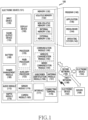
- Fig. 1 is a block diagram illustrating an electronic device 101 in a network environment 100 according to various embodiments.
- the electronic device 101 in the network environment 100 may communicate with an electronic device 102 via a first network 198 (e.g., a short-range wireless communication network), or at least one of an electronic device 104 or a server 108 via a second network 199 (e.g., a long-range wireless communication network).
- the electronic device 101 may communicate with the electronic device 104 via the server 108.
- the electronic device 101 may include a processor 120, memory 130, an input module 150, a sound output module 155, a display module 160, an audio module 170, a sensor module 176, an interface 177, a connecting terminal 178, a haptic module 179, a camera module 180, a power management module 188, a battery 189, a communication module 190, a subscriber identification module(SIM) 196, or an antenna module 197.
- at least one of the components e.g., the connecting terminal 178) may be omitted from the electronic device 101, or one or more other components may be added in the electronic device 101.
- some of the components e.g., the sensor module 176, the camera module 180, or the antenna module 197) may be implemented as a single component (e.g., the display module 160).
- the processor 120 may execute, for example, software (e.g., a program 140) to control at least one other component (e.g., a hardware or software component) of the electronic device 101 coupled with the processor 120, and may perform various data processing or computation. According to one embodiment, as at least part of the data processing or computation, the processor 120 may store a command or data received from another component (e.g., the sensor module 176 or the communication module 190) in volatile memory 132, process the command or the data stored in the volatile memory 132, and store resulting data in non-volatile memory 134.
- software e.g., a program 140
- the processor 120 may store a command or data received from another component (e.g., the sensor module 176 or the communication module 190) in volatile memory 132, process the command or the data stored in the volatile memory 132, and store resulting data in non-volatile memory 134.
- the processor 120 may include a main processor 121 (e.g., a central processing unit (CPU) or an application processor (AP)), or an auxiliary processor 123 (e.g., a graphics processing unit (GPU), a neural processing unit (NPU), an image signal processor (ISP), a sensor hub processor, or a communication processor (CP)) that is operable independently from, or in conjunction with, the main processor 121.
- a main processor 121 e.g., a central processing unit (CPU) or an application processor (AP)
- auxiliary processor 123 e.g., a graphics processing unit (GPU), a neural processing unit (NPU), an image signal processor (ISP), a sensor hub processor, or a communication processor (CP)
- the main processor 121 may be adapted to consume less power than the main processor 121, or to be specific to a specified function.
- the auxiliary processor 123 may be implemented as separate from, or as part of the main processor 121.
- the auxiliary processor 123 may control at least some of functions or states related to at least one component (e.g., the display module 160, the sensor module 176, or the communication module 190) among the components of the electronic device 101, instead of the main processor 121 while the main processor 121 is in an inactive (e.g., sleep) state, or together with the main processor 121 while the main processor 121 is in an active state (e.g., executing an application).
- the auxiliary processor 123 e.g., an image signal processor or a communication processor
- the auxiliary processor 123 may include a hardware structure specified for artificial intelligence model processing.
- An artificial intelligence model may be generated by machine learning. Such learning may be performed, e.g., by the electronic device 101 where the artificial intelligence is performed or via a separate server (e.g., the server 108). Learning algorithms may include, but are not limited to, e.g., supervised learning, unsupervised learning, semi-supervised learning, or reinforcement learning.
- the artificial intelligence model may include a plurality of artificial neural network layers.
- the artificial neural network may be a deep neural network (DNN), a convolutional neural network (CNN), a recurrent neural network (RNN), a restricted boltzmann machine (RBM), a deep belief network (DBN), a bidirectional recurrent deep neural network (BRDNN), deep Q-network or a combination of two or more thereof but is not limited thereto.
- the artificial intelligence model may, additionally or alternatively, include a software structure other than the hardware structure.
- the memory 130 may store various data used by at least one component (e.g., the processor 120 or the sensor module 176) of the electronic device 101.
- the various data may include, for example, software (e.g., the program 140) and input data or output data for a command related thererto.
- the memory 130 may include the volatile memory 132 or the non-volatile memory 134.
- the program 140 may be stored in the memory 130 as software, and may include, for example, an operating system (OS) 142, middleware 144, or an application 146.
- OS operating system
- middleware middleware
- application application
- the input module 150 may receive a command or data to be used by another component (e.g., the processor 120) of the electronic device 101, from the outside (e.g., a user) of the electronic device 101.
- the input module 150 may include, for example, a microphone, a mouse, a keyboard, a key (e.g., a button), or a digital pen (e.g., a stylus pen).
- the sound output module 155 may output sound signals to the outside of the electronic device 101.
- the sound output module 155 may include, for example, a speaker or a receiver.
- the speaker may be used for general purposes, such as playing multimedia or playing record.
- the receiver may be used for receiving incoming calls. According to an embodiment, the receiver may be implemented as separate from, or as part of the speaker.
- the display module 160 may visually provide information to the outside (e.g., a user) of the electronic device 101.
- the display module 160 may include, for example, a display, a hologram device, or a projector and control circuitry to control a corresponding one of the display, hologram device, and projector.
- the display module 160 may include a touch sensor adapted to detect a touch, or a pressure sensor adapted to measure the intensity of force incurred by the touch.
- the audio module 170 may convert a sound into an electrical signal and vice versa. According to an embodiment, the audio module 170 may obtain the sound via the input module 150, or output the sound via the sound output module 155 or a headphone of an external electronic device (e.g., an electronic device 102) directly (e.g., wiredly) or wirelessly coupled with the electronic device 101.
- an external electronic device e.g., an electronic device 102
- directly e.g., wiredly
- wirelessly e.g., wirelessly
- the sensor module 176 may detect an operational state (e.g., power or temperature) of the electronic device 101 or an environmental state (e.g., a state of a user) external to the electronic device 101, and then generate an electrical signal or data value corresponding to the detected state.
- the sensor module 176 may include, for example, a gesture sensor, a gyro sensor, an atmospheric pressure sensor, a magnetic sensor, an acceleration sensor, a grip sensor, a proximity sensor, a color sensor, an infrared (IR) sensor, a biometric sensor, a temperature sensor, a humidity sensor, or an illuminance sensor.
- the interface 177 may support one or more specified protocols to be used for the electronic device 101 to be coupled with the external electronic device (e.g., the electronic device 102) directly (e.g., wiredly) or wirelessly.
- the interface 177 may include, for example, a high definition multimedia interface (HDMI), a universal serial bus (USB) interface, a secure digital (SD) card interface, or an audio interface.
- HDMI high definition multimedia interface
- USB universal serial bus
- SD secure digital
- a connecting terminal 178 may include a connector via which the electronic device 101 may be physically connected with the external electronic device (e.g., the electronic device 102).
- the connecting terminal 178 may include, for example, a HDMI connector, a USB connector, a SD card connector, or an audio connector (e.g., a headphone connector).
- the haptic module 179 may convert an electrical signal into a mechanical stimulus (e.g., a vibration or a movement) or electrical stimulus which may be recognized by a user via his tactile sensation or kinesthetic sensation.
- the haptic module 179 may include, for example, a motor, a piezoelectric element, or an electric stimulator.
- the camera module 180 may capture a still image or moving images.
- the camera module 180 may include one or more lenses, image sensors, image signal processors, or flashes.
- the power management module 188 may manage power supplied to the electronic device 101.
- the power management module 188 may be implemented as at least part of, for example, a power management integrated circuit (PMIC).
- PMIC power management integrated circuit
- the battery 189 may supply power to at least one component of the electronic device 101.
- the battery 189 may include, for example, a primary cell which is not rechargeable, a secondary cell which is rechargeable, or a fuel cell.
- the communication module 190 may support establishing a direct (e.g., wired) communication channel or a wireless communication channel between the electronic device 101 and the external electronic device (e.g., the electronic device 102, the electronic device 104, or the server 108) and performing communication via the established communication channel.
- the communication module 190 may include one or more communication processors that are operable independently from the processor 120 (e.g., the application processor (AP)) and supports a direct (e.g., wired) communication or a wireless communication.
- AP application processor
- the communication module 190 may include a wireless communication module 192 (e.g., a cellular communication module, a short-range wireless communication module, or a global navigation satellite system (GNSS) communication module) or a wired communication module 194 (e.g., a local area network (LAN) communication module or a power line communication (PLC) module).
- a wireless communication module 192 e.g., a cellular communication module, a short-range wireless communication module, or a global navigation satellite system (GNSS) communication module
- GNSS global navigation satellite system
- wired communication module 194 e.g., a local area network (LAN) communication module or a power line communication (PLC) module.
- LAN local area network
- PLC power line communication
- a corresponding one of these communication modules may communicate with the external electronic device via the first network 198 (e.g., a short-range communication network, such as Bluetooth TM , wireless-fidelity (Wi-Fi) direct, or infrared data association (IrDA)) or the second network 199 (e.g., a long-range communication network, such as a legacy cellular network, a 5G network, a next-generation communication network, the Internet, or a computer network (e.g., LAN or wide area network (WAN)).
- first network 198 e.g., a short-range communication network, such as Bluetooth TM , wireless-fidelity (Wi-Fi) direct, or infrared data association (IrDA)
- the second network 199 e.g., a long-range communication network, such as a legacy cellular network, a 5G network, a next-generation communication network, the Internet, or a computer network (e.g., LAN or wide area network (WAN)).
- the wireless communication module 192 may identify and authenticate the electronic device 101 in a communication network, such as the first network 198 or the second network 199, using subscriber information (e.g., international mobile subscriber identity (IMSI)) stored in the subscriber identification module 196.
- subscriber information e.g., international mobile subscriber identity (IMSI)
- the antenna module 197 may transmit or receive a signal or power to or from the outside (e.g., the external electronic device) of the electronic device 101.
- the antenna module 197 may include an antenna including a radiating element composed of a conductive material or a conductive pattern formed in or on a substrate (e.g., a printed circuit board (PCB)).
- the antenna module 197 may include a plurality of antennas (e.g., array antennas). In such a case, at least one antenna appropriate for a communication scheme used in the communication network, such as the first network 198 or the second network 199, may be selected, for example, by the communication module 190 (e.g., the wireless communication module 192) from the plurality of antennas.
- the signal or the power may then be transmitted or received between the communication module 190 and the external electronic device via the selected at least one antenna.
- another component e.g., a radio frequency integrated circuit (RFIC)
- RFIC radio frequency integrated circuit
- At least some of the above-described components may be coupled mutually and communicate signals (e.g., commands or data) therebetween via an inter-peripheral communication scheme (e.g., a bus, general purpose input and output (GPIO), serial peripheral interface (SPI), or mobile industry processor interface (MIPI)).
- an inter-peripheral communication scheme e.g., a bus, general purpose input and output (GPIO), serial peripheral interface (SPI), or mobile industry processor interface (MIPI)
- commands or data may be transmitted or received between the electronic device 101 and the external electronic device 104 via the server 108 coupled with the second network 199.
- Each of the electronic devices 102 or 104 may be a device of a same type as, or a different type, from the electronic device 101.
- all or some of operations to be executed at the electronic device 101 may be executed at one or more of the external electronic devices 102, 104, or 108. For example, if the electronic device 101 should perform a function or a service automatically, or in response to a request from a user or another device, the electronic device 101, instead of, or in addition to, executing the function or the service, may request the one or more external electronic devices to perform at least part of the function or the service.
- the one or more external electronic devices receiving the request may perform the at least part of the function or the service requested, or an additional function or an additional service related to the request, and transfer an outcome of the performing to the electronic device 101.
- the electronic device 101 may provide the outcome, with or without further processing of the outcome, as at least part of a reply to the request.
- a cloud computing, distributed computing, mobile edge computing (MEC), or client-server computing technology may be used, for example.
- the electronic device 101 may provide ultra low-latency services using, e.g., distributed computing or mobile edge computing.
- the external electronic device 104 may include an internet-of-things (IoT) device.
- the server 108 may be an intelligent server using machine learning and/or a neural network.
- the external electronic device 104 or the server 108 may be included in the second network 199.
- the electronic device 101 may be applied to intelligent services (e.g., smart home, smart city, smart car, or healthcare) based on 5G communication technology or IoT-related technology.
- the electronic device may be one of various types of electronic devices.
- the electronic devices may include, for example, a portable communication device (e.g., a smartphone), a computer device, a portable multimedia device, a portable medical device, a camera, a wearable device, or a home appliance. According to an embodiment of the disclosure, the electronic devices are not limited to those described above.
- each of such phrases as “A or B,” “at least one of A and B,” “at least one of A or B,” “A, B, or C,” “at least one of A, B, and C,” and “at least one of A, B, or C,” may include any one of, or all possible combinations of the items enumerated together in a corresponding one of the phrases.
- such terms as “1st” and “2nd,” or “first” and “second” may be used to simply distinguish a corresponding component from another, and does not limit the components in other aspect (e.g., importance or order).
- an element e.g., a first element
- the element may be coupled with the other element directly (e.g., wiredly), wirelessly, or via a third element.
- module may include a unit implemented in hardware, software, or firmware, and may interchangeably be used with other terms, for example, “logic,” “logic block,” “part,” or “circuitry”.
- a module may be a single integral component, or a minimum unit or part thereof, adapted to perform one or more functions.
- the module may be implemented in a form of an application-specific integrated circuit (ASIC).
- ASIC application-specific integrated circuit
- Various embodiments as set forth herein may be implemented as software (e.g., the program 140) including one or more instructions that are stored in a storage medium (e.g., internal memory 136 or external memory 138) that is readable by a machine (e.g., the electronic device 101).
- a processor e.g., the processor 120
- the machine e.g., the electronic device 101
- the one or more instructions may include a code generated by a complier or a code executable by an interpreter.
- the machine-readable storage medium may be provided in the form of a non-transitory storage medium.
- non-transitory simply means that the storage medium is a tangible device, and does not include a signal (e.g., an electromagnetic wave), but this term does not differentiate between where data is semi-permanently stored in the storage medium and where the data is temporarily stored in the storage medium.
- a method may be included and provided in a computer program product.
- the computer program product may be traded as a product between a seller and a buyer.
- the computer program product may be distributed in the form of a machine-readable storage medium (e.g., compact disc read only memory (CD-ROM)), or be distributed (e.g., downloaded or uploaded) online via an application store (e.g., PlayStore TM ), or between two user devices (e.g., smart phones) directly. If distributed online, at least part of the computer program product may be temporarily generated or at least temporarily stored in the machine-readable storage medium, such as memory of the manufacturer's server, a server of the application store, or a relay server.
- CD-ROM compact disc read only memory
- an application store e.g., PlayStore TM
- two user devices e.g., smart phones
- each component e.g., a module or a program of the above-described components may include a single entity or multiple entities, and some of the multiple entities may be separately disposed in different components. According to various embodiments, one or more of the above-described components may be omitted, or one or more other components may be added. Alternatively or additionally, a plurality of components (e.g., modules or programs) may be integrated into a single component. In such a case, according to various embodiments, the integrated component may still perform one or more functions of each of the plurality of components in the same or similar manner as they are performed by a corresponding one of the plurality of components before the integration.
- operations performed by the module, the program, or another component may be carried out sequentially, in parallel, repeatedly, or heuristically, or one or more of the operations may be executed in a different order or omitted, or one or more other operations may be added.
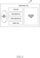
- Fig. 2 is a block diagram 200 illustrating the camera module 180 according to various embodiments.
- the camera module 180 may include a lens assembly 210, a flash 220, an image sensor 230, an image stabilizer 240, memory 250 (e.g., buffer memory), or an image signal processor 260.
- the lens assembly 210 may collect light emitted or reflected from an object whose image is to be taken.
- the lens assembly 210 may include one or more lenses.
- the camera module 180 may include a plurality of lens assemblies 210. In such a case, the camera module 180 may form, for example, a dual camera, a 360-degree camera, or a spherical camera.
- Some of the plurality of lens assemblies 210 may have the same lens attribute (e.g., view angle, focal length, auto-focusing, f number, or optical zoom), or at least one lens assembly may have one or more lens attributes different from those of another lens assembly.
- the lens assembly 210 may include, for example, a wide-angle lens or a telephoto lens.
- the flash 220 may emit light that is used to reinforce light reflected from an object.
- the flash 220 may include one or more light emitting diodes (LEDs) (e.g., a red-green-blue (RGB) LED, a white LED, an infrared (IR) LED, or an ultraviolet (UV) LED) or a xenon lamp.
- LEDs light emitting diodes
- the image sensor 230 may obtain an image corresponding to an object by converting light emitted or reflected from the object and transmitted via the lens assembly 210 into an electrical signal.
- the image sensor 230 may include one selected from image sensors having different attributes, such as a RGB sensor, a black-and-white (BW) sensor, an IR sensor, or a UV sensor, a plurality of image sensors having the same attribute, or a plurality of image sensors having different attributes.
- Each image sensor included in the image sensor 230 may be implemented using, for example, a charged coupled device (CCD) sensor or a complementary metal oxide semiconductor (CMOS) sensor.
- CCD charged coupled device
- CMOS complementary metal oxide semiconductor
- the image stabilizer 240 may move the image sensor 230 or at least one lens included in the lens assembly 210 in a particular direction, or control an operational attribute (e.g., adjust the read-out timing) of the image sensor 230 in response to the movement of the camera module 180 or the electronic device 101 including the camera module 180. This allows compensating for at least part of a negative effect (e.g., image blurring) by the movement on an image being captured.
- the image stabilizer 240 may sense such a movement by the camera module 180 or the electronic device 101 using a gyro sensor (not shown) or an acceleration sensor (not shown) disposed inside or outside the camera module 180.
- the image stabilizer 240 may be implemented, for example, as an optical image stabilizer.
- the memory 250 may store, at least temporarily, at least part of an image obtained via the image sensor 230 for a subsequent image processing task. For example, if image capturing is delayed due to shutter lag or multiple images are quickly captured, a raw image obtained (e.g., a Bayer-patterned image, a high-resolution image) may be stored in the memory 250, and its corresponding copy image (e.g., a low-resolution image) may be previewed via the display module 160. Thereafter, if a specified condition is met (e.g., by a user's input or system command), at least part of the raw image stored in the memory 250 may be obtained and processed, for example, by the image signal processor 260. According to an embodiment, the memory 250 may be configured as at least part of the memory 130 or as a separate memory that is operated independently from the memory 130.
- a raw image obtained e.g., a Bayer-patterned image, a high-resolution image
- its corresponding copy image e.g., a low-
- the image signal processor 260 may perform one or more image processing with respect to an image obtained via the image sensor 230 or an image stored in the memory 250.
- the one or more image processing may include, for example, depth map generation, three-dimensional (3D) modeling, panorama generation, feature point extraction, image synthesizing, or image compensation (e.g., noise reduction, resolution adjustment, brightness adjustment, blurring, sharpening, or softening).
- the image signal processor 260 may perform control (e.g., exposure time control or read-out timing control) with respect to at least one (e.g., the image sensor 230) of the components included in the camera module 180.
- An image processed by the image signal processor 260 may be stored back in the memory 250 for further processing, or may be provided to an external component (e.g., the memory 130, the display module 160, the electronic device 102, the electronic device 104, or the server 108) outside the camera module 180.
- the image signal processor 260 may be configured as at least part of the processor 120, or as a separate processor that is operated independently from the processor 120. If the image signal processor 260 is configured as a separate processor from the processor 120, at least one image processed by the image signal processor 260 may be displayed, by the processor 120, via the display module 160 as it is or after being further processed.
- the electronic device 101 may include a plurality of camera modules 180 having different attributes or functions.
- at least one of the plurality of camera modules 180 may form, for example, a wide-angle camera and at least another of the plurality of camera modules 180 may form a telephoto camera.
- at least one of the plurality of camera modules 180 may form, for example, a front camera and at least another of the plurality of camera modules 180 may form a rear camera.
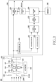
- FIG. 3 is a block diagram illustrating a camera module 300 according to an embodiment.
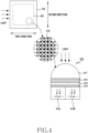
- FIG. 4 is a diagram illustrating photodiodes 410 of an image sensor 310 according to an embodiment.
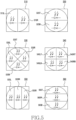
- FIG. 5 is a diagram illustrating an array of sub photodiodes of a photodiode according to an embodiment.
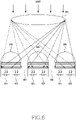
- FIG. 6 is a diagram illustrating an amount of incident light to photodiodes 610, 620 and 630 according to an embodiment.
- FIG. 7A is a diagram illustrating a raw image acquired by a camera module 300 according to an embodiment.
- FIG. 7B is a diagram illustrating a first luminance image acquired by first sub photodiodes 415L of the camera module 300 according to an embodiment.
- FIG. 7C is a diagram illustrating a second luminance image acquired by second sub photodiodes 415R of the camera module 300 according to an embodiment.
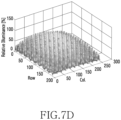
- FIG. 7D is a graph showing luminance values of pixels of the first luminance image.
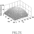
- FIG. 7E is a graph showing luminance values of pixels of the second luminance image.
- FIG. 7F is a graph showing a raw luminance ratio between the luminance values of the pixels of the first luminance image and the luminance values of the pixels of the second luminance image.
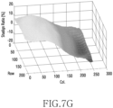
- FIG. 7G is a graph showing a luminance ratio obtained by reducing noise of the raw luminance ratio.
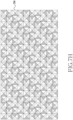
- FIG. 7H is a diagram illustrating an image image-signal-processed by the camera module 300 according to an embodiment.
- the camera module 300 may correspond to the camera module 180 of FIG. 1 and FIG. 2 .
- the camera module 300 may include an image acquisition module 301, an image signal processor 305, a memory 395, or a combination thereof.
- the image signal processor 305 may correspond to the image signal processor 260 of FIG. 2 .
- the memory 395 may correspond to the memory 250 of FIG. 2 .
- the memory 395 may store a plurality of reference luminance ratios corresponding to different optical characteristics (e.g., an F value, a position of a lens 330, or a tilting degree of the lens 330) respectively.
- the reference luminance ratio may be a ratio of luminance values between at least two sub images with respect to a reference image pre-acquired to have arbitrary optical characteristics.
- the image acquisition module 301 may include an image sensor 310, an aperture 320, a lens 330, an actuator 340, or a combination thereof.
- the aperture 320 is positioned in front of the lens 330 (e.g., in a direction relatively close to light), but it is only an example.
- the aperture 320 may be positioned between the lens 330 and the image sensor 310.
- the lens 330 may include one or more lenses.
- the image sensor 310 may correspond to the image sensor 230 of FIG. 2 .
- the lens 330 may be included in the lens assembly 210 of FIG. 2 .
- the image signal processor 305 may include an image correction unit 350, a detection unit 355, a preprocessing unit 360, noise reduction units 371, 375, and 379, a ratio calculation unit 380, a matching unit 390, or a combination thereof.
- the image correction unit 350, the detection unit 355, the preprocessing unit 360, the noise reduction units 371, 375, and 379, the ratio calculation unit 380, the matching unit 390, or a combination thereof may be implemented through a hardware circuit.
- the image correction unit 350, the detection unit 355, the preprocessing unit 360, the noise reduction units 371, 375, and 379, the ratio calculation unit 380, the matching unit 390, or a combination thereof may be implemented in software operable by the image signal processor 305.
- FIG. 3 illustrates that two noise reduction units 371 and 375 are connected between the preprocessing unit 360 and the ratio calculation unit 380, but this is only an example.
- the number of noise reduction units connected between the preprocessing unit 360 and the ratio calculation unit 380 may correspond to the number of sub photodiodes constituting each of a plurality of photodiodes included in the image sensor 310.
- the noise reduction units connected between the preprocessing unit 360 and the ratio calculation unit 380 may reduce noise of outputs of the corresponding sub photodiodes respectively. For example, if the number of sub photodiodes constituting each of the plurality of the photodiodes is 4, the number of the noise reduction units connected between the preprocessing unit 360 and the ratio calculation unit 380 may be 4. In an embodiment, some of the components illustrated in FIG. 3 may be omitted. For example, one or more noise reduction units of the noise reduction units 371, 375, and 379 may be omitted.
- the output of the preprocessing unit 360 may be inputted to the ratio calculation unit 380.
- the output of the ratio calculation unit 380 may be inputted to the matching unit 390.
- the aperture 320 may adjust a size of an entrance pupil, under control of the image signal processor 305. In an embodiment, as the size of the entrance pupil of the aperture 320 increases, the amount of light reaching the image sensor 310 may increase. In an embodiment, if the size of the entrance pupil of the aperture 320 decreases, the light amount reaching the image sensor 310 may decrease.
- the lens 330 may collect incident light through the aperture 320.
- the actuator 340 may move the lens 330 to one of different positions 331 through 339, under control of the image signal processor 305.
- the image sensor 310 may detect a signal corresponding to the light passing through the aperture 320 and the lens 330.
- the image sensor 310 may include an array 401 of photo diodes (PDs).
- the array 401 may include a plurality of PDs 410.
- the array 401 may be positioned on a plane perpendicular to the Z axis corresponding to a direction in which light is incoming.
- a first direction (e.g., the X-axis direction) of the array 401 may be perpendicular to a second direction (e.g., the Y-axis direction) of the array 401.
- the first direction (e.g., the X-axis direction) and the second direction e.g., the Y-axis direction
- the first direction e.g., the X-axis direction
- the second direction e.g., the Y-axis direction
- the plurality of the PDs 410 each may include a micro lens 411, an infrared cut-off filter 412, a color filter 413, an antireflection film 414, at least two sub PDs 415L and 415R, or a combination thereof.
- the plurality of the PDs 410 each may also be referred to as a light receiving element.
- each of the at least two sub PDs of each of the PDs 410 may be referred to as a sub light receiving element.
- a PD including at least two sub PDs may also be referred to as a multi-PD.
- the micro lens 411 may condense incident light to the micro lens 411. In an embodiment, the micro lens 411 may adjust a path of the incident light on the micro lens 411 such that the light reaches the first sub PD 415L and the second sub PD 415R.
- the infrared cut-off filter 412 may block infrared ray of at least part of the incident light through the micro lens 411.
- the color filter 413 may pass light of a predesignated color (or, color channel).
- the color filter 413 of each of the plurality of the PDs 410 may pass light of one color (e.g., red) of predesignated colors (e.g., red, blue, or green), according to a predesignated pattern (e.g., Bayer pattern).
- the color filter 413 may block light of other color than the predesignated color (or, color channel).
- the antireflection layer 414 may prevent the incident light through the micro lens 411 from being reflected to outside.
- the first sub PD 415L and the second sub PD 415R may output a value corresponding to the incident light. In an embodiment, the first sub PD 415L and the second sub PD 415R may output a value corresponding to the incident light based on a photoelectric effect. In an embodiment, the first sub PD 415L and the second sub PD 415R may output a value corresponding to an intensity (or, illuminance) of the incident light based on the photoelectric effect.
- the first sub PD 415L and the second sub PD 415R may generate charges according to the intensity (or, illuminance) of the incident light based on the photoelectric effect. In an embodiment, the first sub PD 415L and the second sub PD 415R may output a current according to an amount of the generated charges. In an embodiment, the value outputted from the first sub PD 415L may also be referred to as a first sensing value. In an embodiment, the value outputted from the second sub PD 415R may also be referred to as a second sensing value.
- FIG. 4 it is illustrated that the two sub PDs 415L and 415R are disposed on the left side and the right side of one PD 410, but this is only an example. Two or more sub PDs may be included in one PD 410 at different positions.
- a PD 510 may include a first sub PD 515L disposed on the left side and a second sub PD 515R disposed on the right side.
- light having different phases, and/or different intensities (or illuminances) may enter the sub PDs 515L and 515R disposed left and right in a horizontal direction.
- a photodiode 520 may include a first sub PD 525T disposed at an upper side and a second sub PD 525B disposed at a lower side.
- light having different phases, and/or different intensities (or illuminances) may enter the sub PDs 525T and 525B disposed up and down in a vertical direction.
- a PD 530 may include a first sub PD 535T disposed on an upper side, a second sub PD 535B disposed on a lower side, a third sub PD 535L disposed on a left side, and a fourth sub PD 535R disposed on a right side.
- the four sub PDs 535T, 535B, 535L, and 535R may receive light having different phases, and/or different intensities (or illuminances) in a horizontal direction and/or a vertical direction.
- one pair of the sub PDs 535T and 535L and the other pair of the sub PDs 535B and 535R among the four sub PDs 535T, 535B, 535L, and 535R may receive light having different phases, and/or different intensities (or illuminances) in a first diagonal direction.
- one pair of the sub PDs 535B and 535L and the other pair of the sub PDs 535T and 535R among the four sub PDs 535T, 535B, 535L, and 535R may receive light having different phases, and/or different intensities (or illuminances) in a second diagonal direction.
- the first diagonal direction and the second diagonal direction may be perpendicular to each other.
- a PD 540 may include a first sub PD 545LT disposed on an upper left side, a second sub PD 545RT disposed on an upper right side, a third sub PD 545LB disposed on a lower left side, and a fourth sub PD 545RB disposed on a lower right side.
- the four sub PDs 545LT, 545RT, 545LB, and 545RB may receive light having different phases, and/or different intensities (or illuminances) in the horizontal direction and/or the vertical direction.
- the sub PDs 545LT and 545RB positioned in an oblique direction among the four sub PDs 545LT, 545RT, 545LB, and 545RB may receive the light having different phases, and/or different intensities (or illuminances) in a third diagonal direction.
- the sub PDs 545RT and 545LB positioned in the oblique direction among the four sub PDs 545LT, 545RT, 545LB, and 545RB may receive the light having different phases, and/or different intensities (or illuminances) in a fourth diagonal direction.
- the third diagonal direction and the fourth diagonal direction may be perpendicular to each other.
- a PD 550 may include a first sub PD 555L disposed on a left side, a second sub PD 555M disposed at the center, and a third sub PD 555R disposed on a right side based on the horizontal direction.
- the three sub PDs 555L, 555M, and 555R may receive light having different phases, and/or different intensities (or illuminances) in the horizontal direction.
- a PD 560 may include a first sub PD 565T disposed at an upper side, a second sub PD 565M disposed at the center, and a third sub PD 555B disposed at a lower side along the vertical direction.
- the three sub PDs 565T, 565M, and 565B may receive light having different phases, and/or different intensities (or illuminances) in the horizontal direction.
- the sub PDs 415L and 415R may output values indicating different light intensities.
- light may enter PDs 610, 620, and 630 after passing through the lens 330.
- the intensity (or illuminance) of the incident light to the PDs 610, 620, and 630 varies, depending on a position in the lens 330 through which the light passes.
- one or more PDs 641 may be disposed, between the PDs 610 and 620.
- one or more PDs 645 may be disposed, between the PDs 620 and 630.
- light of different light amounts may enter the sub PDs 611 and 615 of the PD 610.
- an area in which the light passing through the left portion of the lens 330 enters the sub PD 615 of the PD 610 may be smaller than an area entering the sub PD 611 of the PD 610.
- an area in which the light passing through the right portion of the lens 330 enters the sub PD 631 of the PD 630 may be smaller than an area entering the sub PD 635 of the PD 630.
- the intensity of the incident light may differ between the sub PDs 611, 615, 621, 625, 631, and 635 of each of the PDs 610, 620, and 630 according to the positions of the PDs 610, 620, and 630.
- outputs of the sub PDs 611 and 615 may be different.
- outputs of the sub PDs 621 and 625 may be different.
- outputs of the sub PDs 631 and 635 may be different.
- the image sensor 310 may provide a value corresponding to the detected light intensity to the image signal processor 305.
- the image sensor 310 may provide the image signal processor 350 with the first sensing value outputted by the first sub PD 415L and the second sensing value outputted by the second sub PD 415R of each of the PDs 410.
- the image sensor 310 may provide the image signal processor 305 with a sum value of the first sensing value outputted by the first sub PD 415L and the second sensing value outputted by the second sub PD 415R of each of the PDs 410.
- the image sensor 310 may also provide a low-resolution luminance signal to the image signal processor 305.
- the low-resolution luminance signal may correspond to a sum value of outputs of adjacent photodiodes in the PDs 410.
- the adjacent PDs may be PDs assigned different colors among the adjacent PDs.
- the preprocessing unit 360 may output a luminance signal, based on data (e.g., the first sensing value, and the second sensing value, or the sum value and the low-resolution luminance signal) from the image sensor 310. In an embodiment, the preprocessing unit 360 may output a first luminance signal corresponding to the first sensing value outputted by the first sub PD 415L of each of the PDs 410. In an embodiment, the preprocessing unit 360 may output a second luminance signal corresponding to the second sensing value outputted by the second sub PD 415R of each of the PDs 410.
- the sum value of the value outputted by the first sub PD 415L and the value outputted by the second sub PD 415R of each of the PDs 410 may correspond to a raw image 701.
- the raw image 701 may be an image obtained by adding a first raw sub image indicated by the value outputted by the first sub PD 415L, and a second raw sub image indicated by the value outputted by the second sub PD 415R of each of the PDs 410.
- the position of each of the PDs 410 may be identified based on the image (e.g., the raw image 701).
- the positions of the first sub PD 415L and the second sub PD 415R of each of the PDs 410 may be identified based on the image (e.g., the raw image 701). For example, if there is any other pixel adjacent to the left of a random pixel among pixels constituting the image (e.g., the raw image 701), the PD 410 corresponding to any other pixel may be identified as being positioned on the left side of the PD 410 corresponding to the random pixel.
- a sub PD adjacent to the PD 410 corresponding to the random pixel among the first sub PD 415L and the second sub PD 415R of the PD 410 corresponding to any other pixel may be identified as being positioned on the left from other sub PDs.
- the first luminance signal may correspond to a first luminance image 702.
- the second luminance signal may correspond to a second luminance image 703.
- the first luminance image 702 may correspond to the value outputted by the first sub PD 415L positioned at a first position (e.g., a left position of each of the PDs 410) corresponding in each of the PDs 410.
- the second luminance image 703 may correspond to the value outputted by the second sub PD 415R positioned at a second position (e.g., a right position of each of the PDs 410) corresponding in each of the PDs 410.
- the first position and the second position may be different positions in each of the PDs 410.
- a left region 710 of the first luminance image 702 may be relatively brighter than a right region 720.
- the right region 720 of the second luminance image 703 may be relatively brighter than the left region 710.
- pixels positioned in the left region 710 of the first luminance image 702 may have higher luminance values than pixels positioned in the left region 710 of the second luminance image 703.
- pixels positioned in the right region 720 of the second luminance image 703 may have higher luminance values than pixels positioned in the right region 720 of the first luminance image 702.
- the luminance value of each of the pixels of the raw image 701 may correspond to the light intensity identified by each of the PDs 410.
- the preprocessing unit 360 may provide the first luminance image 702 and the second luminance image 703 to the noise reduction unit 371 or 375. In an embodiment, the preprocessing unit 360 may provide the first luminance image 702 to the noise reduction unit 371. In an embodiment, the preprocessing unit 360 may provide the second luminance image 703 to the noise reduction unit 375.
- the noise reduction units 371 and 375 each may reduce noise of the inputted data (e.g., the first luminance image 702 or the second luminance image 703). In an embodiment, the noise reduction units 371 and 375 each may provide noise-reduced data to the ratio calculation unit 380.
- the noise reduction units 371 and 375 each may reduce the noise, by attenuating a high frequency component of the inputted data, using a method of binning, averaging, interpolation, low pass filtering, or a combination thereof.
- the inputted data may be out of phase, and the noise reduction units 371 and 375 each may reduce the noise according to the phase, by correcting a phase difference using the method of the binning, the averaging, the interpolation, the low pass filtering or a combination thereof.
- the ratio calculation unit 380 may calculate a raw luminance ratio of the noise-reduced data (e.g., the first luminance image 702 and the second luminance image 703 with the noise reduced) from the noise reduction units 371 and 375.
- the ratio calculation unit 380 may calculates a raw luminance ratio between luminance values of pixels at corresponding positions among the pixels of the first luminance image 702 and the second luminance image 703 with the noise reduced. In an embodiment, the ratio calculation unit 380 may calculate a raw luminance ratio between a luminance value of an i-th pixel of the noise-reduced first luminance image 702 and a luminance value of a i-th pixel of the noise-reduced second luminance image 703. In an embodiment, i may be an integer which is equal to or greater than 1 and equal to or less than the number of the pixels of the first luminance image 702 (or the second luminance image 703).
- SR0(i) may denote the raw luminance ratio between the luminance value of the i-th pixel of the noise-reduced first luminance image 702 and the luminance value of the i-th pixel of the noise-reduced second luminance image 703.
- Y1(i) may denote the luminance value of the i-th pixel of the first luminance image 702.
- Y2(i) may denote the luminance value of the i-th pixel of the second luminance image 703.
- SR0(i) may denote the raw luminance ratio between the luminance value of the i-th pixel of the noise-reduced first luminance image 702 and the luminance value of the i-th pixel of the noise-reduced second luminance image 703.
- Y1(i) may denote the luminance value of the i-th pixel of the first luminance image 702.
- Y2(i) may denote the luminance value of the i-th pixel of the second luminance image 703.
- luminance images may be generated in the predesignated number.
- SR0jk(i) may denote a raw luminance ratio between a luminance value of an i-th pixel of a j-th luminance image and a luminance value of an i-th pixel of a k-th luminance image among the predesignated number of the noise-reduced luminance images.
- Yj(i) may denote the luminance value of the i-th pixel of the j-th luminance image.
- Yk(i) may denote the luminance value of the i-th pixel of the k-th luminance image.
- the j-th luminance image may be an image generated by a sensing value of the j-th sub PD of each of the PDs.
- the k-th luminance image may be an image generated by a sensing value of the k-th sub PD of each of the PDs.
- SR0jk(i) may denote the raw luminance ratio between the luminance value of the i-th pixel of the j-th luminance image and the luminance value of the i-th pixel of the k-th luminance image among the predesignated number of the noise-reduced luminance images.
- Yj(i) may denote the luminance value of the i-th pixel of the j-th luminance image.
- Yk(i) may denote the luminance value of the i-th pixel of the k-th luminance image.
- the j-th luminance image may be an image generated by the sensing value of the j-th sub PD of each of the PDs.
- the k-th luminance image may be an image generated by the sensing value of the k-th sub PD of each of the PDs.
- the ratio calculation unit 380 may calculate the raw luminance ratios of the luminance values of the pixels of the first luminance image 702 as shown in FIG. 7D and the luminance values of the pixels of the second luminance image 703 as shown in FIG. 7E , as shown in FIG. 7F .
- luminance values of pixels of a portion corresponding to columns of a left portion may be greater than luminance values of pixels of a portion corresponding to columns of a right portion in the first luminance image 702.
- luminance values of pixels in a portion corresponding to columns of a right portion may be greater than luminance values of pixels in a portion corresponding to columns of a left portion in the second luminance image 703.
- FIG. 7F as the columns increase from the left to the right, the first ratio tends to decrease.
- the ratio calculation unit 380 may provide the calculated raw luminance ratio to the noise reduction unit 379.
- the noise reduction unit 379 may reduce noise due to the color of the subject by using a method of tuning, averaging, low pass filtering, or a combination thereof with respect to the raw luminance ratio. In an embodiment, the noise reduction unit 379 may reduce noise due to the color of the subject for each of the raw luminance ratios corresponding to the PDs 410 assigned the same color among the raw luminance ratios.
- the noise of the raw luminance ratio identified in FIG. 7F is reduced by the noise reduction unit 379.
- the noise reduction unit 379 may provide the matching unit 390 with the noise-reduced luminance ratio with respect to the raw luminance ratio.
- the matching unit 390 may identify a reference luminance ratio corresponding to optical characteristics (e.g., an F value, a lens position, or a lens tilting degree) in acquiring the raw image 701 among the reference ratios stored in the memory 395.
- the matching unit 390 may identify the reference luminance ratio, by comparing the reference luminance ratios stored in the memory 395 with the luminance ratio.
- the identified reference luminance ratio may be a reference luminance ratio having the smallest difference from the luminance ratio among the plurality of the reference luminance ratios.
- the matching unit 390 may identify the reference luminance ratio corresponding to the optical characteristics (e.g., an F value, a lens position, or a lens tilting degree) in acquiring the raw image 701, based on information indicating the optical characteristics of the identified reference luminance ratio.
- the optical characteristics e.g., an F value, a lens position, or a lens tilting degree
- ⁇ SR(i) may denote a difference value between the luminance ratio of the i-th pixel and the identified reference luminance ratio.
- ⁇ SR(i) may correspond to an absolute value of the difference value between the luminance ratio of the i-th pixel and the identified reference luminance ratio.
- SR(i) may denote a luminance ratio with the noise removed.
- SRref(i) may denote the reference luminance ratio of the i-th pixel.
- the matching unit 390 may provide the detection unit 355 with information of the luminance ratio, the identified reference luminance ratio, the difference value, or a combination thereof.
- the detection unit 355 may detect at least one defect (or, noise) in the raw image 701, based on the information of the luminance ratio, the identified reference luminance ratio, the difference value, or a combination thereof.
- the defect (or, noise) may be caused by a flare due to a light source of high luminous intensity, saturation of the image sensor 310, a foreign substance of the lens 330, or a combination thereof.
- ⁇ SR(i) may denote a difference value between a second ratio of the i-th pixel of the pixels of the raw image 701 and the identified reference ratio.
- N may correspond to the number of the pixels of the raw image 701.
- SRfo may denote a predesignated reference average value.
- the detection unit 355 may detect the defect (or, noise) caused by the flare in the raw image 701, based on the difference value ⁇ SR(i). In an embodiment, if the difference value ⁇ SR(i) is greater than the predesignated reference difference value, the detection unit 355 may determine the defect (or, noise) due to the flare in the raw image 701. In an embodiment, the detection unit 355 may determine a pixel having the difference value ⁇ SR(i) greater than the predesignated reference difference value among the pixels of the raw image 701 as a pixel having the defect (or, noise) caused by the flare. In an embodiment, the detection unit 355 may determine the pixel having the difference value ⁇ SR(i) which satisfies the following Equation 7 as the pixel having the defect (or, noise) caused by the flare. ⁇ SR i > SR fl
- ⁇ SR(i) may denote the difference value between the luminance ratio of the i-th pixel among the pixels of the raw image 701 and the identified reference luminance ratio.
- SRfl may denote the predesignated reference difference value.
- the detection unit 355 may detect a defect (or, noise) due to the saturation in the raw image 701, based on the difference value ⁇ SR(i).
- the luminance ratio of each of the pixels of the raw image 701 may be equal to the reference luminance ratio, until at least one sub PD of the sub PDs 415L and 415R included in each of the PDs 410 is saturated.
- both of the two sub PDs 415L and 415R may be unsaturated, one sub PD of the two sub PDs 415L and 415R may be saturated and the other sub PD may be unsaturated, or both of the two sub PDs 415L and 415R may be saturated.
- the relationship depending on whether each of the two sub PDs 415L and 415R is saturated may be expressed as the following Equation 8 or Equation 9.
- Equation 8 may express the change of the luminance ratio according to the increase of the light amount, if the light amount recognized by the first sub PD 415L among the sub PDs 415L and 415R of the PD 410 is less than the light amount recognized by the second sub PD 415R.
- SRref (i) may denote the reference luminance ratio of the i-th pixel.
- SR1(i) may denote the luminance ratio of the i-th pixel corresponding to the corresponding PD 410, if all of the sub PDs 415L and 415R are unsaturated.
- SR2(i) may denote the luminance ratio of the i-th pixel corresponding to the corresponding PD 410, if the second sub PD 415R is saturated and the first sub PD 415L is unsaturated.
- SR3(i) may denote the luminance ratio of the i-th pixel corresponding to the corresponding PD 410, if all of the sub PDs 415L and 415R are saturated.
- Equation 9 may express the change of the luminance ratio according to the increase of the light amount, if the light amount recognized by the first sub PD 415L among the sub PDs 415L and 415R of the PD 410 is greater than the light amount recognized by the second sub PD 415R.
- SRref (i) may denote the reference luminance ratio of the i-th pixel.
- SR1(i) may denote the luminance ratio of the i-th pixel corresponding to the corresponding PD 410, if all of the sub PDs 415L and 415R are unsaturated.
- SR2(i) may denote the luminance ratio of the i-th pixel corresponding to the corresponding PD 410, if the first sub PD 415RL is saturated and the second sub PD 415R is unsaturated.
- SR3(i) may denote the luminance ratio of the i-th pixel corresponding to the corresponding PD 410, if all of the sub PDs 415L and 415R are saturated.
- the luminance ratio of the pixel corresponding to the corresponding PD 410 may be equal to the reference luminance ratio. In an embodiment, referring to Equation 8 and Equation 9, if all of the sub PDs 415L and 415R have the saturation state, the luminance ratio of the pixel corresponding to the corresponding PD 410 may be equal to 1.
- the luminance ratio of the pixel corresponding to the corresponding PD 410 may have a value between the reference luminance ratio and 1. In an embodiment, the luminance ratio may be greater than 1, or smaller than 1.
- the difference value ⁇ SR(i) may have a value between 0 and a value acquired by subtracting the reference luminance ratio from 1, if the reference luminance ratio is 1 or less, or may have a value between 0 and a value acquired by subtracting 1 from the reference luminance ratio, if the reference luminance ratio exceeds 1.
- the detection unit 355 may identify a saturation level of the pixel having the corresponding difference value ⁇ SR(i) depending on which one of the value of 0, the value between 0 and the value obtained by subtracting the reference luminance ratio from 1, or the value obtained by subtracting the reference luminance ratio from 1 the difference value ⁇ SR(i) corresponds to.
- the detection unit 355 may determine a pixel of which the difference value ⁇ SR(i) has other value than 0 as the pixel having the defect (or, noise) due to the saturation.
- the detection unit 355 may estimate the luminance of the pixel having the defect (or, noise) due to the saturation.
- Equation 10 may be the equation for estimating the luminance value of the pixel having the defect (or, noise) due to the saturation, if the light amount recognized by the first sub PD 415L among the sub PDs 415L and 415R of the PD 410 is less than the light amount recognized by the second sub PD 415R, and the second sub PD 415R is saturated (i.e., if the luminance value Y2(i) of the i-th pixel of the second luminance image 703 has the saturation state value).
- Y(i) may denote the luminance value of the i-th pixel of the raw image 701.
- Equation 10 Y1(i) may denote the luminance value of the i-th pixel of the first luminance image 702.
- SRref(i) may denote the reference luminance ratio of the i-th pixel.
- Y i Y 2 i ⁇ 1 + 1 SR ref i
- Equation 11 may be the equation for estimating the luminance value of the pixel having the defect (or, noise) due to the saturation, if the light amount recognized by the second sub PD 415R among the sub PDs 415L and 415R of the PD 410 is less than the light amount recognized by the first sub PD 415L, and the first sub PD 415L is saturated (i.e., if the luminance value Y1(i) of the i-th pixel of the first luminance image 702 has the saturation state value).
- Y(i) may denote the luminance value of the i-th pixel of the raw image 701.
- Y2(i) may denote the luminance value of the i-th pixel of the second luminance image 703.
- SRref(i) may denote the reference luminance ratio of the i-th pixel.
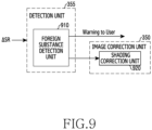
- the detection unit 355 may transmit information of at least one defect (or, noise) detected in the raw image 701 to other component (e.g., the image correction unit 350, the processor 120 of FIG. 1 , the application 146 of FIG. 1 ) of the electronic device 201.
- other component e.g., the image correction unit 350, the processor 120 of FIG. 1 , the application 146 of FIG. 1
- the detection unit 355 may transmit the estimated luminance value of the pixel having at least one defect (or, noise) due to the saturation detected in the raw image 701 to other component (e.g., the image correction unit 350, the processor 120 of FIG. 1 , the application 146 of FIG. 1 ) of the electronic device 201.
- other component e.g., the image correction unit 350, the processor 120 of FIG. 1 , the application 146 of FIG. 1
- the image correction unit 350 may correct the value of each of the pixels of the raw image 701, based on the information of at least one defect (or, noise). In an embodiment, the image correction unit 350 may correct the values of the pixels of the first raw sub image and the second raw sub image, based on the information of at least one defect (or, noise).
- the image correction unit 350 may correct the values of the pixels of the raw image 701, based on a correction value corresponding to the luminance ratio of each of the pixels of the raw image 701. In an embodiment, if the raw image 701 has the defect (or, noise) due to the foreign substance, the image correction unit 350 may correct the values of the pixels of the raw image 701, based on a correction value corresponding to the difference value ⁇ SR(i) of each of the pixels of the raw image 701.
- the image correction unit 350 may correct a pixel value having the defect (or, noise) due to the flare, based on values of pixels around the pixel having the defect (or, noise) due to the flare. In an embodiment, the image correction unit 350 may correct the pixel value having the defect (or, noise) due to the flare, based on values of high-reliability pixels among the pixels around the pixel having the defect (or, noise) due to the flare. In an embodiment, the reliability of the pixels may be determined in response to the difference value ⁇ SR(i) of the pixels. In an embodiment, the image correction unit 350 may identify as the pixel having high reliability as the difference value ⁇ SR(i) is close to 0. In an embodiment, the image correction unit 350 may identify as the pixel having low reliability as the difference value ⁇ SR(i) is far from 0.
- the image correction unit 350 may determine an average value of the values of the pixels around the pixel having the defect (or, noise) due to the flare, as the value of the pixel having the defect (or, noise) due to the flare. In an embodiment, the image correction unit 350 may correct an average value of values of high-reliability pixels among the pixels around the pixel having the defect (or, noise) due to the flare, with the value of the pixel having the defect (or, noise) due to the flare.
- the neighboring pixels may be pixels within a predesignated distance from the pixel having the defect (or, noise) due to the flare among the pixels. In an embodiment, a distance between a random pixel and a pixel (a neighboring pixel) adjacent to the random pixel may be 1.
- a distance between a random pixel and a pixel adjacent to a neighboring pixel of the random pixel may be 2.
- the pixels with high reliability may be pixels having the difference value ⁇ SR(i) less than a predesignated value among the pixels near the pixel having the defect (or, noise) due to the flare.
- the processor 120 may notify a notification to the user, based on information of at least one defect (or, noise) detected in the raw image 701. In an embodiment, the processor 120 may notify the user of the notification corresponding to the type of the detected defect (or, noise). In an embodiment, if the detected defect (or, noise) is a foreign substance, the processor 120 may notify the user of a notification requesting to remove the foreign substance from a portion (e.g., a window covering the camera module 300) through which the light passes in the camera module 300. In an embodiment, if the detected defect (or, noise) is the flare, the processor 120 may notify the user of a notification requesting the user to reduce the light amount of the light source.
- a portion e.g., a window covering the camera module 300
- the processor 120 may notify the user of a notification requesting the user to reduce the light amount of the light source.
- the processor 120 may control auto focus, auto exposure, or a combination thereof, based on information of at least one defect (or, noise) detected in the raw image 701. In an embodiment, if the detected defect (or, noise) is the saturation, the processor 120 may reduce the exposure of the image sensor 310 to avoid the saturation.
- the processor 120 may change application of the light source effect, based on information of at least one defect (or, noise) detected in the raw image 701.
- the processor 120 may apply different light source effects (e.g., an effect of light splitting) to the raw image 701, depending on the saturation level (e.g., whether the sub PDs 415L and 415 are all unsaturated, partially saturated, or all unsaturated).
- FIG. 7H may illustrate an image 704 converted into color data (e.g., RGB data) after at least one defect (or, noise) of the raw image 701 of FIG. 7A is corrected.
- color data e.g., RGB data
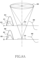
- FIG. 8A is a diagram illustrating changes of a luminance ratio obtained according to a change of a focus position of an image sensor 310 according to an embodiment.
- FIG. 8A may be described with reference to the configurations of the camera module 300 of FIG. 3 .
- luminance values of one column (or one row) of the image acquired by the image sensor 310 may correspond to a curve 810.
- luminance values of one column (or one row) of the images acquired by the first sub PDs of the image sensor 310 may correspond to a curve 811.
- luminance values of one column (or one row) of the images acquired by the second sub PDs of the image sensor 310 may correspond to a curve 815.
- the curve 810 may correspond to a sum of the curve 811 and the curve 815.
- a luminance ratio 820 may have relatively considerable changes in a form which is open to both sides as shown in the curve 811 and the curve 815.
- luminance values of one column (or one row) of the image acquired by the image sensor 310 may correspond to a curve 830.
- luminance values of one column (or one row) of the images acquired by the first sub PDs of the image sensor 310 may correspond to a curve 831.
- luminance values of one column (or one row) of the images acquired by the second sub PDs of the image sensor 310 may correspond to a curve 835.
- the curve 830 may correspond to a sum of the curve 831 and the curve 835.
- a luminance ratio 820 may have relatively small changes in a form converging to the center as shown in the curve 831 and the curve 835.
- positions of peak values of the curves 810 and 830 are similar to each other, whereas positions of peak values of the curves 811, 815, 831, and 835 may vary, according to the position of the image sensor 310.
- the luminance ratio may differ, depending on the optical characteristics (e.g., the position of the image sensor 310) of the image acquisition.
- FIG. 8B is a graph illustrating a luminance ratio of an image acquired at a first focus position of the image sensor 310 and an initial reference luminance ratio arbitrarily set according to an embodiment.
- FIG. 8C is a graph illustrating the luminance ratio of the image acquired at the first focus position of the image sensor 310 and the most similar reference luminance ratio according to an embodiment.
- a luminance ratio 855 of FIG. 8B and a luminance ratio 865 of FIG. 8C may be the same luminance ratios.
- FIG. 8D is a graph illustrating a luminance ratio of the image acquired at the second focus position of the image sensor 310 and the initial reference luminance ratio arbitrarily set according to an embodiment.
- FIG. 8E is a graph illustrating the luminance ratio of the image acquired at the second focus position of the image sensor 310 and the most similar reference luminance ratio according to an embodiment.
- a luminance ratio 875 of FIG. 8D and a luminance ratio 885 of FIG. 8E may be the same luminance ratios.
- FIG. 8B through FIG. 8E may be described with reference to the configurations of the camera module 300 of FIG. 3 .
- the matching unit 390 may identify the reference luminance ratio, by comparing the reference luminance ratios stored in the memory 395 with the luminance ratio 855 of the image acquired at the first focus position (e.g., the position of Z1, the position 850 of the near focus).
- a difference may exist between the luminance ratio 855 of the image acquired at the first focus position (e.g., the position of Z1, the position 850 of the near focus) and an initial reference luminance ratio 851 arbitrarily set.
- the matching unit 390 may not determine the arbitrarily set initial reference luminance ratio 851 as the reference luminance ratio for the luminance ratio 855 of the acquired image.
- the difference between the luminance ratio 865 of the image acquired at the first focus position (e.g., the position of Z1, the position of the near focus) and the reference luminance ratio 861 may be relatively less than other reference luminance ratios.
- the matching unit 390 may determine the reference luminance ratio 861 as the reference luminance ratio for the luminance ratio 865 of the acquired image.
- the matching unit 390 may not determine the arbitrarily set initial reference luminance ratio 871 as the reference luminance ratio for the luminance ratio 875 of the acquired image.
- the difference between the luminance ratio 885 of the image acquired at the second focus position (e.g., the position of Z2, the position of the far focus) and a reference luminance ratio 881 may be relatively less than other reference luminance ratios.
- the matching unit 390 may determine the reference luminance ratio 881 as the reference luminance ratio for the luminance ratio 885 of the acquired image.
- FIG. 9 is a block diagram illustrating a detection unit 355 and an image correction unit 350 of a camera module 300 according to an embodiment. FIG. 9 may be described with reference to the configurations of the camera module 300 of FIG. 3 .
- the detection unit 355 may include a foreign substance detection unit 910.
- the image correction unit 350 may include a shading correction unit 920.
- the foreign substance detection unit 910 may detect a defect (or, noise) due to a foreign substance in the raw image 701, based on the difference value ⁇ SR(i). In an embodiment, the foreign substance detection unit 910 may detect the defect (or, noise) caused by the foreign substance in the raw image 701, based on the average value of the difference value ⁇ SR(i). In an embodiment, if the average value of the difference value ⁇ SR(i) is greater than a predesignated reference average value, the foreign substance detection unit 910 may determine the defect (or, noise) due to the foreign substance in the raw image 701.
- the foreign substance detection unit 910 may provide information to the processor 120, to notify a notification to the user. In an embodiment, if determining the defect (or, noise) due to the foreign substance, the foreign substance detection unit 910 may provide information to the shading correction unit 920 to correct the defect (or, noise) due to the foreign substance.
- the shading correction unit 920 may identify a correction value which minimizes the difference value ⁇ SR(i), and correct the raw image 701, based on the identified correction value.
- FIG. 10A is a diagram illustrating an image 1010 acquired if there is no foreign substance on a cover of a camera module 300 according to an embodiment.
- FIG. 10B is a diagram illustrating an image 1020 acquired if there is a foreign substance 1025 on the cover of the camera module 300 according to an embodiment.
- FIG. 10C is a diagram illustrating light amount simulation results of the image acquired if there is no foreign substance on the cover of the camera module 300 according to an embodiment.
- FIG. 10D is a diagram illustrating light amount simulation results of the image acquired if there is the foreign substance on the cover of the camera module 300 according to an embodiment.
- FIG. 10A is a diagram illustrating an image 1010 acquired if there is no foreign substance on a cover of a camera module 300 according to an embodiment.
- FIG. 10B is a diagram illustrating an image 1020 acquired if there is a foreign substance 1025 on the cover of the camera module 300 according to an embodiment.
- FIG. 10C is a diagram illustrating light amount simulation results of the
- FIG. 10E is a graph illustrating a luminance ratio of the image acquired if there is the foreign substance on the cover of the camera module 300 and a reference luminance ratio according to an embodiment.
- FIG. 10A through FIG. 10E may be described with reference to the configurations of the camera module 300 of FIG. 3 .
- a difference between the images 1010 and 1020 may not be visually recognized.
- a difference of the light amount may occur between the images 1010 and 1020 according to a type of the foreign substance and/or a shape of the foreign substance. Referring to FIG. 10D , the light amount is reduced, in a region 1045 having the foreign substance, compared to the absence of the foreign substance of FIG. 10C .
- a luminance ratio 1055 of the acquired raw image may be slightly different from a reference luminance ratio 1051.
- the shading correction unit 920 may identify a correction value for minimizing the difference value ⁇ SR(i) between the luminance ratio 1055 and the reference luminance ratio 1051, and correct the raw image, based on the identified correction value.
- FIG. 11 is a block diagram illustrating a detection unit 355 and an image correction unit 350 of a camera module 300 according to an embodiment.
- FIG. 11 may be described with reference to the configurations of the camera module 300 of FIG. 3 .
- the detection unit 355 may include a flare detection unit 1110.
- the image correction unit 350 may include a peeling unit 1120.
- the flare detection unit 1110 may detect a defect (or, noise) due to a flare in the raw image 701, based on the difference value ⁇ SR(i). In an embodiment, the flare detection unit 1110 may detect the defect (or, noise) due to the flare in the raw image 701, based on the difference value ⁇ SR(i) and the predesignated reference difference value. In an embodiment, the flare detection unit 1110 may determine a pixel having the difference value ⁇ SR(i) greater than the predesignated reference difference value among the pixels of the raw image 701 as a pixel having the defect (or, noise) due to the flare.
- the flare detection unit 1110 may provide information to the peeling unit 1120 to correct the defect (or, noise) due to the flare.
- the peeling unit 1120 may determine a value of the pixel having the defect (or, noise) due to the flare, based on values of pixels around the pixel having the defect (or, noise) due to the flare. In an embodiment, the peeling unit 1120 may correct the value of the pixel having the defect (or, noise) due to the flare, based on values of high-reliability pixels among the pixels around the pixel having the defect (or, noise) due to the flare.
- FIG. 12A is a diagram illustrating an image 1210 having a defect due to a flare.
- FIG. 12B is a graph illustrating a luminance ratio 1231 of the image 1210 having the defect due to the flare and a reference luminance ratio 1237.
- FIG. 12C is a diagram illustrating an image 1240 with the defect due to the flare corrected.
- FIG. 12A through FIG. 12C may be described with reference to the configurations of the camera module 300 of FIG. 3 .
- the image 1210 may be subject to light splitting 1213, light scattering 1215, or a combination thereof from the light source 1211. In an embodiment, if the light amount of the light source 1211 is high, a ghost phenomenon may occur in the image 1210.
- a luminance ratio 1231 of the pixel having the defect due to the flare among the pixels of the image 1210 may have more sharp points than a reference luminance ratio 1237.
- the image correction unit 350 e.g., the peeling unit 1120
- the image correction unit 350 may correct the pixel having the defect (or, noise) due to the flare based on high-reliability pixels with reference to the reference luminance ratio 1237.
- the image 1240 corrected the defect due to the flare is reduced in the size of the light source 1241, is reduced in the size of the light splitting 1243, and is reduced in the light scattering 1245, compared to the image 1210.
- FIG. 13 is a block diagram illustrating a detection unit 355 and an application 146 of a camera module 300 according to an embodiment.
- FIG. 13 may be described with reference to the configurations of the camera module 300 of FIG. 3 .
- the detection unit 355 may include a saturation detection unit 1310.
- the application 146 may include an exposure correction module 1320, an effect application module 1330, or a combination thereof.
- the saturation detection unit 1310 may detect a defect (or, noise) due to saturation in the raw image 701, based on the difference value ⁇ SR(i). In an embodiment, the saturation detection unit 1310 may identify a saturation level of the pixel having the corresponding difference value ⁇ SR(i) depending on which one of the value of 0, the value between 0 and the value obtained by subtracting the reference luminance ratio from 1, or the value obtained by subtracting the reference luminance ratio from 1 the difference value ⁇ SR(i) corresponds to.
- the saturation detection unit 1310 may provide information to the application 146, to correct an image effect.
- the exposure correction module 1320 of the application 146 may adjust exposure, focus, white balance, or a combination thereof, based on the saturation level. In an embodiment, the exposure correction module 1320 may adjust the exposure, the focus, the white balance, or a combination thereof, based on the saturation level, to avoid the saturation.
- the effect application module 1330 of the application 146 may control whether to apply the effect, based on the saturation level. In an embodiment, the effect application module 1330 of the application 146 may control not to apply a light source effect (e.g., a light splitting effect), to a portion having a low saturation level in the image. In an embodiment, the effect application module 1330 of the application 146 may control to apply the light source effect (e.g., a light splitting effect), to a portion of a high saturation level in the image. In an embodiment, the portion having the high saturation level in the image may be a portion corresponding to a pixel in which at least one sub PD of the sub PDs is saturated. In an embodiment, the portion having the low saturation level in the image may be a portion corresponding to a pixel in which the sub PD of the sub PDs is not saturated.
- a light source effect e.g., a light splitting effect
- the portion having the high saturation level in the image may be a portion corresponding to a pixel in
- FIG. 14A is a diagram illustrating an image 1410 having a low light amount.
- FIG. 14B is a diagram illustrating an image 1420 having a high light amount.
- FIG. 14C is a graph illustrating a signal value based on a saturation level.
- FIG. 14D is a graph illustrating a luminance ratio of the image 1410 having the low light amount.
- FIG. 14E is a graph illustrating a luminance ratio of the image 1420 having the high light amount.
- FIG. 14A through FIG. 14E shall be described with reference to the configurations of the camera module 300 of FIG. 3 .
- brightness of the light source 1411 of the image 1410 if the light amount is low and the light source 1421 of the image 1420 if the light amount is high may be identical due to the saturation.
- a sum signal 1431 of a signal 1433 by the first PD 415L and a signal 1435 by the second PD 415R may be the same as the actual signal.
- a sum signal 1441 of the signal 1443 by the first PD 415L and the signal 1445 by the second PD 415R may be different from the actual signal 1442. This is because the signal 1444 corresponding to the light amount actually applied to the first PD 415L is not outputted due to the saturation of the first PD 415L.
- a sum signal 1451 of a signal 1453 by the first PD 415L and a signal 1455 by the second PD 415R may be different from an actual signal 1452. This is because the signal 1454 corresponding to the light amount actually applied to the first PD 415L is not outputted due to the saturation of the first PD 415L, and the signal 1456 corresponding to the light amount actually applied to the second PD 415R is not outputted due to the saturation of the first PD 415L
- part of the luminance ratio of the image 1410 if the light amount is low and part of the luminance ratio of the image 1420 if the light amount is high may indicate the saturation.
- the exposure correction module 1320 may adjust the exposure, the focus, the white balance, or a combination thereof, based on the saturation level.
- the effect application module 1330 may control whether to apply the effect, based on the saturation level.
- FIG. 15 is a diagram illustrating an image 1510 to which a light source effect is applied differently according to a saturation level.
- the light splitting effect is not applied to a light source 1520 having a low saturation level, and the light splitting effect is applied to light sources 1530 and 1540 having high saturation levels.
- FIG. 16 is a flowchart illustrating operations of an electronic device (e.g., the electronic device 101) according to an embodiment.
- FIG. 16 shall be described with reference to the configurations of the camera module 300 of FIG. 3 .
- the camera module 300 of the electronic device 101 may detect light through multiple PDs (e.g., the PDs 410). In an embodiment, the camera module 300 may detect the light through each of the plurality of the PDs 410 of the image sensor 310.
- the camera module 300 may detect a luminance ratio of at least two sub images corresponding to the detected light.
- the luminance ratio may be a ratio between luminance values of pixels at corresponding positions in the sub images.
- the camera module 300 may detect a luminance ratio between a first sub image corresponding to light detected by a first sub PD (e.g., the first sub PD 415L) of the multi-PD and a second sub image corresponding to light detected by a second sub PD (e.g., the second sub PD 415R) of the multi-PD.
- the at least two sub images may be luminance images.
- the camera module 300 may detect an image region based on the detected luminance ratio.
- the camera module 300 may detect the image region having a defect (or, noise) based on the detected luminance ratio.
- the defect may include a foreign substance, a flare, saturation, or a combination thereof.
- the camera module 300 may correct the detected image region.
- the camera module 300 may correct the value of each of the pixels of the raw image 701, based on information of at least one defect (or, noise).
- the camera module 300 may correct values of pixels of the first raw sub image and the second raw sub image, based on the information of at least one defect (or, noise).
- the camera module 300 may correct the values of the pixels of the raw image 701, based on a correction value corresponding to the luminance ratio of each of the pixels of the raw image 701. In an embodiment, if the raw image 701 has a defect (or, noise) due to a flare, the camera module 300 may correct a value of a pixel having the defect (or, noise) due to the flare, based on values of pixels around the pixel having the defect (or, noise) due to the flare.
- An electronic device may include a memory, an image sensor in which light receiving elements are arranged, the light receiving elements each including at least two sub light receiving elements, and an image signal processor operatively coupled with the memory, and the image sensor, and the image signal processor may be configured to obtain images corresponding to light from outside by using the image sensor, the images including at least a raw image, a first sub image, and a second sub image, the first sub image being an image corresponding to light sensed by at least one first sub light receiving element positioned at a first position corresponding in the light receiving elements, the second sub image being an image corresponding to light sensed by at least one second sub light receiving element positioned at a second position corresponding in the light receiving elements, the first position distinguished from the second position, identify a luminance ratio between the first sub image and the second sub image, identify a defect in the raw image, based on the identified luminance ratio, and perform a function corresponding to a type of the identified defect.
- the type of the defect may include a foreign substance, a flare, saturation, or a combination thereof.
- the image signal processor may be configured to identify the foreign substance in the raw image, based on an average value of a difference value obtained by subtracting a reference luminance ratio from the luminance ratio.
- the image signal processor may be configured to, if identifying the foreign substance, identify a correction value for the raw image, based on the identified luminance ratio, and correct the raw image based on the identified correction value.
- the image signal processor may be configured to identify the flare in the raw image, based on a difference value obtained by subtracting a reference luminance ratio from the luminance ratio.
- the image signal processor may be configured to identify a first pixel of which the difference value exceeds a predesignated reference value as a pixel indicating the flare among pixels of the raw image, and correct the raw image, by correcting a value of the first pixel, based on values of adj acent pixels of the first pixel among the pixels of the raw image.
- the image signal processor may be configured to correct the raw image, by correcting the value of the first pixel, based on values of adjacent pixels having reliability greater than or equal to predesignated reliability among adjacent pixels of the first pixel.
- the image signal processor may be configured to identify the saturation in the raw image, based on a position at which the luminance ratio is positioned in an interval between a reference luminance ratio and a predesignated reference value.
- the image signal processor may be configured to, if the luminance ratio is positioned in the interval between the reference luminance ratio and the predesignated reference value, identify that one sub light receiving element of the at least two sub light receiving elements of the first light receiving element used to obtain the ratio among the light receiving elements is saturated, and estimate a value of a pixel corresponding to the first light receiving element among pixels of the raw image, based on an output value of an unsaturated sub light receiving element among the at least two sub light receiving elements of the first light receiving element.
- the image signal processor may be configured to, if the saturation is identified, control an exposure degree of the image sensor, auto white balance (AWB), or a combination thereof.
- AVB auto white balance
- An operating method of an electronic device may include obtaining images corresponding to light from outside by using an image sensor of the electronic device, the images including at least a raw image, a first sub image, and a second sub image, the first sub image being an image corresponding to light sensed by at least one first sub light receiving element positioned at a first position corresponding in the light receiving elements of the electronic device, the second sub image being an image corresponding to light sensed by at least one second sub light receiving element positioned at a second position corresponding in the light receiving elements, the first position distinguished from the second position, identifying a luminance ratio between the first sub image and the second sub image, identifying a defect in the raw image, based on the identified luminance ratio, and performing a function corresponding to a type of the identified defect.
- the type of the defect may include a foreign substance, a flare, saturation, or a combination thereof.
- identifying the defect in the raw image may include identifying the foreign substance in the raw image, based on an average value of a difference value obtained by subtracting a reference luminance ratio from the luminance ratio.
- performing the function corresponding to the type of the identified defect may include, if identifying the foreign substance, identifying a correction value for the raw image, based on the identified luminance ratio, and correcting the raw image based on the identified correction value.
- identifying the defect in the raw image may include identifying the flare in the raw image, based on a difference value obtained by subtracting a reference luminance ratio from the luminance ratio.
- performing the function corresponding to the type of the identified defect may include identifying a first pixel of which the difference value exceeds a predesignated reference value as a pixel indicating the flare among pixels of the raw image, and correcting the raw image, by correcting a value of the first pixel, based on values of adjacent pixels of the first pixel among the pixels of the raw image.
- correcting the raw image may include correcting the raw image, by correcting the value of the first pixel, based on values of adjacent pixels having reliability greater than or equal to predesignated reliability among adjacent pixels of the first pixel.
- identifying the defect in the raw image may include identifying the saturation in the raw image, based on a position at which the luminance ratio is positioned in an interval between a reference luminance ratio and a predesignated reference value.
- identifying the defect in the raw image may include, if the luminance ratio is positioned in the interval between the reference luminance ratio and the predesignated reference value, identifying that one sub light receiving element of the at least two sub light receiving elements of the first light receiving element used to obtain the ratio among the light receiving elements is saturated, and estimating a value of a pixel corresponding to the first light receiving element among pixels of the raw image, based on an output value of an unsaturated sub light receiving element among the at least two sub light receiving elements of the first light receiving element.
- performing the function corresponding to the type of the identified defect may include, if the saturation is identified, control an exposure degree of the image sensor, AWB, or a combination thereof.
- a computer-readable storage medium storing one or more programs (software modules) may be provided.
- One or more programs stored in the computer-readable storage medium may be configured for execution by one or more processors of an electronic device.
- One or more programs may include instructions for controlling an electronic device to execute the methods according to the embodiments described in the claims or the specification of the present disclosure.
- Such a program may be stored to a random access memory, a non-volatile memory including a flash memory, a read only memory (ROM), an electrically erasable programmable ROM (EEPROM), a magnetic disc storage device, a compact disc (CD)-ROM, digital versatile discs (DVDs) or other optical storage devices, and a magnetic cassette. Alternatively, it may be stored to a memory combining part or all of those recording media. A plurality of memories may be included.
- the program may be stored in an attachable storage device accessible via a communication network such as internet, intranet, local area network (LAN), wide LAN (WLAN), or storage area network (SAN), or a communication network by combining these networks.
- a storage device may access a device which executes an embodiment of the present disclosure through an external port.
- a separate storage device on the communication network may access the device which executes an embodiment of the present disclosure.
- the components included in the present disclosure are expressed in a singular or plural form.
- the singular or plural expression is appropriately selected according to a proposed situation for the convenience of explanation, the present disclosure is not limited to a single component or a plurality of components, the components expressed in the plural form may be configured as a single component, and the components expressed in the singular form may be configured as a plurality of components.
Landscapes
- Engineering & Computer Science (AREA)
- Theoretical Computer Science (AREA)
- General Physics & Mathematics (AREA)
- Physics & Mathematics (AREA)
- Multimedia (AREA)
- Computer Vision & Pattern Recognition (AREA)
- Software Systems (AREA)
- Signal Processing (AREA)
- Databases & Information Systems (AREA)
- Health & Medical Sciences (AREA)
- Artificial Intelligence (AREA)
- Computing Systems (AREA)
- Evolutionary Computation (AREA)
- General Health & Medical Sciences (AREA)
- Medical Informatics (AREA)
- Quality & Reliability (AREA)
- Studio Devices (AREA)
Applications Claiming Priority (2)
| Application Number | Priority Date | Filing Date | Title |
|---|---|---|---|
| KR1020200046911A KR20210128803A (ko) | 2020-04-17 | 2020-04-17 | 다중 포토다이오드 센서에 의해 획득된 서브 이미지들의 차이에 기반하여 이미지의 결함을 검출하는 전자 장치 및 이의 동작 방법 |
| PCT/KR2021/004608 WO2021210875A1 (fr) | 2020-04-17 | 2021-04-13 | Dispositif électronique permettant de détecter un défaut dans une image sur la base d'une différence entre des sous-images acquises par un capteur à photodiodes multiples, et son procédé de fonctionnement |
Publications (3)
| Publication Number | Publication Date |
|---|---|
| EP4138034A1 true EP4138034A1 (fr) | 2023-02-22 |
| EP4138034A4 EP4138034A4 (fr) | 2023-06-14 |
| EP4138034B1 EP4138034B1 (fr) | 2025-02-26 |
Family
ID=78084291
Family Applications (1)
| Application Number | Title | Priority Date | Filing Date |
|---|---|---|---|
| EP21788871.8A Active EP4138034B1 (fr) | 2020-04-17 | 2021-04-13 | Dispositif électronique permettant de détecter un défaut dans une image sur la base d'une différence entre des sous-images acquises par un capteur à photodiodes multiples, et son procédé de fonctionnement |
Country Status (4)
| Country | Link |
|---|---|
| US (1) | US12333696B2 (fr) |
| EP (1) | EP4138034B1 (fr) |
| KR (1) | KR20210128803A (fr) |
| WO (1) | WO2021210875A1 (fr) |
Families Citing this family (4)
| Publication number | Priority date | Publication date | Assignee | Title |
|---|---|---|---|---|
| US12614370B2 (en) * | 2021-09-17 | 2026-04-28 | Hewlett-Packard Development Company, L.P. | Exposures for areas of image sensors |
| EP4492810A4 (fr) * | 2022-05-27 | 2025-06-04 | Samsung Electronics Co., Ltd | Dispositif électronique comprenant un module de caméra et son procédé de commande |
| WO2023229435A1 (fr) * | 2022-05-27 | 2023-11-30 | 삼성전자 주식회사 | Dispositif électronique comprenant un module de caméra et son procédé de commande |
| US12311502B1 (en) | 2024-08-02 | 2025-05-27 | Communications Test Design, Inc. | Electronic device screen polishing apparatus and method for the same |
Family Cites Families (41)
| Publication number | Priority date | Publication date | Assignee | Title |
|---|---|---|---|---|
| EP1528797B1 (fr) | 2003-10-31 | 2015-07-08 | Canon Kabushiki Kaisha | Appareil de traitement d'image, sytème d'acquisition d'image et procédé de traitement d'image |
| JP4774915B2 (ja) * | 2005-10-26 | 2011-09-21 | カシオ計算機株式会社 | 撮像装置、階調補正方法及びプログラム |
| US7639369B2 (en) | 2006-04-13 | 2009-12-29 | Mette Owner-Petersen | Multi-object wavefront sensor with spatial filtering |
| US8208043B2 (en) | 2008-05-09 | 2012-06-26 | Aptina Imaging Corporation | Lens cleaning warning system and method |
| EP2287807A1 (fr) * | 2009-07-21 | 2011-02-23 | Nikon Corporation | Dispositif de traitement d'image, programme de traitement d'image et dispositif d'imagerie. |
| US8279349B2 (en) * | 2009-11-17 | 2012-10-02 | Nice Systems Ltd. | Automatic control of visual parameters in video processing |
| US9020281B2 (en) | 2010-03-01 | 2015-04-28 | Konika Minolta Advanced Layers, Inc. | Ghost detection device and imaging device using the same, ghost detection method and ghost removal method |
| JP5699621B2 (ja) * | 2011-01-19 | 2015-04-15 | 株式会社リコー | 画像処理装置、画素補間方法およびプログラム |
| US20150241350A1 (en) | 2011-08-26 | 2015-08-27 | Edward J. Miesak | Latent fingerprint detection |
| KR101946946B1 (ko) | 2012-08-08 | 2019-04-25 | 엘지이노텍 주식회사 | 이미지 처리 장치 및 이의 이미지 처리 방법 |
| JP6185249B2 (ja) | 2012-04-27 | 2017-08-23 | エルジー イノテック カンパニー リミテッド | イメージ処理装置及びイメージ処理方法 |
| JP5657182B2 (ja) * | 2012-05-10 | 2015-01-21 | 富士フイルム株式会社 | 撮像装置及び信号補正方法 |
| WO2014017626A1 (fr) | 2012-07-27 | 2014-01-30 | 日産自動車株式会社 | Dispositif de caméra, dispositif de détection d'objet tridimensionnel et procédé de nettoyage de lentille |
| JP6021613B2 (ja) * | 2012-11-29 | 2016-11-09 | キヤノン株式会社 | 撮像素子、撮像装置、および、撮像システム |
| US9445057B2 (en) | 2013-02-20 | 2016-09-13 | Magna Electronics Inc. | Vehicle vision system with dirt detection |
| US9497427B2 (en) | 2013-07-15 | 2016-11-15 | Semiconductor Components Industries, Llc | Method and apparatus for image flare mitigation |
| JP6245875B2 (ja) | 2013-07-26 | 2017-12-13 | クラリオン株式会社 | レンズ汚れ検出装置およびレンズ汚れ検出方法 |
| CN106415598B (zh) | 2014-05-27 | 2020-08-28 | 罗伯特·博世有限公司 | 用于车载式相机系统的镜头污染的检测、识别和缓解 |
| EP3164831A4 (fr) * | 2014-07-04 | 2018-02-14 | Light Labs Inc. | Procédés et appareils se rapportant à la détection et/ou l'indication d'un état de lentille sale |
| JP2016033729A (ja) | 2014-07-31 | 2016-03-10 | クラリオン株式会社 | 周囲環境認識装置 |
| US9749556B2 (en) * | 2015-03-24 | 2017-08-29 | Semiconductor Components Industries, Llc | Imaging systems having image sensor pixel arrays with phase detection capabilities |
| JP2016225932A (ja) * | 2015-06-03 | 2016-12-28 | セイコーエプソン株式会社 | 搬送装置、印刷装置及び搬送情報取得方法 |
| EP3113108B1 (fr) | 2015-07-02 | 2020-03-11 | Continental Automotive GmbH | Détection de contamination de lentille au moyen de trajectoires de bord attendues |
| US9979909B2 (en) | 2015-07-24 | 2018-05-22 | Lytro, Inc. | Automatic lens flare detection and correction for light-field images |
| US10298863B2 (en) | 2015-09-08 | 2019-05-21 | Apple Inc. | Automatic compensation of lens flare |
| US10225445B2 (en) | 2015-12-18 | 2019-03-05 | Light Labs Inc. | Methods and apparatus for providing a camera lens or viewing point indicator |
| US10402696B2 (en) | 2016-01-04 | 2019-09-03 | Texas Instruments Incorporated | Scene obstruction detection using high pass filters |
| JP6638453B2 (ja) * | 2016-02-16 | 2020-01-29 | コニカミノルタ株式会社 | 不良画像発生予測システム及び不良画像発生予測プログラム |
| US9838594B2 (en) * | 2016-03-02 | 2017-12-05 | Qualcomm Incorporated | Irregular-region based automatic image correction |
| JP6757184B2 (ja) | 2016-03-24 | 2020-09-16 | キヤノン株式会社 | 画像処理装置、撮像装置およびこれらの制御方法ならびにプログラム |
| KR102688619B1 (ko) | 2016-09-30 | 2024-07-26 | 삼성전자주식회사 | 이미지 처리 방법 및 이를 지원하는 전자 장치 |
| JP2018106456A (ja) * | 2016-12-27 | 2018-07-05 | セイコーエプソン株式会社 | 画像処理装置、および、画像処理方法 |
| JP6932947B2 (ja) * | 2017-03-02 | 2021-09-08 | コニカミノルタ株式会社 | 不良画像発生予測システム及び不良画像発生予測プログラム |
| US10623640B2 (en) | 2017-03-17 | 2020-04-14 | Uurmi Systems Pvt Ltd | Method and system for detection of contaminants present on a lens of an imaging device |
| JP6941011B2 (ja) * | 2017-09-04 | 2021-09-29 | キヤノン株式会社 | 撮像装置及びその制御方法、プログラム、記憶媒体 |
| JP7003502B2 (ja) | 2017-09-04 | 2022-01-20 | 株式会社アイシン | 検査装置 |
| JP2018013794A (ja) * | 2017-09-07 | 2018-01-25 | 株式会社ニコン | 撮像装置 |
| JP6643301B2 (ja) * | 2017-12-06 | 2020-02-12 | 日東電工株式会社 | 欠陥検査装置及び欠陥検査方法 |
| JP7030562B2 (ja) * | 2018-02-28 | 2022-03-07 | キヤノン株式会社 | 画像処理装置、画像処理方法及びプログラム |
| CN120339355A (zh) | 2018-09-18 | 2025-07-18 | 松下知识产权经营株式会社 | 信息处理方法、信息处理装置以及计算机程序产品 |
| JP6961558B2 (ja) | 2018-10-05 | 2021-11-05 | 株式会社キトー | 電気チェーンブロックおよびこれに用いられるバネガイド |
-
2020
- 2020-04-17 KR KR1020200046911A patent/KR20210128803A/ko active Pending
-
2021
- 2021-04-13 WO PCT/KR2021/004608 patent/WO2021210875A1/fr not_active Ceased
- 2021-04-13 EP EP21788871.8A patent/EP4138034B1/fr active Active
-
2022
- 2022-10-11 US US17/963,664 patent/US12333696B2/en active Active
Also Published As
| Publication number | Publication date |
|---|---|
| WO2021210875A1 (fr) | 2021-10-21 |
| EP4138034A4 (fr) | 2023-06-14 |
| EP4138034B1 (fr) | 2025-02-26 |
| US12333696B2 (en) | 2025-06-17 |
| US20230042544A1 (en) | 2023-02-09 |
| KR20210128803A (ko) | 2021-10-27 |
Similar Documents
| Publication | Publication Date | Title |
|---|---|---|
| US11461910B2 (en) | Electronic device for blurring image obtained by combining plural images based on depth information and method for driving the electronic device | |
| US12333696B2 (en) | Electronic device for detecting defect in image on basis of difference among sub-images acquired by multiple photodiode sensors, and operation method thereof | |
| US11363199B2 (en) | Apparatus and method for estimating optical image stabilization motion | |
| US10785409B2 (en) | Electronic device combining plurality of images based on image brightness and method therefor | |
| EP3815356B1 (fr) | Dispositif électronique et procédé d'acquisition d'informations de profondeur à l'aide au moins de caméras ou d'un capteur de profondeur | |
| US20230209202A1 (en) | Electronic device for performing image stabilization, and operating method therefor | |
| KR102407200B1 (ko) | 하나의 이미지 센서를 통해 획득된 rgb 이미지와 ir 이미지를 이용하여 기능을 제공하는 전자 장치 | |
| US11354777B2 (en) | Image processing device and method of electronic device | |
| EP4329286A1 (fr) | Dispositif électronique pour synchroniser des informations de commande de lentille avec une image | |
| US12069382B2 (en) | Electronic device and method for generating images by performing auto white balance | |
| US12501171B2 (en) | Image capturing method and electronic device for capturing images using different light emissions | |
| CN116325777A (zh) | 获取光量的电子设备及方法 | |
| US20230267702A1 (en) | Electronic device including camera module and method for operating electronic device | |
| US12348865B2 (en) | Electronic device, and method for performing autofocus by rotating or reordering AF data | |
| US11032462B2 (en) | Method for adjusting focus based on spread-level of display object and electronic device supporting the same | |
| KR20220159133A (ko) | 촬영 시 흔들림을 보정하는 방법 및 그 전자 장치 | |
| US12335638B2 (en) | Electronic device comprising image sensor and operation method of same | |
| US12081861B2 (en) | Method for providing image and electronic device supporting the same | |
| US12177575B2 (en) | Photographing method of electronic apparatus and electronic apparatus thereof | |
| KR20210114768A (ko) | 서브 이미지들의 차이에 기반하여 이미지의 렌즈 쉐이딩을 보정하는 전자 장치 및 이의 동작 방법 | |
| KR20220153366A (ko) | 이미지 왜곡을 보정하는 방법 및 그 전자 장치 | |
| US20250175709A1 (en) | Electronic device for generating image and operating method thereof | |
| US11843874B2 (en) | Electronic device including under display camera and operating method thereof | |
| EP4307702A1 (fr) | Dispositif électronique comprenant un capteur d'image et procédé de fonctionnement associé | |
| EP4228246A1 (fr) | Dispositif électronique apte à réaliser une mise au point automatique et son procédé de fonctionnement |
Legal Events
| Date | Code | Title | Description |
|---|---|---|---|
| STAA | Information on the status of an ep patent application or granted ep patent |
Free format text: STATUS: THE INTERNATIONAL PUBLICATION HAS BEEN MADE |
|
| PUAI | Public reference made under article 153(3) epc to a published international application that has entered the european phase |
Free format text: ORIGINAL CODE: 0009012 |
|
| STAA | Information on the status of an ep patent application or granted ep patent |
Free format text: STATUS: REQUEST FOR EXAMINATION WAS MADE |
|
| 17P | Request for examination filed |
Effective date: 20221116 |
|
| AK | Designated contracting states |
Kind code of ref document: A1 Designated state(s): AL AT BE BG CH CY CZ DE DK EE ES FI FR GB GR HR HU IE IS IT LI LT LU LV MC MK MT NL NO PL PT RO RS SE SI SK SM TR |
|
| REG | Reference to a national code |
Ref country code: DE Ref legal event code: R079 Free format text: PREVIOUS MAIN CLASS: G06T0007000000 Ipc: G06V0010141000 Ref document number: 602021026849 Country of ref document: DE |
|
| A4 | Supplementary search report drawn up and despatched |
Effective date: 20230517 |
|
| RIC1 | Information provided on ipc code assigned before grant |
Ipc: H04N 25/704 20230101ALI20230511BHEP Ipc: H04N 25/61 20230101ALI20230511BHEP Ipc: H04N 25/683 20230101ALI20230511BHEP Ipc: H04N 23/82 20230101ALI20230511BHEP Ipc: H04N 23/81 20230101ALI20230511BHEP Ipc: G06T 5/00 20060101ALI20230511BHEP Ipc: G06T 5/50 20060101ALI20230511BHEP Ipc: G06T 7/00 20170101ALI20230511BHEP Ipc: G06V 10/74 20220101ALI20230511BHEP Ipc: G06V 10/75 20220101ALI20230511BHEP Ipc: G06V 10/60 20220101ALI20230511BHEP Ipc: G06V 10/141 20220101AFI20230511BHEP |
|
| DAV | Request for validation of the european patent (deleted) | ||
| DAX | Request for extension of the european patent (deleted) | ||
| STAA | Information on the status of an ep patent application or granted ep patent |
Free format text: STATUS: EXAMINATION IS IN PROGRESS |
|
| 17Q | First examination report despatched |
Effective date: 20240221 |
|
| GRAP | Despatch of communication of intention to grant a patent |
Free format text: ORIGINAL CODE: EPIDOSNIGR1 |
|
| STAA | Information on the status of an ep patent application or granted ep patent |
Free format text: STATUS: GRANT OF PATENT IS INTENDED |
|
| INTG | Intention to grant announced |
Effective date: 20241017 |
|
| RIN1 | Information on inventor provided before grant (corrected) |
Inventor name: JEONG, SANGHWAN Inventor name: YANG, HONGSEOK Inventor name: BAE, JAECHEOL Inventor name: KIM, CHANGGON Inventor name: KIM, EUNHO Inventor name: LEE, JEONGWON |
|
| GRAS | Grant fee paid |
Free format text: ORIGINAL CODE: EPIDOSNIGR3 |
|
| GRAA | (expected) grant |
Free format text: ORIGINAL CODE: 0009210 |
|
| STAA | Information on the status of an ep patent application or granted ep patent |
Free format text: STATUS: THE PATENT HAS BEEN GRANTED |
|
| AK | Designated contracting states |
Kind code of ref document: B1 Designated state(s): AL AT BE BG CH CY CZ DE DK EE ES FI FR GB GR HR HU IE IS IT LI LT LU LV MC MK MT NL NO PL PT RO RS SE SI SK SM TR |
|
| REG | Reference to a national code |
Ref country code: GB Ref legal event code: FG4D |
|
| REG | Reference to a national code |
Ref country code: CH Ref legal event code: EP |
|
| REG | Reference to a national code |
Ref country code: DE Ref legal event code: R096 Ref document number: 602021026849 Country of ref document: DE |
|
| REG | Reference to a national code |
Ref country code: IE Ref legal event code: FG4D |
|
| REG | Reference to a national code |
Ref country code: NL Ref legal event code: MP Effective date: 20250226 |
|
| PG25 | Lapsed in a contracting state [announced via postgrant information from national office to epo] |
Ref country code: RS Free format text: LAPSE BECAUSE OF FAILURE TO SUBMIT A TRANSLATION OF THE DESCRIPTION OR TO PAY THE FEE WITHIN THE PRESCRIBED TIME-LIMIT Effective date: 20250526 |
|
| PG25 | Lapsed in a contracting state [announced via postgrant information from national office to epo] |
Ref country code: FI Free format text: LAPSE BECAUSE OF FAILURE TO SUBMIT A TRANSLATION OF THE DESCRIPTION OR TO PAY THE FEE WITHIN THE PRESCRIBED TIME-LIMIT Effective date: 20250226 |
|
| PG25 | Lapsed in a contracting state [announced via postgrant information from national office to epo] |
Ref country code: PL Free format text: LAPSE BECAUSE OF FAILURE TO SUBMIT A TRANSLATION OF THE DESCRIPTION OR TO PAY THE FEE WITHIN THE PRESCRIBED TIME-LIMIT Effective date: 20250226 |
|
| PGFP | Annual fee paid to national office [announced via postgrant information from national office to epo] |
Ref country code: DE Payment date: 20250320 Year of fee payment: 5 |
|
| PG25 | Lapsed in a contracting state [announced via postgrant information from national office to epo] |
Ref country code: ES Free format text: LAPSE BECAUSE OF FAILURE TO SUBMIT A TRANSLATION OF THE DESCRIPTION OR TO PAY THE FEE WITHIN THE PRESCRIBED TIME-LIMIT Effective date: 20250226 |
|
| REG | Reference to a national code |
Ref country code: LT Ref legal event code: MG9D |
|
| PG25 | Lapsed in a contracting state [announced via postgrant information from national office to epo] |
Ref country code: IS Free format text: LAPSE BECAUSE OF FAILURE TO SUBMIT A TRANSLATION OF THE DESCRIPTION OR TO PAY THE FEE WITHIN THE PRESCRIBED TIME-LIMIT Effective date: 20250626 Ref country code: NO Free format text: LAPSE BECAUSE OF FAILURE TO SUBMIT A TRANSLATION OF THE DESCRIPTION OR TO PAY THE FEE WITHIN THE PRESCRIBED TIME-LIMIT Effective date: 20250526 |
|
| PG25 | Lapsed in a contracting state [announced via postgrant information from national office to epo] |
Ref country code: NL Free format text: LAPSE BECAUSE OF FAILURE TO SUBMIT A TRANSLATION OF THE DESCRIPTION OR TO PAY THE FEE WITHIN THE PRESCRIBED TIME-LIMIT Effective date: 20250226 |
|
| PG25 | Lapsed in a contracting state [announced via postgrant information from national office to epo] |
Ref country code: HR Free format text: LAPSE BECAUSE OF FAILURE TO SUBMIT A TRANSLATION OF THE DESCRIPTION OR TO PAY THE FEE WITHIN THE PRESCRIBED TIME-LIMIT Effective date: 20250226 |
|
| PG25 | Lapsed in a contracting state [announced via postgrant information from national office to epo] |
Ref country code: PT Free format text: LAPSE BECAUSE OF FAILURE TO SUBMIT A TRANSLATION OF THE DESCRIPTION OR TO PAY THE FEE WITHIN THE PRESCRIBED TIME-LIMIT Effective date: 20250626 Ref country code: LV Free format text: LAPSE BECAUSE OF FAILURE TO SUBMIT A TRANSLATION OF THE DESCRIPTION OR TO PAY THE FEE WITHIN THE PRESCRIBED TIME-LIMIT Effective date: 20250226 |
|
| PG25 | Lapsed in a contracting state [announced via postgrant information from national office to epo] |
Ref country code: BG Free format text: LAPSE BECAUSE OF FAILURE TO SUBMIT A TRANSLATION OF THE DESCRIPTION OR TO PAY THE FEE WITHIN THE PRESCRIBED TIME-LIMIT Effective date: 20250226 Ref country code: GR Free format text: LAPSE BECAUSE OF FAILURE TO SUBMIT A TRANSLATION OF THE DESCRIPTION OR TO PAY THE FEE WITHIN THE PRESCRIBED TIME-LIMIT Effective date: 20250527 |
|
| REG | Reference to a national code |
Ref country code: AT Ref legal event code: MK05 Ref document number: 1771440 Country of ref document: AT Kind code of ref document: T Effective date: 20250226 |
|
| PG25 | Lapsed in a contracting state [announced via postgrant information from national office to epo] |
Ref country code: SE Free format text: LAPSE BECAUSE OF FAILURE TO SUBMIT A TRANSLATION OF THE DESCRIPTION OR TO PAY THE FEE WITHIN THE PRESCRIBED TIME-LIMIT Effective date: 20250226 |
|
| PG25 | Lapsed in a contracting state [announced via postgrant information from national office to epo] |
Ref country code: SM Free format text: LAPSE BECAUSE OF FAILURE TO SUBMIT A TRANSLATION OF THE DESCRIPTION OR TO PAY THE FEE WITHIN THE PRESCRIBED TIME-LIMIT Effective date: 20250226 |
|
| PG25 | Lapsed in a contracting state [announced via postgrant information from national office to epo] |
Ref country code: DK Free format text: LAPSE BECAUSE OF FAILURE TO SUBMIT A TRANSLATION OF THE DESCRIPTION OR TO PAY THE FEE WITHIN THE PRESCRIBED TIME-LIMIT Effective date: 20250226 |
|
| PG25 | Lapsed in a contracting state [announced via postgrant information from national office to epo] |
Ref country code: IT Free format text: LAPSE BECAUSE OF FAILURE TO SUBMIT A TRANSLATION OF THE DESCRIPTION OR TO PAY THE FEE WITHIN THE PRESCRIBED TIME-LIMIT Effective date: 20250226 |
|
| PG25 | Lapsed in a contracting state [announced via postgrant information from national office to epo] |
Ref country code: AT Free format text: LAPSE BECAUSE OF FAILURE TO SUBMIT A TRANSLATION OF THE DESCRIPTION OR TO PAY THE FEE WITHIN THE PRESCRIBED TIME-LIMIT Effective date: 20250226 |
|
| PG25 | Lapsed in a contracting state [announced via postgrant information from national office to epo] |
Ref country code: EE Free format text: LAPSE BECAUSE OF FAILURE TO SUBMIT A TRANSLATION OF THE DESCRIPTION OR TO PAY THE FEE WITHIN THE PRESCRIBED TIME-LIMIT Effective date: 20250226 Ref country code: CZ Free format text: LAPSE BECAUSE OF FAILURE TO SUBMIT A TRANSLATION OF THE DESCRIPTION OR TO PAY THE FEE WITHIN THE PRESCRIBED TIME-LIMIT Effective date: 20250226 |
|
| PG25 | Lapsed in a contracting state [announced via postgrant information from national office to epo] |
Ref country code: RO Free format text: LAPSE BECAUSE OF FAILURE TO SUBMIT A TRANSLATION OF THE DESCRIPTION OR TO PAY THE FEE WITHIN THE PRESCRIBED TIME-LIMIT Effective date: 20250226 |
|
| PG25 | Lapsed in a contracting state [announced via postgrant information from national office to epo] |
Ref country code: SK Free format text: LAPSE BECAUSE OF FAILURE TO SUBMIT A TRANSLATION OF THE DESCRIPTION OR TO PAY THE FEE WITHIN THE PRESCRIBED TIME-LIMIT Effective date: 20250226 |
|
| REG | Reference to a national code |
Ref country code: CH Ref legal event code: H13 Free format text: ST27 STATUS EVENT CODE: U-0-0-H10-H13 (AS PROVIDED BY THE NATIONAL OFFICE) Effective date: 20251125 |
|
| REG | Reference to a national code |
Ref country code: DE Ref legal event code: R097 Ref document number: 602021026849 Country of ref document: DE |
|
| PG25 | Lapsed in a contracting state [announced via postgrant information from national office to epo] |
Ref country code: LU Free format text: LAPSE BECAUSE OF NON-PAYMENT OF DUE FEES Effective date: 20250413 |
|
| PG25 | Lapsed in a contracting state [announced via postgrant information from national office to epo] |
Ref country code: MC Free format text: LAPSE BECAUSE OF FAILURE TO SUBMIT A TRANSLATION OF THE DESCRIPTION OR TO PAY THE FEE WITHIN THE PRESCRIBED TIME-LIMIT Effective date: 20250226 |
|
| REG | Reference to a national code |
Ref country code: BE Ref legal event code: MM Effective date: 20250430 |
|
| PLBE | No opposition filed within time limit |
Free format text: ORIGINAL CODE: 0009261 |
|
| STAA | Information on the status of an ep patent application or granted ep patent |
Free format text: STATUS: NO OPPOSITION FILED WITHIN TIME LIMIT |
|
| PG25 | Lapsed in a contracting state [announced via postgrant information from national office to epo] |
Ref country code: FR Free format text: LAPSE BECAUSE OF NON-PAYMENT OF DUE FEES Effective date: 20250426 |
|
| PG25 | Lapsed in a contracting state [announced via postgrant information from national office to epo] |
Ref country code: BE Free format text: LAPSE BECAUSE OF NON-PAYMENT OF DUE FEES Effective date: 20250430 |
|
| PG25 | Lapsed in a contracting state [announced via postgrant information from national office to epo] |
Ref country code: CH Free format text: LAPSE BECAUSE OF NON-PAYMENT OF DUE FEES Effective date: 20250430 |
|
| GBPC | Gb: european patent ceased through non-payment of renewal fee |
Effective date: 20250526 |
|
| 26N | No opposition filed |
Effective date: 20251127 |
|
| PG25 | Lapsed in a contracting state [announced via postgrant information from national office to epo] |
Ref country code: GB Free format text: LAPSE BECAUSE OF NON-PAYMENT OF DUE FEES Effective date: 20250526 |
|
| PG25 | Lapsed in a contracting state [announced via postgrant information from national office to epo] |
Ref country code: IE Free format text: LAPSE BECAUSE OF NON-PAYMENT OF DUE FEES Effective date: 20250413 |