EP4138099A1 - Thermistance - Google Patents
Thermistance Download PDFInfo
- Publication number
- EP4138099A1 EP4138099A1 EP21829815.6A EP21829815A EP4138099A1 EP 4138099 A1 EP4138099 A1 EP 4138099A1 EP 21829815 A EP21829815 A EP 21829815A EP 4138099 A1 EP4138099 A1 EP 4138099A1
- Authority
- EP
- European Patent Office
- Prior art keywords
- thermistor
- layer
- metal element
- metal
- electrodes
- Prior art date
- Legal status (The legal status is an assumption and is not a legal conclusion. Google has not performed a legal analysis and makes no representation as to the accuracy of the status listed.)
- Pending
Links
Images



Classifications
-
- H—ELECTRICITY
- H01—ELECTRIC ELEMENTS
- H01C—RESISTORS
- H01C7/00—Non-adjustable resistors formed as one or more layers or coatings; Non-adjustable resistors made from powdered conducting material or powdered semi-conducting material with or without insulating material
- H01C7/04—Non-adjustable resistors formed as one or more layers or coatings; Non-adjustable resistors made from powdered conducting material or powdered semi-conducting material with or without insulating material having negative temperature coefficient
- H01C7/041—Non-adjustable resistors formed as one or more layers or coatings; Non-adjustable resistors made from powdered conducting material or powdered semi-conducting material with or without insulating material having negative temperature coefficient formed with two or more layers
-
- H—ELECTRICITY
- H01—ELECTRIC ELEMENTS
- H01C—RESISTORS
- H01C1/00—Details
- H01C1/01—Mounting; Supporting
-
- H—ELECTRICITY
- H01—ELECTRIC ELEMENTS
- H01C—RESISTORS
- H01C1/00—Details
- H01C1/14—Terminals or tapping points specially adapted for resistors; Arrangements of terminals or tapping points on resistors
- H01C1/1413—Terminals or electrodes formed on resistive elements having negative temperature coefficient
-
- H—ELECTRICITY
- H01—ELECTRIC ELEMENTS
- H01C—RESISTORS
- H01C7/00—Non-adjustable resistors formed as one or more layers or coatings; Non-adjustable resistors made from powdered conducting material or powdered semi-conducting material with or without insulating material
- H01C7/04—Non-adjustable resistors formed as one or more layers or coatings; Non-adjustable resistors made from powdered conducting material or powdered semi-conducting material with or without insulating material having negative temperature coefficient
-
- H—ELECTRICITY
- H01—ELECTRIC ELEMENTS
- H01C—RESISTORS
- H01C7/00—Non-adjustable resistors formed as one or more layers or coatings; Non-adjustable resistors made from powdered conducting material or powdered semi-conducting material with or without insulating material
- H01C7/04—Non-adjustable resistors formed as one or more layers or coatings; Non-adjustable resistors made from powdered conducting material or powdered semi-conducting material with or without insulating material having negative temperature coefficient
- H01C7/049—Non-adjustable resistors formed as one or more layers or coatings; Non-adjustable resistors made from powdered conducting material or powdered semi-conducting material with or without insulating material having negative temperature coefficient mainly consisting of organic or organo-metal substances
-
- H—ELECTRICITY
- H01—ELECTRIC ELEMENTS
- H01C—RESISTORS
- H01C7/00—Non-adjustable resistors formed as one or more layers or coatings; Non-adjustable resistors made from powdered conducting material or powdered semi-conducting material with or without insulating material
- H01C7/04—Non-adjustable resistors formed as one or more layers or coatings; Non-adjustable resistors made from powdered conducting material or powdered semi-conducting material with or without insulating material having negative temperature coefficient
- H01C7/042—Non-adjustable resistors formed as one or more layers or coatings; Non-adjustable resistors made from powdered conducting material or powdered semi-conducting material with or without insulating material having negative temperature coefficient mainly consisting of inorganic non-metallic substances
- H01C7/043—Oxides or oxidic compounds
Definitions
- the present invention relates to a thermistor, more particularly a thermistor in which a structure including a thermistor layer and two electrodes is disposed on a base layer.
- Patent Document 1 discloses a thermistor including a metal substrate, a thermistor layer formed from a metal oxide and formed on the metal substrate, and a pair of split electrodes formed on the thermistor layer.
- Patent Documents 2 to 4 disclose a thermistor in which a thermistor layer formed from a metal nitride and a pair of comb-shaped counter electrodes are formed on an insulating substrate which is a resin film in this order or in the reverse order.
- a metal nitride can be formed at room temperature by sputtering (see Patent Documents 2 to 4); however, bonding strength between the thermistor layer (metal nitride) formed by sputtering and the electrode is not necessarily sufficient.
- the metal oxide requires sintering at a high temperature of 900°C or higher in a conventional general forming method (see Patent Document 1), and due to a difference in thermal expansion coefficient between the thermistor layer (metal oxide) and the electrode, it is difficult to obtain high bonding strength between the thermistor layer and the electrode.
- An object of the present invention is to achieve a thermistor which uses, as a thermistor layer, a composite which contains a plurality of particles formed from a metal oxide and in which a metal element in the metal oxide contains at least one of Mn and Ni, and in which high bonding strength is obtained between the thermistor layer and an electrode.
- a thermistor including a structure including a thermistor layer and two electrodes and disposed on a base layer, wherein the base layer contains a resin component, the thermistor layer is a composite which includes a plurality of particles including a metal oxide containing at least one first metal element, and an amorphous phase that exists between the plurality of particles and contains the same metal element as the first metal element, the first metal element contains at least one of Mn and Ni, the two electrodes include at least one second metal element selected from the group consisting of Cu, Al, Ag, and Ni, and a bonding layer in which the second metal element and the resin component are diffused into the composite exists between the two electrodes and the thermistor layer.
- a thermistor including a structure including a thermistor layer and two electrodes and disposed on a base layer, wherein the base layer contains a resin component, the thermistor layer is a composite which includes a plurality of particles including a metal oxide containing at least one first metal element, and an amorphous phase that exists between the plurality of particles and contains the same metal element as the first metal element, the first metal element contains at least one of Mn and Ni, and the two electrodes include a base material including at least one second metal element selected from the group consisting of Cu, Al, Ag, and Ni, and a coating layer formed on a surface of the base material and including at least one third metal element selected from the group consisting of Ni, Au, Ag, Pt, Pd, Zn, Cr, W, Mo, Cu, and Ti.
- a bonding layer in which the third metal element and the resin component are diffused into the composite exists between the two electrodes and the thermistor layer.
- a bonding layer in which the second metal element, the third metal element, and the resin component are diffused into the composite exists between the two electrodes and the thermistor layer.
- the structure has two surfaces facing each other, and the two surfaces may have irregularities smaller than thickness of the two electrodes or may be flat.
- the two electrodes may be arranged on the base layer to be spaced apart from each other, and the thermistor layer may be disposed on the two electrodes and the base layer.
- the first metal element may further include at least one selected from the group consisting of Fe, Al, Co, and Cu.
- the resin component may contain at least one selected from the group consisting of polyethylene terephthalate, polyetherimide, polyamideimide, polyimide, polytetrafluoroethylene, an epoxy resin, and a liquid crystal polymer.
- a thermistor in which a composite (the metal element in the metal oxide contains at least one of Mn and Ni) containing a plurality of particles including a metal oxide is used as a thermistor layer, and high bonding strength is obtained between the thermistor layer and an electrode is achieved.
- thermistors according to two embodiments of the present invention will be described with reference to the drawings.
- the same members are denoted by the same reference numerals, and the same description applies unless otherwise specified.
- the present embodiment relates to a thermistor in which two electrodes are formed from a second metal element.
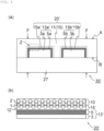
- a structure 20 including a thermistor layer 11 and two electrodes 13a and 13b (collectively referred to as reference numeral "13") is disposed on a base layer 27.
- the base layer 27 may contain a resin component.
- the resin component is not particularly limited, and may contain at least one selected from the group consisting of polyethylene terephthalate, polyetherimide, polyamideimide, polyimide, polytetrafluoroethylene, an epoxy resin, and a liquid crystal polymer (LCP).
- polyimide and polyamideimide are preferable from the viewpoint of heat resistance and adhesion.
- the base layer 27 can be, for example, a resin substrate (resin film) containing such a resin component.
- the base layer 27 is an insulating substrate.
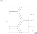
- the thermistor layer 11 is a composite (hereinafter, also referred to as a "metal oxide-containing composite") 10 including a plurality of particles (hereinafter, also simply referred to as “metal oxide particles”) 1 including a metal oxide containing at least one first metal element, and an amorphous phase (hereinafter, also referred to as a "first amorphous phase”) 2 existing between the plurality of particles 1 and containing the same metal element as the first metal element.
- a composite hereinafter, also referred to as a "metal oxide-containing composite” 10 including a plurality of particles (hereinafter, also simply referred to as “metal oxide particles”) 1 including a metal oxide containing at least one first metal element, and an amorphous phase (hereinafter, also referred to as a "first amorphous phase”) 2 existing between the plurality of particles 1 and containing the same metal element as the first metal element.
- the metal oxide constituting the metal oxide particles 1 contains at least one of Mn and Ni as the first metal element, and may further contain at least one selected from the group consisting of Fe, Al, Co, and Cu. Mn and/or Ni are essential metal elements in metal oxides. At least one selected from the group consisting of Fe, Al, Co, and Cu is an optionally added metal element in the metal oxide. The optionally added metal element is preferably at least one selected from the group consisting of Fe, Al, and Co. Any of these metal oxides may be a metal oxide semiconductor, and may particularly have a spinel-type structure, but the present invention is not limited thereto.
- the proportion of the metal element in the entire metal oxide constituting the plurality of metal oxide particles 1 is not particularly limited, and can be appropriately selected according to desired electrical characteristics and the like.
- a ratio (atomic ratio) of Mn : Ni may be, for example, 1 to 100 : 1.
- the optionally added metal element (the total of the optionally added metal elements when a plurality of the optionally added metal elements exist) may be less than the essential metal element (the total of Mn and Ni when both Mn and Ni exist), and a ratio (atomic ratio) of the essential metal element : the optionally added metal element may be, for example, 1 to 100 : 1.
- An average particle size of the metal oxide particles 1 can be, for example, 0.01 um or more and 100 um or less, and particularly 0.02 um or more and 1 um or less.
- the metal oxide particles are easily carried into gaps between other metal oxide particles by a liquid medium and/or a fluid (preferably a solvent) derived from metal acetylacetonate in the production method described later in the present embodiment, and densification of the composite obtained can be more effectively achieved.
- the average particle size is a particle size (D 50) at a point at which a cumulative value is 50% in a cumulative curve drawn by obtaining a particle size distribution on a volume basis and taking the whole to be 100%.
- the average particle size can be measured using a laser diffraction/scattering type particle size/particle size distribution measuring apparatus or an electron scanning microscope.
- the metal oxide particles 1 may be a mixture of two or more kinds of metal oxide particles having different metal oxide compositions and/or average particle sizes.
- the first amorphous phase 2 exists between the metal oxide particles 1, and can cause the metal oxide particles 1 to adhere to each other. Therefore, the composite 10 itself has high strength.
- the present embodiment is not limited, it is possible to form a structure in which the plurality of metal oxide particles 1 are dispersed in a continuous phase of the first amorphous phase 2.
- the composite 10 can contain the metal oxide particles 1 at a high density by the first amorphous phase 2 (a conductive path can be formed by the metal oxide particles 1 dispersed at a high density).
- the first amorphous phase 2 can exhibit electrical characteristics close to those of the metal oxide (semiconductor) particles 1 having a crystal structure. This makes it possible to obtain electrical characteristics similar to those of a sintered body obtained by sintering metal oxide particles at a high temperature by a conventional general method.
- the first amorphous phase 2 contains the same metal element as the first metal element contained in the metal oxide particles 1. As a result, when mutual diffusion occurs between the metal oxide particles 1 and the first amorphous phase 2, it is possible to effectively prevent the electrical characteristics of the composite 10 from deteriorating.
- the amorphous phase means a phase having substantially no crystallinity or a phase having a relatively low crystallinity, which can be distinguished and discriminated from particles having a crystal structure based on an electron beam diffraction image which is a technique known to those skilled in the art.
- the existence of the first amorphous phase 2 between the metal oxide particles 1 can mean that the first amorphous phase 2 fills a space between the plurality of metal oxide particles 1.
- a pore that may be contained in the composite 10 can be eliminated by filling with the first amorphous phase 2, so that a change in resistance value before and after being left under a high-temperature and high-humidity environment, which is considered to be caused by the pore, can be reduced.
- the first amorphous phase 2 may exist between the two metal oxide particles 1, or the two metal oxide particles 1 may be in contact with each other (the metal oxide particles are preferably bonded to each other) without substantially having the first amorphous phase 2 therebetween.
- the first amorphous phase 2 may exist with a thickness of 100 um or less.
- the thickness of the first amorphous phase 2 is preferably small from the viewpoint of electrical characteristics and/or strength. In the latter case described above, a portion where the first amorphous phase 2 is substantially absent may exist in the composite 10.
- the composite 10 (in particular, the first amorphous phase 2) is substantially free of silicon oxide such as SiO 2 glass. Silicon oxide is not preferable because it causes significant deterioration in electrical characteristics.
- the content of the silicon oxide in the composite 10 (with respect to the total mass of the metal oxide particles) is, for example, 0.1% by mass or less, preferably 0.01% by mass or less, and more preferably substantially 0% by mass.
- the composite 10 is obtained by heating (also referred to as firing, and may also be referred to as "sintering" when attention is paid to metal oxide particles) a raw material mixture (a mixture containing the metal oxide particles 1 and metal acetylacetonate) as a precursor of the composite at a temperature of 600°C or lower under pressure.
- a raw material mixture a mixture containing the metal oxide particles 1 and metal acetylacetonate
- the composite 10 can be produced by low-temperature firing.
- the two electrodes 13a and 13b are formed from at least one second metal element selected from the group consisting of Cu, Al, Ag, and Ni.
- the electrode 13 may be an alloy.
- the second metal element is preferably any one of or two or more of Ni, Cu, and Ag.
- the second metal element is inexpensive and easily available as compared with Ag-Pd (obtained by mixing and sintering Ag particles and Pd particles) as described in Patent Document 1. According to the present embodiment, it is possible not to use metal species that are expensive and poor in resources.
- the term "cosintering" means that a precursor (raw material mixture) of the thermistor layer is simultaneously subjected to heat treatment (firing) for sintering, and in the present embodiment, the base layer and the electrode are co-sintered with the thermistor layer.
- bonding layers 15a and 15b exist between the two electrodes 13a and 13b and the thermistor layer 11 (composite 10).
- the bonding layer 15 is formed by diffusing the second metal element and the resin component into the composite 10.
- a boundary between the composite 10 and the bonding layer 15 is not necessarily clear (in the accompanying drawings, a virtual boundary is indicated by a dotted line).
- the composite 10 and the bonding layer 15 may be collectively understood as a metal oxide-containing composite layer or thermistor layer.
- the composite 10 between the electrodes 13a and 13b, together with the bonding layers 15a and 15b, can act as a thermistor layer whose resistance can vary depending on temperature (more specifically with a negative temperature coefficient).
- the bonding layer 15 is formed by diffusing the second metal element derived from the electrode 13 and the resin component derived from the substrate 27 into the composite 10 (including the metal oxide particles 1 and the first amorphous phase 2).
- the second metal element can be diffused from the electrode 13 to the composite 10 by heat and dissolution (more specifically, dissolution of the metal element in metal acetylacetonate, which can occur during the application and heat treatment of a raw material mixture (mixture including metal oxide particles and metal acetylacetonate)) to form the bonding layer 15.
- the resin component can be diffused from the substrate 27 to the composite 10 by heat and dissolution (more specifically, dissolution of the resin component in metal acetylacetonate, which can occur during the application and heat treatment of a raw material mixture) to form the bonding layer 15.
- the second metal element and the resin component may diffuse into either the metal oxide particles 1 or the first amorphous phase 2, and may diffuse more into the first amorphous phase 2 in most cases. Since the first amorphous phase 2 contains the same metal element as the first metal element as described above, it can also be understood that in the bonding layer 15, the second amorphous phase 12 contains the same metal element as the first metal element, the same metal element as the second metal element, and the same element as the resin component (carbon element when the resin component contains carbon).
- the bonding layer 15 can be understood as a region in which the same metal element as the second metal element is distributed and the same element as the resin component (typically, carbon element) is distributed. Elements (particularly metal elements and carbon elements) contained in the thermistor layer and the bonding layer can be confirmed using a scanning transmission electron microscope (STEM) and/or energy dispersive X-ray spectrometry (EDX).
- STEM scanning transmission electron microscope
- EDX energy dispersive X-ray spectrometry
- the base layer 27 and the electrodes 13a and 13b can be co-sintered with the thermistor layer 11 by heating the raw material mixture for obtaining the composite 10 together with the base layer 27 and the electrodes 13a and 13b, so that the bonding layers 15a and 15b in which the second metal element and the resin component are diffused into the composite are formed between the electrodes 13a and 13b and the thermistor layer 11. Due to the bonding layers 15a and 15b thus configured, high bonding strength can be obtained between the thermistor layer 11 (composite 10) and the electrodes 13a and 13b.
- the bonding layer 15 (more specifically, the second amorphous phase 12) contains the same metal element as the first metal element and the second metal element.
- the bonding layer 15 can exhibit electrical characteristics close to those of the metal oxide (semiconductor) particles 1 having a crystal structure.
- the bonding layer 15 contains the same metal element as the first metal element and the second metal element, electrical resistance (schematically, a Schottky barrier between the metal oxide (semiconductor) particles 1 and the electrode 13, more specifically, interface resistance between the metal oxide particles 1 and the second amorphous phase 12 and between the second amorphous phase 12 and the electrode 13) between the composite 10, the bonding layer 15, and the electrode 13 can be reduced, and the electrical characteristics of the thermistor 30 can be improved.
- electrical resistance (schematically, a Schottky barrier between the metal oxide (semiconductor) particles 1 and the electrode 13, more specifically, interface resistance between the metal oxide particles 1 and the second amorphous phase 12 and between the second amorphous phase 12 and the electrode 13) between the composite 10, the bonding layer 15, and the electrode 13 can be reduced, and the electrical characteristics of the thermistor 30 can be improved.
- the composite 10 can contain the metal oxide particles 1 at a high density by the first amorphous phase 2, and the first amorphous phase 2 and the second amorphous phase 12 can exhibit electrical characteristics close to those of the metal oxide (semiconductor) particles 1; therefore, electrical characteristics similar to those of a sintered body obtained by sintering the metal oxide particles at a high temperature by a conventional general method can be obtained, and desired electrical characteristics (for example, thermistor characteristics, more specifically, room temperature resistivity, B constant, and the like) can be achieved.
- desired electrical characteristics for example, thermistor characteristics, more specifically, room temperature resistivity, B constant, and the like
- the composite 10 is firmly bonded to the electrodes 13a and 13b via the bonding layers 15a and 15b, and high bonding strength can be achieved.
- the resistance value of the thermistor 30 varies little, and high reliability can be achieved.
- initial characteristics of the thermistor 30 can be stabilized, and, in addition, the reliability of the thermistor 30 against environmental changes can be secured.
- thermistor in a conventionally known thermistor (see, for example, Patent Document 1), a metal element can be diffused from an electrode by simple heat treatment; however, in this case, oxidation of the electrode occurs, so that thermistor characteristics may be deteriorated, and it is difficult to obtain high bonding strength due to a difference in thermal expansion coefficient between the electrode and the thermistor layer.
- the thermistor 30 of the present embodiment does not impair the thermistor characteristics and can obtain high bonding strength.
- the thickness of the structure 20 (including the thermistor layer 11 and the electrodes 13a and 13b) disposed on the base layer 27 may be, for example, 100 um or less, and more specifically, may be 1 um or more and 30 um or less.
- the thermistor 30 is also referred to as a thin film thermistor.
- the thickness of the base layer 27 is not particularly limited, and may be, for example, 1 to 50 um in the case of the thin film thermistor.
- the thermistor 30 Since the thermistor 30 is thin as described above, the thermistor 30 can be easily installed in a small space. Further, it is possible to reduce physical damage due to pressurization at the time of attachment to both the thermistor 30 and an object to which the thermistor 30 is attached and at the time of operation. Furthermore, since the thermistor 30 has a small heat capacity, the thermistor 30 exhibits high temperature responsiveness. Since the composite 10 (and the bonding layers 15a and 15b) is thin and has flexibility, the composite 10 is hardly broken against deformation. In particular, when a flexible substrate (for example, a resin film) is used as the base layer 27, the thermistor 30 that is flexible as a whole can be obtained.
- a flexible substrate for example, a resin film
- the structure 20 has two surfaces A and B (these surfaces may also face a main surface of the base layer 27) facing each other, and these two surfaces A and B have irregularities smaller than the thickness of the two electrodes 13a and 13b, or are preferably flat ( FIG. 1(a) shows the case where these surfaces A and B are flat).
- the structure 20 including the thermistor layer 11 that is a metal oxide-containing composite and the electrode 13 that is a metal is greatly different in material properties such as altitude and stress deformation, and has relatively high hardness.
- the surfaces A and B of the structure 20 have small irregularities or are more preferably flat, when sandwiching is performed between two objects having flat facing surfaces and a pressure F is applied in a thickness direction of the thermistor 30, the pressure is uniformly applied to the structure 20 and the base layer 27, and the thermistor characteristics are not impaired.
- the thermistor 30 is used as a temperature sensor, an object to be measured for temperature (which may be any of the two objects) is hardly broken, and high pressure resistance is obtained.
- the surfaces A and B of the structure 20 is brought into contact with the object to be measured for temperature, the surfaces A and B have small irregularities or are more preferably flat, so that a large contact area is obtained, and thermal responsiveness is excellent. Both high pressure resistance and thermal responsiveness can be achieved only by the structure 20 (when irregularities larger than the thickness of the electrode are provided, high pressure resistance and thermal responsiveness can be achieved without forming a resin layer in order to reduce the irregularities).
- the thickness of the electrodes 13a and 13b is preferably more than 1 um in order to effectively avoid disconnection of the electrodes.
- the thickness of the electrode is minimum, the above-described effect may be minimized.
- the thermistor layer is about 1 to 10 um, the size of irregularities that can exist on the two surfaces A and B is 1 um or less, so that a sufficient effect can be obtained in terms of pressure resistance and thermal responsiveness.
- a conventionally known thermistor (see, for example, Patent Documents 1, 3, and 4) has relatively large irregularities on a surface of a structure including an electrode and a thermistor layer.
- a load is concentrated on the electrode and/or the thermistor layer having high hardness and small elastic deformation, and thermistor characteristics may be impaired.
- the thermistor is used as a temperature sensor, there is a risk that the object to be measured for temperature may be broken.
- the thermistor 30 of the present embodiment can obtain high pressure resistance and thermal responsiveness.
- the arrangement of the thermistor layer 11 and the two electrodes 13a and 13b is not particularly limited; however, as shown in FIG. 1(a) , the two electrodes 13a and 13b may be arranged on the base layer 27 to be spaced apart from each other, and the thermistor layer 11 may be disposed on the two electrodes 13a and 13b and the base layer 27.
- the number of electrodes is not limited to two, and three or more electrodes may exist in some cases.
- the electrodes 13a and 13b may be comb-shaped counter electrodes formed on the base layer 27 as shown in FIG. 3 .
- the electrodes 13a and 13b located below the thermistor layer 11 are shown in a perspective view, and the bonding layers 15a and 15b are omitted.
- the electrical characteristics of the thermistor 30 can be controlled (for example, variation in resistance value can be further reduced), and high temperature resolution can be achieved.
- the two electrodes 13a and 13b may be electrically connected to the two external electrodes 14a and 14b, respectively.
- a gap is formed in a planar direction (direction parallel to the main surface of the base layer 27) between the counter electrodes.
- the external electrodes 14a and 14b are provided on both outer sides (both outer sides in a tooth length direction L 1 ) of the pair of comb-shaped counter electrodes 13a and 13b
- extraction electrodes extending along a tooth width direction L 2 may be formed on both outer sides of the pair of comb-shaped counter electrodes 13a and 13b.
- the thermistor 30 of the present embodiment described above can be manufactured by any suitable method, and can be manufactured, for example, by the following method.
- the electrodes 13a and 13b formed from the second metal element are formed on the base layer 27.
- the electrodes 13a and 13b can be pattern-formed by any suitable method such as photolithography, plating, vapor deposition, or sputtering.
- a paste containing particles of the second metal element may be used to form precursors of the electrodes 13a and 13b, and then fired simultaneously with a precursor of the thermistor layer 11.
- a mixture (hereinafter, also referred to as "raw material mixture” in the present specification) containing the metal oxide particles 1 and the metal acetylacetonate is applied to a predetermined region (region where the composite 10 and the bonding layers 15a and 15b, in other words, the metal oxide-containing composite layer is to be formed) of the base layer 27 on which the electrodes 13a and 13b (or precursors thereof) are formed as described above, and the mixture is heated under pressure at a temperature of a melting point of the metal acetylacetonate or higher and 600°C or lower, whereby the composite 10 and the bonding layers 15a and 15b (and the electrodes 13a and 13b in the case of co-firing) are simultaneously and integrally formed in the form of a sintered body containing the metal oxide particles 1.
- the raw material mixture can be applied (for example, coating, printing (screen printing, etc.)) to a predetermined region by a method known to those skilled in the art, for example, by coating, dipping, lamination, spraying, or the like.
- the base layer to which the raw material mixture is applied can be subjected to a treatment such as drying under heating or natural drying as necessary, and then heating can be performed under pressure at a temperature of the melting point of the metal acetylacetonate or higher and 600°C or lower using means known to those skilled in the art such as a pressing machine.
- the metal acetylacetonate is an acetylacetonate salt of a metal, and more specifically, is a chelate complex having an acetylacetonate ion ((CH 3 COCHCOCH 3 ) - , hereinafter also abbreviated as (acac) -) of a bidentate ligand and a central metal.
- the metal element contained in the metal acetylacetonate is any one or two or more elements selected from the first metal element, and is preferably the same metal element as the first metal element contained in the metal oxide particles 1, but the present invention is not limited thereto.
- metal acetylacetonate one kind of metal acetylacetonate may be used, or two or more kinds of metal acetylacetonates may be used in combination.
- metal acetylacetonate one kind of metal acetylacetonate may be used, or two or more kinds of metal acetylacetonates may be used in combination.
- two or more kinds of metal acetylacetonates may be used in combination according to an existence ratio of these metal elements, but the present invention is not limited thereto.
- a raw material mixture is obtained by mixing the metal oxide particles and the metal acetylacetonate.
- the metal oxide particles and the metal acetylacetonate can be mixed in an atmosphere at normal temperature and normal humidity under atmospheric pressure.
- the metal acetylacetonate may be mixed at a ratio of, for example, 0.1% by mass or more and 50% by mass or less, and is mixed at a ratio of preferably 1% by mass or more and 30% by mass or less, and more preferably 2% by mass or more and 10% by mass or less, with respect to the total mass of the metal oxide particles.
- the metal acetylacetonate to be mixed a metal acetylacetonate in an arbitrary state may be used.
- the raw material mixture may be obtained by mixing metal oxide particles and a dried powdery solid metal acetylacetonate.
- a raw material mixture is obtained by mixing the metal oxide particles and the powdery metal acetylacetonate using a general mixing method performed, for example, in one or two or more kinds of solvents selected from the group consisting of water, acetylacetone, methanol and/or alcohol containing ethanol and the like, or in one or two or more kinds of gases selected from the group consisting of air, nitrogen and the like under atmospheric pressure.
- the raw material mixture may be obtained by mixing metal oxide particles, metal acetylacetonate, and a solvent.
- a solvent any suitable solvent can be used, and for example, one or a mixture of two or more selected from the group consisting of water, acetylacetone, an alcohol containing methanol and/or ethanol, and the like may be used.
- the amount of the solvent only needs to be not too large to an extent suitable for subjecting the raw material mixture to heating under pressure, and is not particularly limited, and the solvent can be mixed at a ratio of, for example, 50% by mass or less, preferably 30% by mass or less with respect to the total mass of the metal oxide particles.
- the metal acetylacetonate and the solvent may be used separately, or a liquid product in which the metal acetylacetonate is dispersed or dissolved in the solvent may be used. In the latter case, a liquid product obtained by synthesizing the metal acetylacetonate may be used without separating the metal acetylacetonate therefrom. More specifically, the metal acetylacetonate can be synthesized by mixing liquid acetylacetone with a metal compound (for example, metal hydroxides and chlorides), and the liquid product after synthesis can be used as it is, or by adding a solvent as necessary.
- a metal compound for example, metal hydroxides and chlorides
- the raw material mixture may further contain any suitable material to the extent that the desired electrical characteristics are not adversely affected. More specifically, the raw material mixture may further contain additives such as a pH adjusting agent, a sintering aid, and a pressure relieving agent. These additives may be mixed at a ratio of, for example, 0.01% by mass or more and 10% by mass or less, and is mixed at a ratio of preferably 0.01% by mass or more and 1% by mass or less, and more preferably 0.01% by mass or more and 0.1% by mass or less, with respect to the total mass of the metal oxide particles.
- additives such as a pH adjusting agent, a sintering aid, and a pressure relieving agent.
- the raw material mixture obtained as described above is heated under pressure at a temperature of the melting point of the metal acetylacetonate or higher and 600°C or lower, whereby a relatively high-density sintered body can be formed.
- the metal acetylacetonate is liquefied and can act as a liquid medium.
- the heating is preferably performed in the presence of a fluid.
- the fluid is, for example, a liquid, preferably a liquid that can be used as a solvent, and more preferably water.
- water exists when the raw material mixture is heated and pressurized, water exists at an interface of the metal oxide particles contained in the raw material mixture.
- the raw material mixture can be sintered at a lower temperature, and the strength of the sintered body can be effectively improved.
- the state in which the mixture is in the presence of water means that water may not be actively added to the mixture and a slight amount of water may exist at the interface of the metal oxide particles.
- the metal oxide particles may absorb moisture at room temperature.
- the active addition of water may be performed by adding (mixing) water to the raw material mixture, or may be performed by heating and pressurizing the raw material mixture under a water vapor atmosphere.
- the water can be more effectively delivered through the interface of each particle.
- the amount thereof is not particularly limited, and may be, for example, 20% by mass or less, is preferably 15% by mass or less, and is typically 10% by mass with respect to the total mass of the metal oxide particles.
- the amount of water mixed in the raw material mixture is 20% by mass or less, water can be mixed with the raw material mixture, and deterioration of moldability of the raw material mixture can be more effectively prevented.
- it is preferable to use as much water as possible within the above range specifically, water of 10% by mass or more and 20% by mass or less.
- water of more than 0% by mass and 10% by mass or less it is preferable to use as little water as possible within the above range, specifically, water of more than 0% by mass and 10% by mass or less.
- the pressurization pressure of the raw material mixture may be, for example, 1 MPa or more and 5000 MPa or less, and is preferably 5 MPa or more and 1000 MPa or less, more preferably 10 MPa or more and 500 MPa or less.
- the pressurization of the raw material mixture means that a pressing force (or a physical/mechanical pressure) is applied to the raw material mixture (more specifically, a solid component contained in the raw material mixture) by using, for example, a pressure molding machine.
- a pressing force or a physical/mechanical pressure
- the temperature at which the raw material mixture is heated refers to a firing temperature, and may be the temperature of the melting point of the metal acetylacetonate contained in the raw material mixture or higher and 600°C or lower.
- the melting point refers to a temperature measured by a measurement method defined in JIS standard at room temperature and atmospheric pressure. Each melting point changes depending on various conditions such as a pressure at the time of pressurization.
- Table 1 The melting points of various metal acetylacetonates are shown in Table 1 below.
- the "melting point of the metal acetylacetonate” refers to the highest melting point among the melting points of all the metal acetylacetonates.
- the heating temperature of the raw material mixture may be a temperature of higher by 5°C or more than the melting point of the metal acetylacetonate and 600°C or lower, for example, 100°C or higher and 600°C or lower, preferably 100°C or higher and 400°C or lower, and more preferably 100°C or higher and 300°C or lower, depending on the type of the metal oxide to be used and the like.
- the relatively high density means that the ratio of the density to the theoretical density of the sintered body obtained thereby is higher than the ratio of the density to the theoretical density of the sintered body obtained when the metal oxide particles contained in the raw material mixture are heated and pressurized alone (without the presence of the metal acetylacetonate) at the same temperature under the same pressure conditions.
- the sintered body obtained according to the present embodiment may have a relatively high density, and the ratio of the density to the theoretical density may be, for example, 70% or more, preferably 80% or more, depending on the composition of the metal oxide particles to be used and the like.
- the metal oxide contained in the obtained sintered body may be considered to be substantially the same as the metal oxide of the metal oxide particles contained in the raw material mixture.
- a time for heating and pressurizing the raw material mixture can be appropriately selected, the time is preferably 1 second or more and 120 minutes or less.
- the sintered body formed in contact with the electrode 13 (13a, 13b) using the raw material mixture containing the metal oxide particles and the metal acetylacetonate corresponds to the composite 10 containing the metal oxide particles 1 and the first amorphous phase 2 and the bonding layer 15 (15a, 15b) containing the second amorphous phase 12 as schematically shown in FIGS. 1(b) and 2 .
- the first amorphous phase 2 contains a metal element (the same metal element as the first metal element) derived from the metal acetylacetonate.
- the bonding layer 15 (second amorphous phase 12) contains the second metal element derived from the electrode 13 and the resin component derived from the base layer 27 in addition to the metal element (the same metal element as the first metal element) derived from the metal acetylacetonate.
- the heat treatment is desirably performed under a condition that the resin component of the base layer 27 is slightly melted.
- the heat treatment by heating at 270°C for 30 minutes under a pressure of 100 MPa using a heating press machine, and then annealing at 250°C for 10 hours in order to remove unnecessary organic substances that may remain.
- the thermistor 30 of the present embodiment can be manufactured.
- the present embodiment relates to a thermistor in which two electrodes include a base material formed from a second metal element and a coating layer formed on a surface of the base material and formed from a third metal element.
- a structure 20' including a thermistor layer 11 and two electrodes 13a' and 13b' (collectively referred to as reference numeral "13′′′) is disposed on a base layer 27.
- the two electrodes 13a' and 13b' include base materials 3a and 3b (collectively referred to as reference numeral “3") including at least one second metal element selected from the group consisting of Cu, Al, Ag, and Ni, and coating layers 5a and 5b (collectively referred to as reference numeral "5") formed on the surface of the base material and including at least one third metal element selected from the group consisting of Ni, Au, Ag, Pt, Pd, Zn, Cr, W, Mo, Cu, and Ti.
- the base material 3 may be an alloy.
- the second metal element is preferably any one of or two or more of Ni, Cu, and Ag.
- the coating layer 5 may be an alloy or a laminate.
- the third metal element is a metal element different from the second metal element, and it is preferable that the resistance value (to the same extent as metal elements of the base material 3, for example, Cu and Ag) is low, the surface state is hardly changed, the diffusion amount is smaller than that of the metal element of the base material 3, and the diffusion of the metal element of the base material 3 can be prevented to some extent.
- the third metal element is preferably any one or two or more of Ni, Au, Ag, Pt, Pd, Zn, Cr, W, Mo, Cu, and Ti, and more preferably Au.
- the second metal element and the third metal element are inexpensive and easily available as compared with Ag-Pd (obtained by mixing and sintering Ag particles and Pd particles) as described in Patent Document 1. According to the present embodiment, it is possible not to use metal species that are expensive and poor in resources.
- the thickness of the coating layer 5 may be appropriately selected, and may be, for example, 0.1 to 1.0 ⁇ m.
- the thermistor 30' of the present embodiment high bonding strength can be obtained between the thermistor layer 11 (composite 10) and the electrodes 13a' and 13b'.
- initial electrical characteristics resistance value and B constant
- deterioration of electrical characteristics increase in resistance value and change in B constant
- bonding layers 15a' and 15b' may exist between the two electrodes 13a' and 13b' and the thermistor layer 11 (composite 10).
- the bonding layer 15' may be formed by diffusing the third metal element and the resin component and optionally the second metal element into the composite 10.
- a boundary between the composite 10 and the bonding layer 15' is not necessarily clear (in the accompanying drawings, a virtual boundary is indicated by a dotted line).
- the composite 10 and the bonding layer 15 may be collectively understood as a metal oxide-containing composite layer or thermistor layer.
- the composite 10 between the electrodes 13a' and 13b', together with the bonding layers 15a' and 15b' can act as a thermistor layer whose resistance can vary depending on temperature (more specifically with a negative temperature coefficient).
- the bonding layer 15' is formed by diffusing the third metal element derived from the coating layer 5 and the resin component derived from the substrate 27 (and optionally the second metal element derived from the base material 3) into the composite 10 (including the metal oxide particles 1 and the first amorphous phase 2).
- the third metal element (and the second metal element if exists) can be diffused from the electrode 13' to the composite 10 by heat and dissolution (more specifically, dissolution of the metal element in metal acetylacetonate, which can occur during the application and heat treatment of a raw material mixture (mixture including metal oxide particles and metal acetylacetonate)) to form the bonding layer 15'.
- the resin component can be diffused from the substrate 27 to the composite 10 by heat and dissolution (more specifically, dissolution of the resin component in metal acetylacetonate, which can occur during the application and heat treatment of a raw material mixture) to form the bonding layer 15'.
- the third metal element (and the second metal element when exists) and the resin component may diffuse into either the metal oxide particles 1 or the first amorphous phase 2, and may diffuse more into the first amorphous phase 2 in most cases.
- the first amorphous phase 2 contains the same metal element as the first metal element as described above, it can also be understood that in the bonding layer 15', the second amorphous phase 12' contains the same metal element as the first metal element, the same metal element as the third metal element (and the same metal element as the second metal element when present), and the same element as the resin component (carbon element when the resin component contains carbon).
- the bonding layer 15' can be understood as a region in which the same metal element as the third metal element is distributed and the same element as the resin component (typically, carbon element) is distributed.
- the bonding layer 15' (more specifically, the second amorphous phase 12') contains the same metal elements as the first metal element and the third metal element (and the second metal element when exists).
- the bonding layer 15' can exhibit electrical characteristics close to those of the metal oxide (semiconductor) particles 1 having a crystal structure.
- the bonding layer 15' contains the same metal elements as the first metal element and the third metal element (and the second metal element when exists), electrical resistance (schematically, a Schottky barrier between the metal oxide (semiconductor) particles 1 and the electrode 13', more specifically, interface resistance between the metal oxide particles 1 and the second amorphous phase 12' and between the second amorphous phase 12' and the electrode 13) between the composite 10, the bonding layer 15', and the electrode 13' can be reduced, and the electrical characteristics of the thermistor 30' can be improved.
- Embodiment 1 The same description as that of Embodiment 1 can be applied to the present embodiment.
- the thermistor 30' of the present embodiment described above can be manufactured by any suitable method, and can be manufactured, for example, by the following method.
- the base materials 3a and 3b formed from the second metal element are formed on the base layer 27.
- the base materials 3a and 3b can be pattern-formed by any suitable method such as photolithography, plating, vapor deposition, or sputtering.
- the coating layers 5a and 5b formed from the third metal element are formed on the surfaces of the base materials 3 and 3b.
- the coating layers 5a and 5b can be formed by any suitable method such as plating.
- the electrodes 13a' and 13b' are formed.
- the bonding layer 15' (second amorphous phase 12') contains the third metal element derived from the electrode 13' (and the second metal element when exists) and the resin component derived from the base layer 27 in addition to the metal element (the same metal element as the first metal element) derived from the metal acetylacetonate.
- the thermistor 30' of the present embodiment can be manufactured.
- the bonding layers 15a' and 15b' and the thermistor layer 11 may not be distinguishable.
- the thermistor layer 11 may be formed by diffusing the third metal element and the resin component and optionally the second metal element into the composite 10.
- Example 1 relates to a thermistor provided with a pair of comb-shaped counter electrodes formed from Cu in the aspect described above in Embodiment 1.
- metal oxide particles having an average particle diameter of about 0.2 um and containing Mn : Ni : Co at a ratio of 3 : 1 : 2 (atomic ratio) manganese acetylacetonate was added at a ratio of 10% by mass (with respect to the total mass of the metal oxide particles), ethanol was added as a solvent, and the resultant mixture was mixed for 16 hours to obtain a raw material mixture in a slurry form.
- a Cu layer having a thickness of 10 um was pattern-formed by photolithography on a base layer which was a polyimide film having a thickness of 10 um, and the pair of comb-shaped counter electrodes was prepared together with an extraction electrode.
- the pair of comb-shaped counter electrodes had a total area dimension of 1.5 mm (dimension in a direction along a length direction of a tooth) ⁇ 3.0 mm (dimension in a direction along a width direction of the tooth) as viewed from above, and the extraction electrode was formed on each of both outer sides of the pair of comb-shaped counter electrodes with 0.5 mm (dimension in the direction along the length direction of the tooth) ⁇ 4.5 mm (dimension in the direction along the width direction of the tooth) (see FIG. 5(a) ).
- the raw material mixture obtained above was supplied in the form of a sheet having a thickness of 15 ⁇ m by a doctor blade method onto an exposed surface of the electrode and the base layer to obtain a precursor laminate (see FIG. 5(b) ).
- the precursor laminate was dried at 100°C for 10 hours, then heated at 270°C for 30 minutes under a pressure of 100 MPa using a heating press machine, and then annealed at 250°C for 10 hours in order to remove unnecessary organic substances that may remain, thereby obtaining a laminate (thus, it was considered that the metal oxide-containing composite was formed together with the bonding layer).
- the obtained laminate was cut with a dicing saw to obtain a thermistor sample having a dimension of 3.0 mm ⁇ 4.5 mm as viewed from the top and a total thickness of 30 um as shown in FIGS. 5(a) to 5(b) .
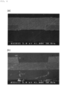
- the thermistor sample of Example 1 obtained thereby was embedded in a resin, cut into two parts through the width direction of the teeth of the comb-shaped electrode, and the section was observed with a field emission scanning electron microscope (FE-SEM) observation.
- the results are shown in FIG. 6(a) . From FIG. 6(a) , it was confirmed that the lowermost layer was a polyimide base layer, two Cu electrodes were provided on the left and right sides on the polyimide base layer, and a thermistor layer of a metal oxide-containing composite was formed on the polyimide base layer and the two Cu electrodes (the layer above the thermistor layer was a resin used for embedding the sample).
- Comparative Example 1 related to an example in which a precursor of a thermistor layer was disposed on a base layer (metal substrate) formed from Cu or Ni and co-sintered, and an example in which a split electrode was formed thereon and an attempt was made to prepare a thermistor. It should be noted that in the thermistor of Patent Document 1, a gap is formed in the vertical direction (direction perpendicular to the main surface of the substrate) between the metal substrate and the comb-shaped counter electrode.
- an organic binder was added at a ratio of 10% by mass (with respect to the total mass of the metal oxide particles), ethanol was added as a solvent, and the resultant mixture was mixed for 16 hours to obtain a raw material mixture in a slurry form.
- the raw material mixture obtained above was supplied in the form of a sheet having a thickness of 15 um by the doctor blade method onto a base layer which was a Cu foil or a Ni foil having a thickness of 20 um to obtain a precursor laminate.
- the precursor laminate was housed in a zirconia box, heated at 300°C for 100 hours in a nitrogen atmosphere to remove the organic binder, and then fired at 800 to 1300°C for 60 minutes in a reducing atmosphere in the box to obtain a sintered body.
- Comparative Example 2 related to a thermistor in which a metal oxide-containing composite capable of acting as a thermistor layer was prepared, a base layer containing a resin component was then formed, and a pair of comb-shaped counter electrodes formed from Cu was then provided.
- the precursor laminate was dried at 100°C for 10 hours, then heated at 270°C for 30 minutes under a pressure of 100 MPa using a heating press machine, and then annealed at 250°C for 10 hours in order to remove unnecessary organic substances that may remain, thereby obtaining a laminate (thus, it was considered that the metal oxide-containing composite was formed). Thereafter, a precursor liquid of polyamideimide was applied in a thickness of 15 um onto a film (metal oxide-containing composite capable of functioning as the thermistor layer) derived from the sheet in the obtained laminate, and heated at 250°C for 1 hour to thermally cure the polyamideimide, and thus to form a resin substrate.
- a precursor liquid of polyamideimide was applied in a thickness of 15 um onto a film (metal oxide-containing composite capable of functioning as the thermistor layer) derived from the sheet in the obtained laminate, and heated at 250°C for 1 hour to thermally cure the polyamideimide, and thus to form a resin substrate.
- a Cu foil on a side opposite to the resin substrate was pattern-formed by photolithography (more specifically, a photoresist was applied to the surface of the copper foil, exposed in a predetermined pattern, and developed, a predetermined portion of the Cu foil was etched and removed, and the remaining resist was removed), and the pair of comb-shaped counter electrodes was provided together with an extraction electrode in the same manner as in Example 1.
- the obtained laminate was cut with a dicing saw to obtain a thermistor sample having a dimension of 3.0 mm ⁇ 4.5 mm as viewed from the top and a total thickness of 30 um in the same manner as in Example 1.
- the section was observed with a field emission scanning electron microscope (FE-SEM) observation in the same manner as in Example 1.
- FE-SEM field emission scanning electron microscope
- FIG. 6(b) From FIG. 6(b) , it was confirmed that the lowermost layer was a polyamideimide base layer, a thermistor layer of a metal oxide-containing composite was formed on the base layer was formed, and the two Cu electrodes were formed on the left and right sides on the thermistor layer (the layer above the two Cu electrodes and the thermistor layer was a resin used for embedding the sample).
- Example 2 relates to a thermistor provided with a pair of comb-shaped counter electrodes in which the base material made of Cu was covered with a coating layer formed from Ni in the aspect described above in Embodiment 2.
- metal oxide particles having an average particle diameter of about 0.2 um and containing Mn : Ni : Co at a ratio of 3 : 1 : 2 (atomic ratio) manganese acetylacetonate was added at a ratio of 10% by mass (with respect to the total mass of the metal oxide particles), ethanol was added as a solvent, and the resultant mixture was mixed for 16 hours to obtain a raw material mixture in a slurry form.
- a Cu layer having a thickness of 10 um was pattern-formed by photolithography on a base layer which was a polyimide film having a thickness of 10 um to obtain a base material, a Ni layer having a thickness of 1 to 5um was further formed by plating treatment on the surface of the base material, and a pair of comb-shaped counter electrodes were produced together with an extraction electrode in the same dimension as in Example 1.
- the raw material mixture obtained above was supplied in the form of a sheet having a thickness of 15 um by a doctor blade method onto an exposed surface of the electrode and the base layer to obtain a precursor laminate.
- the precursor laminate was dried at 100°C for 10 hours, then heated at 270°C for 30 minutes under a pressure of 100 MPa using a heating press machine, and then annealed at 250°C for 10 hours in order to remove unnecessary organic substances that may remain, thereby obtaining a laminate (thus, it was considered that the metal oxide-containing composite was preferably formed together with the bonding layer).
- the obtained laminate was cut with a dicing saw to obtain a thermistor sample having the same dimensions and total thickness as in Example 1 when viewed from above.
- Example 3 was a modification of Example 2 and related to a thermistor provided with a pair of comb-shaped counter electrodes in which a base material made of Cu was covered with a coating layer formed from Au.
- metal oxide particles having an average particle diameter of about 0.2 um and containing Mn : Ni : Co at a ratio of 3 : 1 : 2 (atomic ratio) manganese acetylacetonate was added at a ratio of 10% by mass (with respect to the total mass of the metal oxide particles), ethanol was added as a solvent, and the resultant mixture was mixed for 16 hours to obtain a raw material mixture in a slurry form.
- a Cu layer having a thickness of 10 um was pattern-formed by photolithography on a base layer which was a polyimide film having a thickness of 10 um to obtain a base material, an Au layer having a thickness of 0.1 to 0.5 um was further formed by plating treatment on the surface of the base material, and a pair of comb-shaped counter electrodes were produced together with an extraction electrode in the same dimension as in Example 1.
- the raw material mixture obtained above was supplied in the form of a sheet having a thickness of 15 um by a doctor blade method onto an exposed surface of the electrode and the base layer to obtain a precursor laminate.
- the precursor laminate was dried at 100°C for 10 hours, then heated at 270°C for 30 minutes under a pressure of 100 MPa using a heating press machine, and then annealed at 250°C for 10 hours in order to remove unnecessary organic substances that may remain, thereby obtaining a laminate (thus, it was considered that the metal oxide-containing composite was preferably formed together with the bonding layer).
- the obtained laminate was cut with a dicing saw to obtain a thermistor sample having the same dimensions and total thickness as in Example 1 when viewed from above.
- thermoistor samples prepared in Examples 1 to 3 and Comparative Example 2 were evaluated as follows.
- the resin component (detected as element C) of the base layer is diffused into the metal oxide-containing composite by heat and dissolution (dissolution in metal acetylacetonate), and Cu of the electrode is diffused into the metal oxide-containing composite by heat and dissolution (dissolution in metal acetylacetonate), whereby the bonding layer formed between the electrode and the thermistor layer becomes one in which the resin component derived from the base layer and Cu derived from the electrode are diffused into the metal oxide-containing composite.
- the element C detected in the thermistors sample of Examples 1 to 3 may be considered to be derived from the resin component.
- the temperature is equal to or higher than a decomposition temperature of the metal acetylacetonate
- the element C derived from the metal acetylacetonate is substantially absent or very little when exists.
- the C element is derived from the resin component of the base layer. This is because the element C derived from the metal acetylacetonate should be uniformly distributed in the thermistor layer.
- the thermistor samples of Examples 1 to 3 provide higher bonding strength (adhesiveness) than the thermistor sample of Comparative Example 2.
- the thermistor samples of Examples 1 to 3 and Comparative Example 2 were cut into two parts through the width direction of the teeth of the comb-shaped electrode, and a sectional piece was cut out by a focused ion beam (FIB) and observed with scanning transmission electron microscope (STEM, JEOL JEM-F 200) observation.
- the observation site was subjected to energy dispersive X-ray analysis (EDX, Noran system 7) to identify an element existing from intensity at each applied voltage.
- EDX energy dispersive X-ray analysis
- the C element could be identified from the peak around 0.2 eV
- the Cu element could be identified from the peak around 1.0 eV
- the diffusion of each element could be confirmed.
- the thermistor samples of Example 1 and Comparative Example 2 were subjected to a strength test (pressure resistance). More specifically, the thermistor sample was sandwiched between disk-shaped iron jigs having a diameter of 50 mm and a thickness of 25 mm, and pressurization at 0.5 tons was repeated five times to confirm a change in the measured resistance value. During the measurement of the resistance value, a load (pressure) was measured by sandwiching a pressure-sensitive film Prescale for intermediate pressure (detection sensitivity: 10 MPa) manufactured by FUJIFILM Corporation between the surface of the thermistor sample opposite to the substrate and the iron jig, and a load distribution was examined.
- a strength test pressure resistance
- a rate of change in resistance value (the resistance value at the same temperature without pressurization was used as a reference) at the time of pressurization was 3% or less. Under pressure, an error of 1°C or less as a temperature sensor could be realized.
- the load (pressure) measurement with the pressure-sensitive film confirmed that the load was applied not only to the region where the electrode existed but also to the entire surface of the thermistor sample. Considering that the region where the electrode exists occupies about 30% of the entire area of the sample, it is considered that the load applied to the electrode is reduced to about 1/3 by uniformly dispersing the load in the entire area, and as a result, the rate of change in the resistance value can be reduced.
- the rate of change in the resistance value in the resistance value measurement of the first pressurization was 5% or more, and thereafter, the rate of change in the resistance value increased with the number of times.
- the load (pressure) measurement with the pressure-sensitive film confirmed that the load was concentrated only in the region where the electrode of the thermistor sample existed, and in particular, the load was biased in a region corresponding to a corner portion of the electrode.
- the thermistor sample after the measurement was observed it was confirmed that the electrode was buried in the thermistor layer and the thermistor layer was cracked.
- thermistor samples were prepared for each of Examples 1 to 3, and the initial electrical characteristics (resistance value and B constant) were evaluated. More specifically, regarding the resistance value, an average value of resistance values ( ⁇ ) measured twice at 25°C for one thermistor sample was defined as a resistance value of the thermistor sample, and the average value, standard deviation, maximum value, and minimum value of the resistance values ( ⁇ ) of the ten thermistor samples for each Example were calculated. The results are shown in Table 2. For the B constant, the B constant (-) of one thermistor sample was calculated using the resistance values ( ⁇ ) measured at 25°C and 35°C, and the average value, standard deviation, maximum value, and minimum value of the B constants of ten thermistor samples were calculated for each Example.
- Example 3 As shown in Table 2, the resistance value (average value) was smaller and the variation (standard deviation) was also smaller in Example 3 than in Examples 1 and 2.
- the B constant (average value) close to the B constant of the powder referred to as the B constant in a metal oxide sintered body (simple substance) obtained by sintering metal oxide particles having the same metal ratio as in Example at a temperature of 1000°C or higher, and was specifically 3700; the same applied to the following) was obtained, and the variation (standard deviation) was also small.
- Example 1 it is presumed that Cu of the Cu electrode is diffused into the metal oxide-containing composite at the time of heating and pressurization, and the initial resistance value is not as low as that in Example 3 due to the formed bonding layer.
- Example 2 it is presumed that Cu and Ni of the Cu base material and Ni of the coating layer are diffused into the metal oxide-containing composite at the time of heating and pressurization, and the initial resistance value is not as low as that in Example 3 due to the formed bonding layer.
- Example 3 Au in the Au coating layer has a sufficiently low resistance value, the surface state is hardly changed at the time of heating and pressurization, and diffusion of Cu in the Cu base material into the metal oxide-containing composite can be prevented to some extent, so that a sufficiently low resistance value is obtained, and the B constant (average value) close to the B constant (3700) of the powder is obtained.
- thermistor samples were prepared for each of Examples 1 to 3, and subjected to a high-temperature and high-humidity environment test to examine a rate of change in electrical characteristics (resistance value and B constant). More specifically, all thermistor samples were allowed to stand for 24 hours in a high-temperature and high-humidity environment at a temperature of 60°C and a humidity of 95% with a small environmental tester, and then the resistance value ( ⁇ ) and the B constant (-) were calculated in the same manner as described above.
- the resistance value change rate (%) based on the initial resistance value ( ⁇ ) was calculated, and the average value, standard deviation, maximum value, and minimum value of the resistance value change rates of ten thermistor samples for each Example were calculated.
- the results are shown in Table 4.
- the B constant change rate (%) based on the initial B constant (-) was calculated, and the average value, standard deviation, maximum value, and minimum value of B constant change rates of ten thermistor samples for each Example were calculated. The results are shown in Table 5.
- the resistance value increased after the high-temperature and high-humidity environment test in all thermistor samples (the minimum value was a positive value).
- the B constant increased or decreased after the high-temperature and high-humidity environment test (the minimum value was a negative value).
- the resistance value change rate and the B constant change rate (average value) were smaller and the variations (standard deviations) thereof were also smaller in Example 3 than in Examples 1 and 2. That is, in Example 3, a thermistor having little change in electrical characteristics when exposed to the high-temperature and high-humidity environment could be obtained.
- Example 1 it is presumed that Cu of the Cu electrode is diffused into the metal oxide-containing composite at the time of heating and pressurization, and the rate of change in the resistance value and the B constant under the high-temperature and high-humidity environment is larger than that in Example 3 due to the formed bonding layer.
- Example 2 it is presumed that Cu and Ni of the Cu base material and Ni of the coating layer are diffused into the metal oxide-containing composite at the time of heating and pressurization, and the rate of change in the resistance value and the B constant under the high-temperature and high-humidity environment is larger than that in Example 3 due to the formed bonding layer.
- Example 3 Au in the Au coating layer has a sufficiently low resistance value, the surface state is hardly changed at the time of heating and pressurization, and diffusion of Cu in the Cu base material into the metal oxide-containing composite can be prevented to some extent, so that the rate of change in the resistance value and the B constant under the high-temperature and high-humidity environment can be remarkably reduced.
- the thermistor of the present invention can be used in a wide variety of applications such as a temperature sensor.
- a temperature sensor such as a thermocouple
- the thermistor of the present invention can be used as a flexible temperature sensor, for example, in applications such as temperature measurement for temperature management of in-vehicle batteries and batteries for smart phones in which firing or deterioration at high temperatures is a problem, and body temperature measurement in the medical and healthcare fields.
- the thermistor of the present invention is not limited to such an application.
Landscapes
- Engineering & Computer Science (AREA)
- Microelectronics & Electronic Packaging (AREA)
- Physics & Mathematics (AREA)
- Electromagnetism (AREA)
- Thermistors And Varistors (AREA)
Applications Claiming Priority (2)
| Application Number | Priority Date | Filing Date | Title |
|---|---|---|---|
| JP2020110348 | 2020-06-26 | ||
| PCT/JP2021/005925 WO2021261006A1 (fr) | 2020-06-26 | 2021-02-17 | Thermistance |
Publications (2)
| Publication Number | Publication Date |
|---|---|
| EP4138099A1 true EP4138099A1 (fr) | 2023-02-22 |
| EP4138099A4 EP4138099A4 (fr) | 2024-07-10 |
Family
ID=79282217
Family Applications (1)
| Application Number | Title | Priority Date | Filing Date |
|---|---|---|---|
| EP21829815.6A Pending EP4138099A4 (fr) | 2020-06-26 | 2021-02-17 | Thermistance |
Country Status (5)
| Country | Link |
|---|---|
| US (1) | US12500013B2 (fr) |
| EP (1) | EP4138099A4 (fr) |
| JP (1) | JP7567912B2 (fr) |
| CN (1) | CN115720676B (fr) |
| WO (1) | WO2021261006A1 (fr) |
Family Cites Families (20)
| Publication number | Priority date | Publication date | Assignee | Title |
|---|---|---|---|---|
| WO1986007489A1 (fr) * | 1985-06-10 | 1986-12-18 | Takeuchi Press Industries Co., Ltd. | Composition magnetique liee par de la resine et procede de production d'un moulage magnetique a partir de ladite composition |
| US5916834A (en) * | 1996-12-27 | 1999-06-29 | Kyocera Corporation | Dielectric ceramics |
| US6329058B1 (en) * | 1998-07-30 | 2001-12-11 | 3M Innovative Properties Company | Nanosize metal oxide particles for producing transparent metal oxide colloids and ceramers |
| JP2000266608A (ja) * | 1999-03-15 | 2000-09-29 | Murata Mfg Co Ltd | 温度センサ |
| DE10141910B4 (de) * | 2000-08-28 | 2008-10-16 | Kyocera Corp. | Glaskeramiksinterprodukt und Verfahren zu seiner Herstellung |
| EP2472529B1 (fr) | 2009-08-28 | 2017-09-27 | Murata Manufacturing Co., Ltd. | Thermistance et procédé de production associé |
| JP5494833B2 (ja) * | 2011-01-07 | 2014-05-21 | 株式会社村田製作所 | 温度センサおよび温度センサ取り付け構造 |
| JP5776941B2 (ja) * | 2012-03-29 | 2015-09-09 | 三菱マテリアル株式会社 | 温度センサ及びその製造方法 |
| JP5871190B2 (ja) * | 2012-03-30 | 2016-03-01 | 三菱マテリアル株式会社 | サーミスタ用金属窒化物膜及びその製造方法並びにフィルム型サーミスタセンサ |
| WO2014083898A1 (fr) * | 2012-11-28 | 2014-06-05 | 株式会社村田製作所 | Dispositif à thermistance |
| JP6579194B2 (ja) * | 2015-07-31 | 2019-09-25 | 株式会社村田製作所 | 温度センサ |
| WO2018012015A1 (fr) * | 2016-07-14 | 2018-01-18 | 三井金属鉱業株式会社 | Matière active de cathode pour batterie rechargeable au lithium tout solide |
| EP3373310A1 (fr) | 2017-03-06 | 2018-09-12 | Nederlandse Organisatie voor toegepast- natuurwetenschappelijk onderzoek TNO | Sonde de température imprimée |
| JP2018151227A (ja) * | 2017-03-13 | 2018-09-27 | 三菱マテリアル株式会社 | 温度センサ |
| JP6769373B2 (ja) | 2017-03-29 | 2020-10-14 | 三菱マテリアル株式会社 | 温度センサ及びその製造方法 |
| WO2019008711A1 (fr) * | 2017-07-05 | 2019-01-10 | 株式会社村田製作所 | Procédé de production d'un corps fritté |
| JP2019096805A (ja) | 2017-11-27 | 2019-06-20 | 三菱マテリアル株式会社 | サーミスタ及びその製造方法並びにサーミスタセンサ |
| JP7234573B2 (ja) * | 2017-12-25 | 2023-03-08 | 三菱マテリアル株式会社 | サーミスタ及びその製造方法並びにサーミスタセンサ |
| JP2019138798A (ja) | 2018-02-13 | 2019-08-22 | 三菱マテリアル株式会社 | 温度センサ |
| JP2020110348A (ja) | 2019-01-11 | 2020-07-27 | Toto株式会社 | タオルハンガー |
-
2021
- 2021-02-17 EP EP21829815.6A patent/EP4138099A4/fr active Pending
- 2021-02-17 JP JP2022532285A patent/JP7567912B2/ja active Active
- 2021-02-17 CN CN202180045520.2A patent/CN115720676B/zh active Active
- 2021-02-17 WO PCT/JP2021/005925 patent/WO2021261006A1/fr not_active Ceased
-
2022
- 2022-12-13 US US18/065,125 patent/US12500013B2/en active Active
Also Published As
| Publication number | Publication date |
|---|---|
| US12500013B2 (en) | 2025-12-16 |
| JP7567912B2 (ja) | 2024-10-16 |
| US20230112895A1 (en) | 2023-04-13 |
| CN115720676B (zh) | 2026-04-14 |
| CN115720676A (zh) | 2023-02-28 |
| JPWO2021261006A1 (fr) | 2021-12-30 |
| EP4138099A4 (fr) | 2024-07-10 |
| WO2021261006A1 (fr) | 2021-12-30 |
Similar Documents
| Publication | Publication Date | Title |
|---|---|---|
| CN103077823B (zh) | 陶瓷电子部件及其制造方法 | |
| EP2472529B1 (fr) | Thermistance et procédé de production associé | |
| JP5088029B2 (ja) | バリスタ | |
| JP2012019159A (ja) | セラミック電子部品 | |
| US20030150563A1 (en) | Joined ceramic article, substrate holding structure and apparatus for treating substrate | |
| EP2680278B1 (fr) | Structure de montage pour composants électroniques | |
| EP2549491A1 (fr) | Thermistance céramique à coefficient négatif montable en surface basé sur du Mn, Co and Ti | |
| EP2937441A1 (fr) | Matériau de thermistance en nitrure de métal, procédé de fabrication s'y rapportant, et capteur à thermistance de type film | |
| US12500013B2 (en) | Thermistor | |
| CN105706188B (zh) | 变阻器用烧结体和使用其的多层基板、以及它们的制造方法 | |
| CN113053621B (zh) | 层叠线圈部件以及设计方法 | |
| US8508325B2 (en) | Chip varistor and chip varistor manufacturing method | |
| JP5725845B2 (ja) | プローブカード用セラミック配線基板およびこれを用いたプローブカード | |
| US12482584B2 (en) | Composite, and structure and thermistor using the same | |
| EP4316694A1 (fr) | Structure de joint | |
| KR102869025B1 (ko) | 회로기판의 제조방법 | |
| US20140232514A1 (en) | Thermistor and method for manufacturing the same | |
| EP3961694B1 (fr) | Module de composant électronique et substrat de circuit de nitrure de silicium | |
| CN103107105B (zh) | 多芯片组件同质键合系统质量一致性改进方法 | |
| EP4708336A1 (fr) | Thermistance à caractéristique négative | |
| EP4234518A1 (fr) | Corps assemblé, carte de circuit imprimé cuivre-céramique et dispositif à semi-conducteur | |
| WO2026009678A1 (fr) | Dispositif de mandrin électrostatique, procédé de fabrication de dispositif de mandrin électrostatique et procédé de fabrication d'empilement | |
| WO2024236846A1 (fr) | Composant électronique et procédé de formation de film | |
| JP5304772B2 (ja) | チップバリスタ及びチップバリスタの製造方法 | |
| JP2023150954A (ja) | コイル部品 |
Legal Events
| Date | Code | Title | Description |
|---|---|---|---|
| STAA | Information on the status of an ep patent application or granted ep patent |
Free format text: STATUS: THE INTERNATIONAL PUBLICATION HAS BEEN MADE |
|
| PUAI | Public reference made under article 153(3) epc to a published international application that has entered the european phase |
Free format text: ORIGINAL CODE: 0009012 |
|
| STAA | Information on the status of an ep patent application or granted ep patent |
Free format text: STATUS: REQUEST FOR EXAMINATION WAS MADE |
|
| 17P | Request for examination filed |
Effective date: 20221118 |
|
| AK | Designated contracting states |
Kind code of ref document: A1 Designated state(s): AL AT BE BG CH CY CZ DE DK EE ES FI FR GB GR HR HU IE IS IT LI LT LU LV MC MK MT NL NO PL PT RO RS SE SI SK SM TR |
|
| DAV | Request for validation of the european patent (deleted) | ||
| DAX | Request for extension of the european patent (deleted) | ||
| A4 | Supplementary search report drawn up and despatched |
Effective date: 20240611 |
|
| RIC1 | Information provided on ipc code assigned before grant |
Ipc: H01C 7/04 20060101AFI20240605BHEP |