EP4138224B1 - Elektrischer hochspannungsverbinder mit plattiertem kontaktknopf und verfahren zu seiner herstellung - Google Patents
Elektrischer hochspannungsverbinder mit plattiertem kontaktknopf und verfahren zu seiner herstellung Download PDFInfo
- Publication number
- EP4138224B1 EP4138224B1 EP22190196.0A EP22190196A EP4138224B1 EP 4138224 B1 EP4138224 B1 EP 4138224B1 EP 22190196 A EP22190196 A EP 22190196A EP 4138224 B1 EP4138224 B1 EP 4138224B1
- Authority
- EP
- European Patent Office
- Prior art keywords
- bus bar
- electrical
- electrical connector
- contact button
- contact
- Prior art date
- Legal status (The legal status is an assumption and is not a legal conclusion. Google has not performed a legal analysis and makes no representation as to the accuracy of the status listed.)
- Active
Links
Images



Classifications
-
- H—ELECTRICITY
- H01—ELECTRIC ELEMENTS
- H01R—ELECTRICALLY-CONDUCTIVE CONNECTIONS; STRUCTURAL ASSOCIATIONS OF A PLURALITY OF MUTUALLY-INSULATED ELECTRICAL CONNECTING ELEMENTS; COUPLING DEVICES; CURRENT COLLECTORS
- H01R4/00—Electrically-conductive connections between two or more conductive members in direct contact, i.e. touching one another; Means for effecting or maintaining such contact; Electrically-conductive connections having two or more spaced connecting locations for conductors and using contact members penetrating insulation
- H01R4/28—Clamped connections, spring connections
-
- H—ELECTRICITY
- H01—ELECTRIC ELEMENTS
- H01R—ELECTRICALLY-CONDUCTIVE CONNECTIONS; STRUCTURAL ASSOCIATIONS OF A PLURALITY OF MUTUALLY-INSULATED ELECTRICAL CONNECTING ELEMENTS; COUPLING DEVICES; CURRENT COLLECTORS
- H01R13/00—Details of coupling devices of the kinds covered by groups H01R12/70 or H01R24/00 - H01R33/00
- H01R13/02—Contact members
- H01R13/03—Contact members characterised by the material, e.g. plating, or coating materials
-
- H—ELECTRICITY
- H01—ELECTRIC ELEMENTS
- H01R—ELECTRICALLY-CONDUCTIVE CONNECTIONS; STRUCTURAL ASSOCIATIONS OF A PLURALITY OF MUTUALLY-INSULATED ELECTRICAL CONNECTING ELEMENTS; COUPLING DEVICES; CURRENT COLLECTORS
- H01R13/00—Details of coupling devices of the kinds covered by groups H01R12/70 or H01R24/00 - H01R33/00
- H01R13/02—Contact members
- H01R13/15—Pins, blades or sockets having separate spring member for producing or increasing contact pressure
-
- H—ELECTRICITY
- H01—ELECTRIC ELEMENTS
- H01R—ELECTRICALLY-CONDUCTIVE CONNECTIONS; STRUCTURAL ASSOCIATIONS OF A PLURALITY OF MUTUALLY-INSULATED ELECTRICAL CONNECTING ELEMENTS; COUPLING DEVICES; CURRENT COLLECTORS
- H01R13/00—Details of coupling devices of the kinds covered by groups H01R12/70 or H01R24/00 - H01R33/00
- H01R13/02—Contact members
- H01R13/15—Pins, blades or sockets having separate spring member for producing or increasing contact pressure
- H01R13/187—Pins, blades or sockets having separate spring member for producing or increasing contact pressure with spring member in the socket
-
- H—ELECTRICITY
- H01—ELECTRIC ELEMENTS
- H01R—ELECTRICALLY-CONDUCTIVE CONNECTIONS; STRUCTURAL ASSOCIATIONS OF A PLURALITY OF MUTUALLY-INSULATED ELECTRICAL CONNECTING ELEMENTS; COUPLING DEVICES; CURRENT COLLECTORS
- H01R13/00—Details of coupling devices of the kinds covered by groups H01R12/70 or H01R24/00 - H01R33/00
- H01R13/02—Contact members
- H01R13/22—Contacts for co-operating by abutting
-
- H—ELECTRICITY
- H01—ELECTRIC ELEMENTS
- H01R—ELECTRICALLY-CONDUCTIVE CONNECTIONS; STRUCTURAL ASSOCIATIONS OF A PLURALITY OF MUTUALLY-INSULATED ELECTRICAL CONNECTING ELEMENTS; COUPLING DEVICES; CURRENT COLLECTORS
- H01R25/00—Coupling parts adapted for simultaneous co-operation with two or more identical counterparts, e.g. for distributing energy to two or more circuits
- H01R25/14—Rails or bus-bars constructed so that the counterparts can be connected thereto at any point along their length
-
- H—ELECTRICITY
- H01—ELECTRIC ELEMENTS
- H01R—ELECTRICALLY-CONDUCTIVE CONNECTIONS; STRUCTURAL ASSOCIATIONS OF A PLURALITY OF MUTUALLY-INSULATED ELECTRICAL CONNECTING ELEMENTS; COUPLING DEVICES; CURRENT COLLECTORS
- H01R4/00—Electrically-conductive connections between two or more conductive members in direct contact, i.e. touching one another; Means for effecting or maintaining such contact; Electrically-conductive connections having two or more spaced connecting locations for conductors and using contact members penetrating insulation
- H01R4/02—Soldered or welded connections
-
- H—ELECTRICITY
- H01—ELECTRIC ELEMENTS
- H01R—ELECTRICALLY-CONDUCTIVE CONNECTIONS; STRUCTURAL ASSOCIATIONS OF A PLURALITY OF MUTUALLY-INSULATED ELECTRICAL CONNECTING ELEMENTS; COUPLING DEVICES; CURRENT COLLECTORS
- H01R13/00—Details of coupling devices of the kinds covered by groups H01R12/70 or H01R24/00 - H01R33/00
- H01R13/02—Contact members
- H01R13/10—Sockets for co-operation with pins or blades
- H01R13/11—Resilient sockets
- H01R13/113—Resilient sockets co-operating with pins or blades having a rectangular transverse section
-
- H—ELECTRICITY
- H01—ELECTRIC ELEMENTS
- H01R—ELECTRICALLY-CONDUCTIVE CONNECTIONS; STRUCTURAL ASSOCIATIONS OF A PLURALITY OF MUTUALLY-INSULATED ELECTRICAL CONNECTING ELEMENTS; COUPLING DEVICES; CURRENT COLLECTORS
- H01R2201/00—Connectors or connections adapted for particular applications
- H01R2201/26—Connectors or connections adapted for particular applications for vehicles
-
- H—ELECTRICITY
- H01—ELECTRIC ELEMENTS
- H01R—ELECTRICALLY-CONDUCTIVE CONNECTIONS; STRUCTURAL ASSOCIATIONS OF A PLURALITY OF MUTUALLY-INSULATED ELECTRICAL CONNECTING ELEMENTS; COUPLING DEVICES; CURRENT COLLECTORS
- H01R43/00—Apparatus or processes specially adapted for manufacturing, assembling, maintaining, or repairing of line connectors or current collectors or for joining electric conductors
- H01R43/16—Apparatus or processes specially adapted for manufacturing, assembling, maintaining, or repairing of line connectors or current collectors or for joining electric conductors for manufacturing contact members, e.g. by punching and by bending
Definitions
- This disclosure is directed to a high voltage electrical connector and more particularly to a high voltage electrical connector with a clad contact button.
- Prior high voltage terminal interfaces have included a ribbed contact surface to provide a concentrated contact point between the electrical terminals.
- this contact surface is embossed into the terminal and abruptly rises into the path of the mating terminal as the connection system is being connected.
- Contact buttons have been used in switching contact applications, such as relays or contactors that conduct high voltages and/or high currents. However, these contact buttons have not been used for sliding contact interfaces such as is common in pluggable, automotive electrical connectors.
- an electrical connector includes a contact button having a first layer formed of a first electrically conductive material that is attached to a first electrical bus bar and having a second layer formed of a second electrically conductive material clad to the first layer and a clamp assembly including a retaining band surrounding the contact button and the first electrical bus bar and having a spring configured to provide a contact force between the contact button and a second electrical bus bar when the second electrical bus bar is disposed between the contact button and the spring.
- an outer surface of the second layer defines a plurality of protrusions.
- the plurality of protrusions is in the form of a plurality of spherical sections.
- the contact button has a generally cylindrical shape.
- an edge of the second layer is chamfered.
- a circumferential edge of the second layer is chamfered.
- the second electrically conductive material is selected from a list consisting of fine silver, a silver-copper alloy, a silver-tin oxide composite material, a silver-carbon composite material, a silver-nickel composite, or a silver-cadmium oxide composite material.
- the electrical connector includes a plurality of contact buttons.
- the plurality of contact buttons is arranged in a triangular pattern.
- the first bus bar is formed of parallel first and second layers of electrically conductive material mechanically and electrically joined. Ends of the first and second layers of the first bus bar are separated so that the second electrical bus bar may be received between them.
- the first and second layers of the first bus bar are symmetrical about a joint between them.
- a method of forming an electrical connector configured to interconnect two electrical bus bars includes the steps of attaching a contact button to a first electrical bus bar, the contact button having a first layer formed of a first electrically conductive material and a second layer formed of a second electrically conductive material clad to the first layer and attaching a clamp assembly including a retaining band to the first electrical bus bar such that the clamp assembly surrounds the contact button and the first electrical bus bar.
- the clamp assembly has a spring configured to provide a contact force between the contact button and a second electrical bus bar when a second electrical bus bar is disposed between the contact button and the spring.
- the contact button is attached to the first electrical bus bar by a process selected from brazing, soldering, resistance welding, laser welding, and spin welding.
- an outer surface of the second layer defines a plurality of protrusions.
- the plurality of protrusions is in the form of a plurality of spherical sections.
- the contact button has a generally cylindrical shape.
- an edge of the second layer is chamfered.
- a circumferential edge of the second layer is chamfered.
- the method further includes the step of attaching a plurality of contact buttons to the first electrical bus bar.
- the method further includes the step of arranging the plurality of contact buttons in a triangular pattern.
- the first bus bar is formed of parallel first and second layers of electrically conductive material mechanically and electrically joined. Ends of the first and second layers of the first bus bar are separated so that the second electrical bus bar may be received between them.
- the method further includes inserting the second electrical bus bar between the ends of the first and second layers of the first bus bar.
- the first and second layers of the first bus bar are symmetrical about a joint between them.
- This disclosure is directed to an electrical connector suited for use in a high voltage application (e.g., over 200 volts) and particularly to an electrical connector having cladded electrical contact points.
- the current carried by such an electrical connector may typically range from 100 to 1000 amperes.
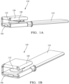
- the electrical connector 110 includes a contact button 112 that is attached to a first electrical bus bar 114 formed of an electrically conductive material, such as a copper-based or aluminum-based material.
- the contact button 112 may be attached to the first bus bar 114 by brazing, soldering, resistance welding, laser welding, spin welding or any other suitable process.
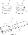
- the contact button 112 has a bottom layer 116 that is attached directly to the first bus bar 114. As illustrated in Fig. 2A , this bottom layer 116 is formed of a first electrically conductive material, such as copper or aluminum.
- the bottom layer 116 may also include a flux material applied over the surface that is to be attached to the first bus bar 114 when using a brazing or welding process.
- the contact button 112 also has a top layer 118 that is formed of a second electrically conductive material and is clad to the bottom layer 116. As illustrated in Fig. 2B , the contact button 112 may also have another intermediate layer 120 between the bottom and top layers 116, 118 that is formed of a third electrically conductive material, e.g., a nickel-based alloy, a steel alloy, a MONEL ® alloy, or a nickel-plated steel alloy. When the contact button 112 includes this intermediate layer 120, the bottom and top layers 116, 118 are clad to the intermediate layer 120.
- the second electrically conductive material is typically different from the first electrically conductive material and preferably has a lower electrical resistance than the first electrically conductive material.
- the second electrically conductive material may be a fine silver, i.e., a silver alloy having 99.9% by weight, a silver-copper alloy, a silver-tin oxide composite material, a silver-carbon composite material , a silver-nickel composite, or a silver-cadmium oxide composite material.
- Contact buttons of this type are available from Umicore Electrical Material USA Inc. of Glen Falls, New York.
- the first bus bar 114 may include a countersunk area 122 or a similar feature to help locate the contact button 112 on the first bus bar 114.
- the electrical connector 110 also includes a clamp assembly 124 having a retaining band 126 that surrounds the contact button 112 and the first bus bar 114.
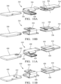
- the clamp assembly 124 also has a spring 128 that is configured to provide a contact force between the contact button 112 and a second electrical bus bar 130 or male blade terminal, shown in Fig. 4 , when the second bus bar 130 or terminal is disposed between the contact button 112 and the spring 128, as shown in Fig. 5 .
- the spring 128 is a cantilevered plate having an arcuate shape that is integrally formed with the retaining band 126.
- the clamp assembly 124 may be formed of a stainless-steel alloy, such as SAE 301 1 ⁇ 2 hard stainless-steel. In alternative embodiments, other spring shapes or materials may be employed to provide the clamping force. It is appreciated that in an alternative embodiment the contact button 112 could be attached to the second electrical bus bar 130.
- the contact button 112 has a generally flat cylindrical shape and the outer edges of the top layer 118 are chamfered as can be seen in Fig. 6 , preferably by a coining process, in order to reduce edges that could increase the mating force when the second bus bar 130 is placed between the spring 128 and the contact button 112.
- the alloy forming the top layer 118 is selected to withstand at least fifty or more mating/unmating cycles between the first and second bus bars 114, 130. Because the top layer 118 is clad to the contact button 112, the thickness of the top layer 118 can be made thicker more economically than providing a plated layer of similar thickness on the contact surface of a bus bar.
- a silver-graphene alloy or other silver-carbon composites having graphene, graphite, or other small carbon particles may be deposited on a surface of the contact button 112 to further increase durability of the electrical connector, thereby providing an increased number of successful mating/unmating cycles.
- alternative embodiments of the contact button 112 may include a number of contact protrusions in the form of spherical bumps 132.
- the bumps 132 provide smaller, more precise geometry than can be formed in thicker bus bars or terminals. This allows for more points of contact in a given area which makes for a more robust interface in a single contact button.
- a number of separate contacts buttons 112 may be arranged and attached to the first bus bar 114 in order to provide more points of contact in a given area.
- the contact buttons 112 may be arranged in a triangular shape to minimize the contact force needed to mate the second bus bar 130 with the electrical connector 110.
- the first bus bar 114 may also include an insulation layer 134 surrounding a portion of the first bus bar 114.
- the electrical connector 210 includes a first bus bar 214 that is formed of parallel first and second layers 236, 238 of electrically conductive material.
- the first and second layers 236, 238 are mechanically and electrically joined, for example by welding, riveting, use of a clinch pin, etc. Ends of the first and second layers 236, 238 are separated so that a second electrical bus bar 230 may be received between them.
- a contact button 212 is attached to the second layer 238 of the first bus bar 214, which in this embodiment is thicker than the first layer 236 of the first bus bar 214.
- the electrical connector 210 also includes a clamp assembly 224 having a retaining band 226 that surrounds the contact buttons 212 and the first bus bar 214.
- the clamp assembly 224 also has a spring 228 that is configured to provide a contact force between the contact button 212 on the first bus bar 214 and the second electrical bus bar 230 by pressing against the first bus bar 214 which then presses the contact button 212 against the second bus bar 230.
- FIG. 10A and 10B Another alternative embodiment of an electrical connector 310 is shown in Figs. 10A and 10B .
- the electrical connector 310 is similar to the electrical connector 210 shown in Fig. 9 , with a primary difference being the contact button 312 is attached to the second electrical bus bar 330 rather than to the second layer 338 of the first bus bar 314.
- the electrical connector 310 also includes a clamp assembly 324 having a retaining band 326 that surrounds the contact buttons 312 and the first bus bar 314.
- the clamp assembly 324 also has a spring 328 that is configured to provide a contact force between the contact button 312 on the second bus bar 330 and the first bus bar 314.
- FIGs. 11A and 11B Yet another alternative embodiment of an electrical connector 410 is shown in Figs. 11A and 11B .
- the electrical connector 410 is similar to the electrical connector 210 shown in Fig. 9 , with a primary difference being the parallel first and second layers 436, 438 of the first bus bar 414 have the same thickness and are symmetrically arranged in relation to a joint 440 between them.
- Contact buttons 412 are attached to the upper and lower surfaces the second bus bar 430.
- the electrical connector 410 also includes a clamp assembly 424 having a retaining band 426 that surrounds the contact button 412 and the first bus bar 414.
- the clamp assembly 424 also has a spring 428 that is configured to provide a contact force between the contact button 412 on the first bus bar 414 and the second bus bar 430 by pressing against the first bus bar 414 which then presses the contact button 412 against the second bus bar 430.
- Fig. 12 shows a flow chart of a method 500 of forming an electrical connector configured to interconnect two electrical bus bars. The method includes the following steps:
- 'one or more' includes a function being performed by one element, a function being performed by more than one element, e.g., in a distributed fashion, several functions being performed by one element, several functions being performed by several elements, or any combination of the above.
- first, second, etc. are, in some instances, used herein to describe various elements, these elements should not be limited by these terms. These terms are only used to distinguish one element from another.
- a first contact could be termed a second contact, and, similarly, a second contact could be termed a first contact, without departing from the scope of the various described embodiments.
- the first contact and the second contact are both contacts, but they are not the same contact.
- the term “if' is, optionally, construed to mean “when” or “upon” or “in response to determining” or “in response to detecting,” depending on the context.
- the phrase “if it is determined” or “if [a stated condition or event] is detected” is, optionally, construed to mean “upon determining” or “in response to determining” or “upon detecting [the stated condition or event]” or “in response to detecting [the stated condition or event],” depending on the context.
Landscapes
- Coupling Device And Connection With Printed Circuit (AREA)
- Connections Effected By Soldering, Adhesion, Or Permanent Deformation (AREA)
- Multi-Conductor Connections (AREA)
Claims (15)
- Elektrischer Verbinder (110), umfassend:einen Kontaktknopf (112) undeine Klemmbaugruppe (124), die ein Halteband (126) beinhaltet, das den Kontaktknopf (112) und eine erste elektrische Sammelschiene (114) umgibt, und eine Feder (128) aufweist, die dazu konfiguriert ist, eine Kontaktkraft zwischen dem Kontaktknopf (112) und einer zweiten elektrischen Sammelschiene (130) bereitzustellen, wenn die zweite elektrische Sammelschiene (130) zwischen dem Kontaktknopf (112) und der Feder (28) angeordnet ist; wobei der Verbinder dadurch gekennzeichnet ist, dass der Kontaktknopf (112) eine erste Schicht (116) aufweist, die aus einem ersten elektrisch leitenden Material gebildet ist und an der ersten elektrischen Sammelschiene (114) angebracht ist, und eine zweite Schicht (118) aufweist, die aus einem zweiten elektrisch leitenden Material gebildet ist und auf die erste Schicht (116) aufgebracht ist.
- Elektrischer Verbinder (110) nach Anspruch 1, wobei eine Außenfläche der zweiten Schicht eine Vielzahl von Vorsprüngen (132) definiert.
- Elektrischer Verbinder (110) nach Anspruch 2, wobei die Vielzahl von Vorsprüngen (132) in Form einer Vielzahl von Kugelabschnitten vorliegt.
- Elektrischer Verbinder (110) nach einem der vorhergehenden Ansprüche, wobei der Kontaktknopf (112) eine allgemein zylindrische Form aufweist.
- Elektrischer Verbinder (110) nach Anspruch 4, wobei eine Kante der zweiten Schicht (118) abgeschrägt ist.
- Elektrischer Verbinder (110) nach einem der vorhergehenden Ansprüche, wobei das zweite elektrisch leitende Material aus einer Liste ausgewählt ist, die aus Feinsilber, einer Silber-Kupfer-Legierung, einem Silber-Zinnoxid-Verbundmaterial, einem Silber-Kohlenstoff-Verbundwerkstoff, einem Silber-Nickel-Verbundwerkstoff und einem Silber-Cadmiumoxid-Verbundmaterial besteht.
- Elektrischer Verbinder (110) nach einem der vorhergehenden Ansprüche, umfassend eine Vielzahl von Kontaktknöpfen (112).
- Elektrischer Verbinder (110) nach Anspruch 7, wobei die Vielzahl von Kontaktknöpfen (112) in einem dreieckigen Muster angeordnet ist.
- Elektrischer Verbinder (210, 310) nach einem der vorhergehenden Ansprüche, wobei die erste Sammelschiene (214, 314) aus einer mechanisch und elektrisch verbundenen parallelen ersten und zweiten Schicht (236, 238, 336, 338) aus elektrisch leitendem Material gebildet ist, und wobei Enden der ersten und der zweiten Schicht (236, 238, 336, 338) der ersten Sammelschiene (214, 314) getrennt sind, sodass die zweite elektrische Sammelschiene (230, 330) zwischen ihnen aufgenommen werden kann.
- Elektrischer Verbinder (410) nach Anspruch 9, wobei die erste und die zweite Schicht (436, 438) der ersten Sammelschiene (414) symmetrisch zu einer Verbindungsstelle (440) zwischen ihnen sind.
- Verfahren (500) zum Bilden eines elektrischen Verbinders (110), der zum Verbinden zweier elektrischer Sammelschienen (114, 130) miteinander konfiguriert ist, umfassend:Anbringen (502) eines Kontaktknopfes (112) an einer ersten elektrischen Sammelschiene (114), wobei der Kontaktknopf (112) eine erste Schicht (116) aus einem ersten elektrisch leitenden Material und eine zweite Schicht (118) aus einem zweiten elektrisch leitenden Material aufweist, das auf die erste Schicht (116) aufgebracht ist; undAnbringen (504) einer Klemmbaugruppe (124), die ein Halteband (126) beinhaltet, an der ersten elektrischen Sammelschiene (114), derart, dass die Klemmbaugruppe (124) den Kontaktknopf (112) und die erste elektrische Sammelschiene (114) umgibt, wobei die Klemmbaugruppe (124) eine Feder (128) aufweist, die dazu konfiguriert ist, eine Kontaktkraft zwischen dem Kontaktknopf (112) und einer zweiten elektrischen Sammelschiene (130) bereitzustellen, wenn eine zweite elektrische Sammelschiene (130) zwischen dem Kontaktknopf (112) und der Feder (128) angeordnet ist.
- Verfahren (500) nach Anspruch 11, wobei der Kontaktknopf (112) an der ersten elektrischen Sammelschiene (114) durch einen Prozess angebracht wird, der aus Hartlöten, Weichlöten, Widerstandsschweißen, Laserschweißen und Rotationsschweißen ausgewählt wird.
- Verfahren (500) nach Anspruch 11 oder 12, ferner umfassend Anbringen (506) einer Vielzahl von Kontaktknöpfen (112) an der ersten elektrischen Sammelschiene (114).
- Verfahren (500) nach einem der Ansprüche 11 bis 13, wobei die erste Sammelschiene (214, 314) aus einer mechanisch und elektrisch verbundenen parallelen ersten und zweiten Schicht (236, 238, 336, 338) aus elektrisch leitendem Material gebildet wird, wobei Enden der ersten und der zweiten Schicht (236, 238, 336, 338) der ersten Sammelschiene (214, 314) getrennt werden, und wobei das Verfahren ferner Einführen (510) der zweiten elektrischen Sammelschiene (230, 330) zwischen den Enden der ersten und der zweiten Schicht (236, 238, 336, 338) der ersten Sammelschiene (214, 314) beinhaltet.
- Elektrischer Verbinder (500) nach Anspruch 14, wobei die erste und die zweite Schicht (436, 438) der ersten Sammelschiene (414) symmetrisch zu einer Verbindungsstelle (440) zwischen ihnen sind.
Priority Applications (2)
| Application Number | Priority Date | Filing Date | Title |
|---|---|---|---|
| EP24205484.9A EP4468524B1 (de) | 2021-08-16 | 2022-08-12 | Elektrischer hochspannungsverbinder mit plattiertem kontaktknopf und verfahren zu seiner herstellung |
| EP23197633.3A EP4270670B1 (de) | 2021-08-16 | 2022-08-12 | Elektrischer hochspannungsverbinder mit plattiertem kontaktknopf und verfahren zu seiner herstellung |
Applications Claiming Priority (2)
| Application Number | Priority Date | Filing Date | Title |
|---|---|---|---|
| US202163233382P | 2021-08-16 | 2021-08-16 | |
| US17/884,886 US20230049062A1 (en) | 2021-08-16 | 2022-08-10 | High voltage electrical connector with clad contact button and method of manufacturing same |
Related Child Applications (2)
| Application Number | Title | Priority Date | Filing Date |
|---|---|---|---|
| EP23197633.3A Division EP4270670B1 (de) | 2021-08-16 | 2022-08-12 | Elektrischer hochspannungsverbinder mit plattiertem kontaktknopf und verfahren zu seiner herstellung |
| EP24205484.9A Division EP4468524B1 (de) | 2021-08-16 | 2022-08-12 | Elektrischer hochspannungsverbinder mit plattiertem kontaktknopf und verfahren zu seiner herstellung |
Publications (2)
| Publication Number | Publication Date |
|---|---|
| EP4138224A1 EP4138224A1 (de) | 2023-02-22 |
| EP4138224B1 true EP4138224B1 (de) | 2023-09-27 |
Family
ID=82932725
Family Applications (3)
| Application Number | Title | Priority Date | Filing Date |
|---|---|---|---|
| EP24205484.9A Active EP4468524B1 (de) | 2021-08-16 | 2022-08-12 | Elektrischer hochspannungsverbinder mit plattiertem kontaktknopf und verfahren zu seiner herstellung |
| EP22190196.0A Active EP4138224B1 (de) | 2021-08-16 | 2022-08-12 | Elektrischer hochspannungsverbinder mit plattiertem kontaktknopf und verfahren zu seiner herstellung |
| EP23197633.3A Active EP4270670B1 (de) | 2021-08-16 | 2022-08-12 | Elektrischer hochspannungsverbinder mit plattiertem kontaktknopf und verfahren zu seiner herstellung |
Family Applications Before (1)
| Application Number | Title | Priority Date | Filing Date |
|---|---|---|---|
| EP24205484.9A Active EP4468524B1 (de) | 2021-08-16 | 2022-08-12 | Elektrischer hochspannungsverbinder mit plattiertem kontaktknopf und verfahren zu seiner herstellung |
Family Applications After (1)
| Application Number | Title | Priority Date | Filing Date |
|---|---|---|---|
| EP23197633.3A Active EP4270670B1 (de) | 2021-08-16 | 2022-08-12 | Elektrischer hochspannungsverbinder mit plattiertem kontaktknopf und verfahren zu seiner herstellung |
Country Status (3)
| Country | Link |
|---|---|
| US (2) | US20230049062A1 (de) |
| EP (3) | EP4468524B1 (de) |
| CN (1) | CN115706351A (de) |
Family Cites Families (15)
| Publication number | Priority date | Publication date | Assignee | Title |
|---|---|---|---|---|
| US4273409A (en) * | 1979-09-04 | 1981-06-16 | Victor Electric Wire & Cable | Connector having low profile contact element |
| US5235743A (en) * | 1990-07-11 | 1993-08-17 | Yazaki Corporation | Method of manufacturing a pair of terminals having a low friction material on a mating surface to facilitate connection of the terminals |
| KR970707616A (ko) * | 1995-08-18 | 1997-12-01 | 이케다 테루타카 | 자동차용 커넥터플러그(connector plug for automobiles) |
| US11266014B2 (en) * | 2008-02-14 | 2022-03-01 | Metrospec Technology, L.L.C. | LED lighting systems and method |
| KR100867415B1 (ko) * | 2008-04-16 | 2008-11-06 | 주식회사 네오스코 | 코인형 진동모터의 정류자 구조체 |
| JP5760060B2 (ja) * | 2013-09-27 | 2015-08-05 | 株式会社茨城技研 | 金属皮膜形成方法並びに金属皮膜形成製品の製造方法及び製造装置 |
| US9627804B2 (en) * | 2014-12-19 | 2017-04-18 | Intel Corporation | Snap button fastener providing electrical connection |
| CN204720608U (zh) * | 2015-05-19 | 2015-10-21 | 乐清市合达电子有限公司 | 纽扣端子 |
| CN106450863B (zh) * | 2016-09-28 | 2019-05-07 | 佛山市顺德区依士文电子仪器有限公司 | 电极片 |
| US10741955B2 (en) * | 2016-09-29 | 2020-08-11 | Veoneer Us, Inc. | Sensor assembly and method for assembling a sensor connector assembly |
| US10640232B2 (en) * | 2016-12-20 | 2020-05-05 | The Boeing Company | Conductive fastening system for composite structures |
| WO2019142459A1 (ja) * | 2018-01-16 | 2019-07-25 | 株式会社オートネットワーク技術研究所 | 端子 |
| US10389055B1 (en) * | 2018-06-20 | 2019-08-20 | Delphia Technologies, Llc | Electrical connector assembly |
| CN209730345U (zh) * | 2019-05-21 | 2019-12-03 | 伍友诚 | 一种公端插头接口 |
| CN117913571A (zh) * | 2020-12-30 | 2024-04-19 | 泰科电子(上海)有限公司 | 端子组件和连接器 |
-
2022
- 2022-08-10 US US17/884,886 patent/US20230049062A1/en not_active Abandoned
- 2022-08-12 EP EP24205484.9A patent/EP4468524B1/de active Active
- 2022-08-12 EP EP22190196.0A patent/EP4138224B1/de active Active
- 2022-08-12 EP EP23197633.3A patent/EP4270670B1/de active Active
- 2022-08-15 CN CN202210974695.8A patent/CN115706351A/zh active Pending
-
2025
- 2025-09-05 US US19/320,427 patent/US20260005450A1/en active Pending
Also Published As
| Publication number | Publication date |
|---|---|
| CN115706351A (zh) | 2023-02-17 |
| EP4468524A3 (de) | 2025-02-19 |
| EP4138224A1 (de) | 2023-02-22 |
| EP4468524A2 (de) | 2024-11-27 |
| EP4468524B1 (de) | 2025-12-03 |
| EP4270670A3 (de) | 2024-01-17 |
| US20230049062A1 (en) | 2023-02-16 |
| EP4270670B1 (de) | 2024-11-06 |
| EP4270670A2 (de) | 2023-11-01 |
| US20260005450A1 (en) | 2026-01-01 |
Similar Documents
| Publication | Publication Date | Title |
|---|---|---|
| US10230191B2 (en) | High-current electrical connector with multi-point contact spring | |
| KR102249177B1 (ko) | 클램핑력이 향상된 전기 단자 | |
| US5139427A (en) | Planar array connector and flexible contact therefor | |
| US20070123084A1 (en) | Electric contact and female terminal | |
| CN1725560B (zh) | 连接电导线的接线柱 | |
| KR101690894B1 (ko) | 전기 컨택트 어셈블리 | |
| CN102034656A (zh) | 具有可扩展性的高功率保险丝端子 | |
| JPH0883661A (ja) | 電気コネクター | |
| CN109616808B (zh) | 大电流电连接器 | |
| JP6623853B2 (ja) | コンタクトの接触構造 | |
| WO2013023134A1 (en) | Curved spring beam having coined indentations | |
| WO2001022457A1 (en) | Low current high temperature switch contacts | |
| EP4138224B1 (de) | Elektrischer hochspannungsverbinder mit plattiertem kontaktknopf und verfahren zu seiner herstellung | |
| CN107026338A (zh) | 端子对及连接器 | |
| JP2003086278A (ja) | 高電圧用端子 | |
| JP2021093345A (ja) | プレスフィット端子、プレスフィット端子付基板及び機器 | |
| US20260104437A1 (en) | Probe for probe card | |
| JP2974704B2 (ja) | チェンジ・オーバコンタクトリレー用の接点装置 | |
| CN112912986B (zh) | 保护元件 | |
| US10446944B1 (en) | Devices, systems, and methods for increasing terminal electrical contact | |
| EP4683118A1 (de) | Elektrischer leiter mit folienkontakt auf einer ebenen oberfläche und verfahren zu seiner herstellung | |
| JP3473475B2 (ja) | 車両電装品用の接続端子 | |
| WO2021106546A1 (ja) | プレスフィット端子、プレスフィット端子付基板及び機器 | |
| CN213277832U (zh) | 开关触头及开关触头结构 | |
| EP3803927B1 (de) | Verfahren zum anbringen von kontakten auf leitern aus aluminium in einer elektrischen schaltvorrichtung |
Legal Events
| Date | Code | Title | Description |
|---|---|---|---|
| PUAI | Public reference made under article 153(3) epc to a published international application that has entered the european phase |
Free format text: ORIGINAL CODE: 0009012 |
|
| STAA | Information on the status of an ep patent application or granted ep patent |
Free format text: STATUS: THE APPLICATION HAS BEEN PUBLISHED |
|
| AK | Designated contracting states |
Kind code of ref document: A1 Designated state(s): AL AT BE BG CH CY CZ DE DK EE ES FI FR GB GR HR HU IE IS IT LI LT LU LV MC MK MT NL NO PL PT RO RS SE SI SK SM TR |
|
| STAA | Information on the status of an ep patent application or granted ep patent |
Free format text: STATUS: REQUEST FOR EXAMINATION WAS MADE |
|
| 17P | Request for examination filed |
Effective date: 20230220 |
|
| RAP3 | Party data changed (applicant data changed or rights of an application transferred) |
Owner name: APTIV TECHNOLOGIES LIMITED |
|
| RBV | Designated contracting states (corrected) |
Designated state(s): AL AT BE BG CH CY CZ DE DK EE ES FI FR GB GR HR HU IE IS IT LI LT LU LV MC MK MT NL NO PL PT RO RS SE SI SK SM TR |
|
| GRAP | Despatch of communication of intention to grant a patent |
Free format text: ORIGINAL CODE: EPIDOSNIGR1 |
|
| STAA | Information on the status of an ep patent application or granted ep patent |
Free format text: STATUS: GRANT OF PATENT IS INTENDED |
|
| RIC1 | Information provided on ipc code assigned before grant |
Ipc: H01R 43/16 20060101ALN20230627BHEP Ipc: H01R 13/03 20060101ALI20230627BHEP Ipc: H01R 13/187 20060101AFI20230627BHEP |
|
| INTG | Intention to grant announced |
Effective date: 20230717 |
|
| GRAS | Grant fee paid |
Free format text: ORIGINAL CODE: EPIDOSNIGR3 |
|
| GRAA | (expected) grant |
Free format text: ORIGINAL CODE: 0009210 |
|
| STAA | Information on the status of an ep patent application or granted ep patent |
Free format text: STATUS: THE PATENT HAS BEEN GRANTED |
|
| P01 | Opt-out of the competence of the unified patent court (upc) registered |
Effective date: 20230803 |
|
| AK | Designated contracting states |
Kind code of ref document: B1 Designated state(s): AL AT BE BG CH CY CZ DE DK EE ES FI FR GB GR HR HU IE IS IT LI LT LU LV MC MK MT NL NO PL PT RO RS SE SI SK SM TR |
|
| REG | Reference to a national code |
Ref country code: GB Ref legal event code: FG4D |
|
| REG | Reference to a national code |
Ref country code: CH Ref legal event code: EP |
|
| REG | Reference to a national code |
Ref country code: DE Ref legal event code: R096 Ref document number: 602022000573 Country of ref document: DE |
|
| REG | Reference to a national code |
Ref country code: IE Ref legal event code: FG4D |
|
| REG | Reference to a national code |
Ref country code: LT Ref legal event code: MG9D |
|
| PG25 | Lapsed in a contracting state [announced via postgrant information from national office to epo] |
Ref country code: GR Free format text: LAPSE BECAUSE OF FAILURE TO SUBMIT A TRANSLATION OF THE DESCRIPTION OR TO PAY THE FEE WITHIN THE PRESCRIBED TIME-LIMIT Effective date: 20231228 |
|
| PG25 | Lapsed in a contracting state [announced via postgrant information from national office to epo] |
Ref country code: SE Free format text: LAPSE BECAUSE OF FAILURE TO SUBMIT A TRANSLATION OF THE DESCRIPTION OR TO PAY THE FEE WITHIN THE PRESCRIBED TIME-LIMIT Effective date: 20230927 Ref country code: RS Free format text: LAPSE BECAUSE OF FAILURE TO SUBMIT A TRANSLATION OF THE DESCRIPTION OR TO PAY THE FEE WITHIN THE PRESCRIBED TIME-LIMIT Effective date: 20230927 Ref country code: NO Free format text: LAPSE BECAUSE OF FAILURE TO SUBMIT A TRANSLATION OF THE DESCRIPTION OR TO PAY THE FEE WITHIN THE PRESCRIBED TIME-LIMIT Effective date: 20231227 Ref country code: LV Free format text: LAPSE BECAUSE OF FAILURE TO SUBMIT A TRANSLATION OF THE DESCRIPTION OR TO PAY THE FEE WITHIN THE PRESCRIBED TIME-LIMIT Effective date: 20230927 Ref country code: LT Free format text: LAPSE BECAUSE OF FAILURE TO SUBMIT A TRANSLATION OF THE DESCRIPTION OR TO PAY THE FEE WITHIN THE PRESCRIBED TIME-LIMIT Effective date: 20230927 Ref country code: HR Free format text: LAPSE BECAUSE OF FAILURE TO SUBMIT A TRANSLATION OF THE DESCRIPTION OR TO PAY THE FEE WITHIN THE PRESCRIBED TIME-LIMIT Effective date: 20230927 Ref country code: GR Free format text: LAPSE BECAUSE OF FAILURE TO SUBMIT A TRANSLATION OF THE DESCRIPTION OR TO PAY THE FEE WITHIN THE PRESCRIBED TIME-LIMIT Effective date: 20231228 Ref country code: FI Free format text: LAPSE BECAUSE OF FAILURE TO SUBMIT A TRANSLATION OF THE DESCRIPTION OR TO PAY THE FEE WITHIN THE PRESCRIBED TIME-LIMIT Effective date: 20230927 |
|
| REG | Reference to a national code |
Ref country code: NL Ref legal event code: MP Effective date: 20230927 |
|
| REG | Reference to a national code |
Ref country code: AT Ref legal event code: MK05 Ref document number: 1616348 Country of ref document: AT Kind code of ref document: T Effective date: 20230927 |
|
| PG25 | Lapsed in a contracting state [announced via postgrant information from national office to epo] |
Ref country code: NL Free format text: LAPSE BECAUSE OF FAILURE TO SUBMIT A TRANSLATION OF THE DESCRIPTION OR TO PAY THE FEE WITHIN THE PRESCRIBED TIME-LIMIT Effective date: 20230927 |
|
| PG25 | Lapsed in a contracting state [announced via postgrant information from national office to epo] |
Ref country code: IS Free format text: LAPSE BECAUSE OF FAILURE TO SUBMIT A TRANSLATION OF THE DESCRIPTION OR TO PAY THE FEE WITHIN THE PRESCRIBED TIME-LIMIT Effective date: 20240127 |
|
| PG25 | Lapsed in a contracting state [announced via postgrant information from national office to epo] |
Ref country code: AT Free format text: LAPSE BECAUSE OF FAILURE TO SUBMIT A TRANSLATION OF THE DESCRIPTION OR TO PAY THE FEE WITHIN THE PRESCRIBED TIME-LIMIT Effective date: 20230927 |
|
| PG25 | Lapsed in a contracting state [announced via postgrant information from national office to epo] |
Ref country code: ES Free format text: LAPSE BECAUSE OF FAILURE TO SUBMIT A TRANSLATION OF THE DESCRIPTION OR TO PAY THE FEE WITHIN THE PRESCRIBED TIME-LIMIT Effective date: 20230927 |
|
| PG25 | Lapsed in a contracting state [announced via postgrant information from national office to epo] |
Ref country code: SM Free format text: LAPSE BECAUSE OF FAILURE TO SUBMIT A TRANSLATION OF THE DESCRIPTION OR TO PAY THE FEE WITHIN THE PRESCRIBED TIME-LIMIT Effective date: 20230927 Ref country code: RO Free format text: LAPSE BECAUSE OF FAILURE TO SUBMIT A TRANSLATION OF THE DESCRIPTION OR TO PAY THE FEE WITHIN THE PRESCRIBED TIME-LIMIT Effective date: 20230927 Ref country code: IS Free format text: LAPSE BECAUSE OF FAILURE TO SUBMIT A TRANSLATION OF THE DESCRIPTION OR TO PAY THE FEE WITHIN THE PRESCRIBED TIME-LIMIT Effective date: 20240127 Ref country code: ES Free format text: LAPSE BECAUSE OF FAILURE TO SUBMIT A TRANSLATION OF THE DESCRIPTION OR TO PAY THE FEE WITHIN THE PRESCRIBED TIME-LIMIT Effective date: 20230927 Ref country code: EE Free format text: LAPSE BECAUSE OF FAILURE TO SUBMIT A TRANSLATION OF THE DESCRIPTION OR TO PAY THE FEE WITHIN THE PRESCRIBED TIME-LIMIT Effective date: 20230927 Ref country code: CZ Free format text: LAPSE BECAUSE OF FAILURE TO SUBMIT A TRANSLATION OF THE DESCRIPTION OR TO PAY THE FEE WITHIN THE PRESCRIBED TIME-LIMIT Effective date: 20230927 Ref country code: AT Free format text: LAPSE BECAUSE OF FAILURE TO SUBMIT A TRANSLATION OF THE DESCRIPTION OR TO PAY THE FEE WITHIN THE PRESCRIBED TIME-LIMIT Effective date: 20230927 Ref country code: SK Free format text: LAPSE BECAUSE OF FAILURE TO SUBMIT A TRANSLATION OF THE DESCRIPTION OR TO PAY THE FEE WITHIN THE PRESCRIBED TIME-LIMIT Effective date: 20230927 Ref country code: PT Free format text: LAPSE BECAUSE OF FAILURE TO SUBMIT A TRANSLATION OF THE DESCRIPTION OR TO PAY THE FEE WITHIN THE PRESCRIBED TIME-LIMIT Effective date: 20240129 |
|
| PG25 | Lapsed in a contracting state [announced via postgrant information from national office to epo] |
Ref country code: PL Free format text: LAPSE BECAUSE OF FAILURE TO SUBMIT A TRANSLATION OF THE DESCRIPTION OR TO PAY THE FEE WITHIN THE PRESCRIBED TIME-LIMIT Effective date: 20230927 Ref country code: IT Free format text: LAPSE BECAUSE OF FAILURE TO SUBMIT A TRANSLATION OF THE DESCRIPTION OR TO PAY THE FEE WITHIN THE PRESCRIBED TIME-LIMIT Effective date: 20230927 |
|
| REG | Reference to a national code |
Ref country code: DE Ref legal event code: R097 Ref document number: 602022000573 Country of ref document: DE |
|
| PG25 | Lapsed in a contracting state [announced via postgrant information from national office to epo] |
Ref country code: DK Free format text: LAPSE BECAUSE OF FAILURE TO SUBMIT A TRANSLATION OF THE DESCRIPTION OR TO PAY THE FEE WITHIN THE PRESCRIBED TIME-LIMIT Effective date: 20230927 |
|
| PG25 | Lapsed in a contracting state [announced via postgrant information from national office to epo] |
Ref country code: DK Free format text: LAPSE BECAUSE OF FAILURE TO SUBMIT A TRANSLATION OF THE DESCRIPTION OR TO PAY THE FEE WITHIN THE PRESCRIBED TIME-LIMIT Effective date: 20230927 |
|
| PLBE | No opposition filed within time limit |
Free format text: ORIGINAL CODE: 0009261 |
|
| STAA | Information on the status of an ep patent application or granted ep patent |
Free format text: STATUS: NO OPPOSITION FILED WITHIN TIME LIMIT |
|
| 26N | No opposition filed |
Effective date: 20240628 |
|
| PG25 | Lapsed in a contracting state [announced via postgrant information from national office to epo] |
Ref country code: SI Free format text: LAPSE BECAUSE OF FAILURE TO SUBMIT A TRANSLATION OF THE DESCRIPTION OR TO PAY THE FEE WITHIN THE PRESCRIBED TIME-LIMIT Effective date: 20230927 |
|
| PG25 | Lapsed in a contracting state [announced via postgrant information from national office to epo] |
Ref country code: SI Free format text: LAPSE BECAUSE OF FAILURE TO SUBMIT A TRANSLATION OF THE DESCRIPTION OR TO PAY THE FEE WITHIN THE PRESCRIBED TIME-LIMIT Effective date: 20230927 |
|
| PG25 | Lapsed in a contracting state [announced via postgrant information from national office to epo] |
Ref country code: BG Free format text: LAPSE BECAUSE OF FAILURE TO SUBMIT A TRANSLATION OF THE DESCRIPTION OR TO PAY THE FEE WITHIN THE PRESCRIBED TIME-LIMIT Effective date: 20230927 |
|
| PG25 | Lapsed in a contracting state [announced via postgrant information from national office to epo] |
Ref country code: BG Free format text: LAPSE BECAUSE OF FAILURE TO SUBMIT A TRANSLATION OF THE DESCRIPTION OR TO PAY THE FEE WITHIN THE PRESCRIBED TIME-LIMIT Effective date: 20230927 |
|
| PG25 | Lapsed in a contracting state [announced via postgrant information from national office to epo] |
Ref country code: LU Free format text: LAPSE BECAUSE OF NON-PAYMENT OF DUE FEES Effective date: 20240812 |
|
| PG25 | Lapsed in a contracting state [announced via postgrant information from national office to epo] |
Ref country code: MC Free format text: LAPSE BECAUSE OF FAILURE TO SUBMIT A TRANSLATION OF THE DESCRIPTION OR TO PAY THE FEE WITHIN THE PRESCRIBED TIME-LIMIT Effective date: 20230927 |
|
| REG | Reference to a national code |
Ref country code: BE Ref legal event code: MM Effective date: 20240831 |
|
| PG25 | Lapsed in a contracting state [announced via postgrant information from national office to epo] |
Ref country code: BE Free format text: LAPSE BECAUSE OF NON-PAYMENT OF DUE FEES Effective date: 20240831 |
|
| PG25 | Lapsed in a contracting state [announced via postgrant information from national office to epo] |
Ref country code: IE Free format text: LAPSE BECAUSE OF NON-PAYMENT OF DUE FEES Effective date: 20240812 |
|
| PGFP | Annual fee paid to national office [announced via postgrant information from national office to epo] |
Ref country code: DE Payment date: 20250722 Year of fee payment: 4 |
|
| PGFP | Annual fee paid to national office [announced via postgrant information from national office to epo] |
Ref country code: FR Payment date: 20250703 Year of fee payment: 4 |
|
| PG25 | Lapsed in a contracting state [announced via postgrant information from national office to epo] |
Ref country code: CY Free format text: LAPSE BECAUSE OF FAILURE TO SUBMIT A TRANSLATION OF THE DESCRIPTION OR TO PAY THE FEE WITHIN THE PRESCRIBED TIME-LIMIT; INVALID AB INITIO Effective date: 20220812 |
|
| PG25 | Lapsed in a contracting state [announced via postgrant information from national office to epo] |
Ref country code: HU Free format text: LAPSE BECAUSE OF FAILURE TO SUBMIT A TRANSLATION OF THE DESCRIPTION OR TO PAY THE FEE WITHIN THE PRESCRIBED TIME-LIMIT; INVALID AB INITIO Effective date: 20220812 |
|
| REG | Reference to a national code |
Ref country code: CH Ref legal event code: H13 Free format text: ST27 STATUS EVENT CODE: U-0-0-H10-H13 (AS PROVIDED BY THE NATIONAL OFFICE) Effective date: 20260324 |
|
| PG25 | Lapsed in a contracting state [announced via postgrant information from national office to epo] |
Ref country code: CH Free format text: LAPSE BECAUSE OF NON-PAYMENT OF DUE FEES Effective date: 20250831 |