EP4141497A1 - Capteur optoélectronique et procédé de détection des objets dans une zone de surveillance - Google Patents
Capteur optoélectronique et procédé de détection des objets dans une zone de surveillance Download PDFInfo
- Publication number
- EP4141497A1 EP4141497A1 EP22189435.5A EP22189435A EP4141497A1 EP 4141497 A1 EP4141497 A1 EP 4141497A1 EP 22189435 A EP22189435 A EP 22189435A EP 4141497 A1 EP4141497 A1 EP 4141497A1
- Authority
- EP
- European Patent Office
- Prior art keywords
- sensor
- light
- meta
- optical
- distance
- Prior art date
- Legal status (The legal status is an assumption and is not a legal conclusion. Google has not performed a legal analysis and makes no representation as to the accuracy of the status listed.)
- Withdrawn
Links
- 230000005693 optoelectronics Effects 0.000 title claims abstract description 13
- 238000000034 method Methods 0.000 title claims description 5
- 230000003287 optical effect Effects 0.000 claims abstract description 101
- 230000005540 biological transmission Effects 0.000 claims abstract description 26
- 238000006073 displacement reaction Methods 0.000 claims abstract description 14
- 230000001419 dependent effect Effects 0.000 claims abstract description 13
- 239000000463 material Substances 0.000 claims abstract description 9
- 238000011156 evaluation Methods 0.000 claims abstract description 4
- 238000012937 correction Methods 0.000 claims description 17
- 229910052751 metal Inorganic materials 0.000 claims description 8
- 239000002184 metal Substances 0.000 claims description 8
- 230000004888 barrier function Effects 0.000 claims description 2
- 230000000694 effects Effects 0.000 description 18
- 239000002086 nanomaterial Substances 0.000 description 16
- 238000013461 design Methods 0.000 description 7
- 238000005259 measurement Methods 0.000 description 6
- 238000003384 imaging method Methods 0.000 description 5
- 210000001747 pupil Anatomy 0.000 description 5
- 230000035945 sensitivity Effects 0.000 description 5
- 230000008901 benefit Effects 0.000 description 4
- 230000003247 decreasing effect Effects 0.000 description 4
- 230000009467 reduction Effects 0.000 description 4
- 239000000758 substrate Substances 0.000 description 4
- 239000013589 supplement Substances 0.000 description 4
- 230000000875 corresponding effect Effects 0.000 description 3
- 239000011159 matrix material Substances 0.000 description 3
- GWEVSGVZZGPLCZ-UHFFFAOYSA-N Titan oxide Chemical compound O=[Ti]=O GWEVSGVZZGPLCZ-UHFFFAOYSA-N 0.000 description 2
- 238000010586 diagram Methods 0.000 description 2
- 229910052710 silicon Inorganic materials 0.000 description 2
- 239000010703 silicon Substances 0.000 description 2
- 230000003595 spectral effect Effects 0.000 description 2
- 229910005540 GaP Inorganic materials 0.000 description 1
- 229910052581 Si3N4 Inorganic materials 0.000 description 1
- VYPSYNLAJGMNEJ-UHFFFAOYSA-N Silicium dioxide Chemical compound O=[Si]=O VYPSYNLAJGMNEJ-UHFFFAOYSA-N 0.000 description 1
- 238000004026 adhesive bonding Methods 0.000 description 1
- 229910045601 alloy Inorganic materials 0.000 description 1
- 239000000956 alloy Substances 0.000 description 1
- 238000003491 array Methods 0.000 description 1
- 239000012876 carrier material Substances 0.000 description 1
- 150000004770 chalcogenides Chemical class 0.000 description 1
- 230000008859 change Effects 0.000 description 1
- 238000004891 communication Methods 0.000 description 1
- 230000000295 complement effect Effects 0.000 description 1
- 239000002131 composite material Substances 0.000 description 1
- PMHQVHHXPFUNSP-UHFFFAOYSA-M copper(1+);methylsulfanylmethane;bromide Chemical compound Br[Cu].CSC PMHQVHHXPFUNSP-UHFFFAOYSA-M 0.000 description 1
- 230000007423 decrease Effects 0.000 description 1
- 238000009826 distribution Methods 0.000 description 1
- 230000008030 elimination Effects 0.000 description 1
- 238000003379 elimination reaction Methods 0.000 description 1
- 238000005516 engineering process Methods 0.000 description 1
- HZXMRANICFIONG-UHFFFAOYSA-N gallium phosphide Chemical compound [Ga]#P HZXMRANICFIONG-UHFFFAOYSA-N 0.000 description 1
- 230000006872 improvement Effects 0.000 description 1
- 238000009434 installation Methods 0.000 description 1
- 238000004519 manufacturing process Methods 0.000 description 1
- 238000013507 mapping Methods 0.000 description 1
- 238000013508 migration Methods 0.000 description 1
- 230000005012 migration Effects 0.000 description 1
- 238000012544 monitoring process Methods 0.000 description 1
- 230000010287 polarization Effects 0.000 description 1
- 238000012545 processing Methods 0.000 description 1
- 230000001902 propagating effect Effects 0.000 description 1
- 230000004044 response Effects 0.000 description 1
- HQVNEWCFYHHQES-UHFFFAOYSA-N silicon nitride Chemical compound N12[Si]34N5[Si]62N3[Si]51N64 HQVNEWCFYHHQES-UHFFFAOYSA-N 0.000 description 1
- 229910052814 silicon oxide Inorganic materials 0.000 description 1
- 239000007787 solid Substances 0.000 description 1
- 239000004408 titanium dioxide Substances 0.000 description 1
- 238000012546 transfer Methods 0.000 description 1
Images


Classifications
-
- G—PHYSICS
- G01—MEASURING; TESTING
- G01V—GEOPHYSICS; GRAVITATIONAL MEASUREMENTS; DETECTING MASSES OR OBJECTS; TAGS
- G01V8/00—Prospecting or detecting by optical means
- G01V8/10—Detecting, e.g. by using light barriers
- G01V8/12—Detecting, e.g. by using light barriers using one transmitter and one receiver
-
- G—PHYSICS
- G01—MEASURING; TESTING
- G01S—RADIO DIRECTION-FINDING; RADIO NAVIGATION; DETERMINING DISTANCE OR VELOCITY BY USE OF RADIO WAVES; LOCATING OR PRESENCE-DETECTING BY USE OF THE REFLECTION OR RERADIATION OF RADIO WAVES; ANALOGOUS ARRANGEMENTS USING OTHER WAVES
- G01S17/00—Systems using the reflection or reradiation of electromagnetic waves other than radio waves, e.g. lidar systems
- G01S17/02—Systems using the reflection of electromagnetic waves other than radio waves
- G01S17/04—Systems determining the presence of a target
-
- G—PHYSICS
- G01—MEASURING; TESTING
- G01S—RADIO DIRECTION-FINDING; RADIO NAVIGATION; DETERMINING DISTANCE OR VELOCITY BY USE OF RADIO WAVES; LOCATING OR PRESENCE-DETECTING BY USE OF THE REFLECTION OR RERADIATION OF RADIO WAVES; ANALOGOUS ARRANGEMENTS USING OTHER WAVES
- G01S17/00—Systems using the reflection or reradiation of electromagnetic waves other than radio waves, e.g. lidar systems
- G01S17/02—Systems using the reflection of electromagnetic waves other than radio waves
- G01S17/06—Systems determining position data of a target
- G01S17/08—Systems determining position data of a target for measuring distance only
-
- G—PHYSICS
- G01—MEASURING; TESTING
- G01S—RADIO DIRECTION-FINDING; RADIO NAVIGATION; DETERMINING DISTANCE OR VELOCITY BY USE OF RADIO WAVES; LOCATING OR PRESENCE-DETECTING BY USE OF THE REFLECTION OR RERADIATION OF RADIO WAVES; ANALOGOUS ARRANGEMENTS USING OTHER WAVES
- G01S7/00—Details of systems according to groups G01S13/00, G01S15/00, G01S17/00
- G01S7/48—Details of systems according to groups G01S13/00, G01S15/00, G01S17/00 of systems according to group G01S17/00
- G01S7/481—Constructional features, e.g. arrangements of optical elements
- G01S7/4816—Constructional features, e.g. arrangements of optical elements of receivers alone
-
- G—PHYSICS
- G02—OPTICS
- G02B—OPTICAL ELEMENTS, SYSTEMS OR APPARATUS
- G02B1/00—Optical elements characterised by the material of which they are made; Optical coatings for optical elements
- G02B1/002—Optical elements characterised by the material of which they are made; Optical coatings for optical elements made of materials engineered to provide properties not available in nature, e.g. metamaterials
Definitions
- the invention relates to an optoelectronic sensor and a method for detecting objects in a surveillance area according to the preamble of claim 1 and 15, respectively.
- Photoelectric sensors usually use a receiver lens to focus the light to be detected onto their light receiver.
- Such receiver lenses have a certain size and focal length and this results in a defined distance between the receiver lens and the light receiver.
- the receiving aperture In order to achieve large ranges with a sensor, as much useful light as possible should be collected and the receiving aperture should therefore be large. However, a large reception opening inevitably goes hand in hand with a large installation depth.
- the diameter of the receiving aperture corresponds to the required structural depth for the receiving lens and the light receiver.
- receiving optics with a short focal length can be used
- the parallax caused by the distance between the transmitting and receiving optics can cause the received light spot to migrate from the active area of the light receiver. This is especially true in a work area with a large distance between near and far areas.
- the light energy received or the reception level also decreases approximately quadratically with the object distance.
- the measurement is therefore very sensitive in the close range and very insensitive in the far range.
- the effects described are typically at least partially mitigated by using complex optics with multiple sub-regions or composite optics.
- the EP 0 924 535 B1 , EP 3 018 495 B1 or the EP 3 002 609 B1 by the applicant disclose such solutions, for example.
- Transmitting and receiving optics can, such as in the EP 0 735 501 B1 described, can also be arranged coaxially, with a partially transparent deflection mirror being required in order to get the transmission axis congruent with the reception axis. This results in an additional space requirement for lenses or mirrors. Both solutions are therefore technically complex
- the sensor for example a light sensor or a distance-measuring sensor based on the time-of-flight principle (TOF sensor), has a transmission path in which a light transmitter emits a light beam via a transmission optics and a reception path in which the light beam remitted to an object via a reception optics a light receiver is imaged and a received light spot is generated there, which is detected by the light receiver.
- the remitted light bundle can be created both by diffuse remission and by directed reflection.
- Receiving optics and transmitting optics are offset from one another by a distance, for example measured between the optical axes of the receiving optics and transmitting optics.
- an impact position of the received light spot which the reflected light bundle generates on the light receiver, depends on the distance of the object from the sensor. Since the received light spot is generally not a point with defined edges and has an extension, the position of the received light spot is to be understood below as the position of a focal point of an intensity distribution of the received light spot. As the distance changes, the received light spot shifts laterally, that is to say perpendicularly to the receiving path or perpendicularly to an optical axis of the receiving optics. While this effect is used in triangulation sensors to determine the distance of objects, in other sensors it can significantly affect the measurement accuracy and sensitivity of the measurement. In particular, the received light spot can migrate out of the light-sensitive area of the light receiver if the object is too close to the sensor.
- the invention is based on the basic idea of providing an optical meta-element in the reception path.
- the meta-element acts in different ways on the reflected light bundle and replaces and/or supplements the receiving optics.
- the meta-element has a meta-surface and/or a meta-material, i.e. nanostructures that form specific wavefronts of the reflected light beam in a very targeted manner.
- a metasurface such nanostructures are provided on the surface; a metamaterial achieves corresponding properties through the nanostructure of a layered system or a solid body.
- the invention has the advantage that the disadvantages of an optoelectronic sensor described in the introduction can be significantly improved. This applies to a large number of sensor properties that are addressed in part or in total. Improved receiving optics reduce the dependency of the impact position of the received light spot on the light receiver on the distance of the object over a large distance range in such a way that a distance-dependent displacement of a position of the received light spot on the light receiver, in particular to a center point of a light-sensitive surface of the light receiver, in the close-up range is not greater than a half-width of the received light spot, the half-width being the width of the received light spot in the displacement direction at which the intensity of the received light spot has fallen to half its maximum.
- the received light spot can migrate out of the active area of the light receiver, especially in the close-up range, if the object is too close to the sensor, which is prevented by the receiving optics according to the invention.
- the receiving optics can preferably be designed in such a way that the distance-dependent displacement of a position of the received light spot on the light receiver, in particular to a center point of a light-sensitive surface of the light receiver, is not greater than half the half-width of the received light spot in the close range.
- the reception optics can also be designed in such a way that the position of the reception light spot on the light receiver does not have any displacement dependent on the distance of the object within normal tolerances.
- the optical meta-element can preferably have a metal lens.
- a meta-surface is arranged on the front and/or back of a flat, translucent carrier material.
- the nanostructure of the meta-surface is designed in such a way that the reflected light beam is shaped with the desired lens properties, ie a typically spherical or parabolic phase profile is impressed on the reflected light beam.
- a metal lens can have a meta material instead of a simple support material.
- the optical meta-element can preferably have a spaceplate.
- a German technical term for this has not yet emerged.
- a spaceplate is an example of a metamaterial, although it is not primarily designed to change the wavefront according to a lens effect. Rather, a longer light path should be implemented in a smaller physical space, so to speak, in order to be able to arrange optical elements, in particular metal lenses, closer together.
- a spaceplate or other metamaterial can be metasurfaced on the front and/or back to combine the effects of a spaceplate and a metalens.
- the optical meta-element can preferably at least partially have the function of receiving optics.
- This function is preferably, the reflected light beam on guiding the light receiver in such a way that the dependency of the impact position of the received light spot on the light receiver on the distance of the object is reduced over a large distance range in such a way that a displacement of the received light spot to the center of an active area of the light receiver is no greater than a half-width, is particularly preferably not greater than half the width at half maximum of the received light spot.
- the area of the light receiver in which the received light spot can generate a measurement signal that is available for further signal processing is to be understood as the active surface of the light receiver.
- one-dimensional light receivers such as a photodiode or an avalanche photodiode (APD)
- the active surface can also include only the individual elements or element groups (region of interest, ROI) of the array, which are read out by evaluation electronics of the array (activated individual elements or pixels).
- the term “at least partially” can be understood in two senses: there can be further optical, in particular refractive and/or diffractive elements of the receiving optics, and the meta-element can also assume further functions beyond those of the receiving optics.
- the receiving optics are preferably completely replaced, so no further optical elements such as lenses and the like of the receiving optics are required.
- the receiving optics can preferably have an optical correction element, which largely eliminates a dependency of a reception level or a received light energy on the distance of the object from the sensor.
- the optical correction element can serve to at least come close to such an ideal situation. At least two interference effects to be minimized can be mentioned. Firstly, the impact position varies greatly with changes in object distance at close range, but hardly at all at long range. In the close range, an increasing proportion misses the light receiver, which results in a lower reception level. Secondly, the reception level can be overdriven at close range and too weak at long range. A reception level that is essentially constant over the reception range would be desirable here. For example, the optical correction element, the received light spot increase with decreasing object distance in such a way that the reception level or the received light energy is essentially independent of the object distance.
- the optical correction element does not have to be a separate, additional component according to the invention.
- the optical meta-element can preferably at least partially have the function of the optical correction element.
- the just explained reduction of the distance dependency of the reception level of the light receiver is then not effected by a refractive correction lens or the like, but by the optical meta-element.
- the term "at least partially” again has the possible double meaning that there can be further optical elements for reducing the distance-dependency of the reception level of the light receiver and/or the optical meta-element can take on further functions.
- the optical meta-element can preferably have a focal length that varies with the angle of incidence, in particular monotonically. It makes sense to describe the nanostructures of the optical metaelement not structurally, but functionally. In practice, it is not important which specific nanostructure is created, but that the desired optical properties are achieved. There are also a wide variety of different implementation options, i.e. nanostructures that equally fulfill a desired optical effect. Because of the distance between the transmission and reception path, the angle of incidence corresponds to the object distance. A classic lens would only have a uniform focal length for the incident, remitted light bundle, which then leads to the disruptive effects discussed. A focal length that varies with the angle of incidence thus ensures a reduction in the distance dependence of the received light spot on the light receiver.
- the focal length preferably depends monotonically on the angle of incidence, so that a greater focal length acts on the reflected light bundle at a steeper angle of incidence, ie a smaller distance between sensor and object, or vice versa.
- the direction of increasing or decreasing focal length of this preferably monotonic relationship depends on the design of the sensor. In concrete terms, such a variable focal length can correct the impact position by stronger or weaker deflection, according to the disruptive effect discussed above under first.
- the optical meta-element can preferably have a prismatic effect that varies with the angle of incidence, in particular monotonically. It makes sense to describe the nanostructures of the optical metaelement not structurally, but functionally. In practice, it is not important which specific nanostructure is created, but that the desired optical properties are achieved. There are also a wide variety of different implementation options, i.e. nanostructures that equally fulfill a desired optical effect.
- the angle of incidence corresponds to the object distance due to the distance between the transmission and reception paths.
- a prismatic effect that varies with the angle of incidence thus ensures a reduction in the distance dependence of the received light spot on the light receiver.
- the prismatic effect preferably depends monotonically on the angle of incidence, so that a stronger prismatic effect is exerted on the reflected light bundle at a steeper angle of incidence, ie a smaller distance between sensor and object, or vice versa.
- the direction of increasing or decreasing prismatic power of this preferably monotonic relationship depends on the design of the sensor. Specifically, such a variable prismatic effect can correct the impact position by stronger or weaker deflection, according to the disruptive effect discussed above under first.
- the optical meta-element can preferably image the remitted light bundle onto the light receiver for all angles of incidence occurring over a range of the sensor in such a way that overdriving of the light receiver is avoided.
- a reception level of the light receiver particularly preferably remains constant within normal tolerances.
- the meta element thus assumes a possible function of the optical correction element.
- the design requirement for the design of the nanostructures of the optical meta-element is that for all angles of incidence that correspond to the object distance, the reflected light beam is imaged in the light receiver plane in such a way that overdriving of the light receiver is avoided.
- the distance dependency of the received light spot size in the light receiver plane is particularly preferably such that a reception level of the light receiver remains essentially constant even when the object distance varies. This can be achieved in particular with a focal length that depends on the angle of incidence. All angles of incidence mean that angular range that corresponds to object distances in a measuring range or within a range of the sensor.
- the meta-element can preferably have a first sub-element for reducing the distance dependency of the received light spot position on a distance of the object and a second sub-element for at least partially equalizing a reception level at different distances from the object.
- the two effects of an optical correction element discussed above under first and second are divided here between two sub-elements.
- the first sub-element ensures a reduction or elimination of the distance-dependency of the received light spot position on the light receiver, the second sub-element for distance-dependent focusing in such a way that overdriving of the light receiver is avoided.
- the distance dependency of the received light spot size in the light receiver plane is particularly preferably such that a reception level of the light receiver remains essentially constant even when the object distance varies.
- the partial elements are arranged one behind the other in the direction of the light beam and can be arranged on opposite sides of a common substrate.
- One advantage of arranging the partial elements on a substrate is the inherent precision of the alignment of the optical boundary surfaces, which can only be achieved with a great deal of effort in adjustment or positioning in the case of separate optical components.
- the meta-element can preferably have a first sub-element for imaging light beams reflected from the far range of the sensor onto the light receiver and a second sub-element for imaging light beams remitted from the near range of the sensor onto the light receiver.
- the partial areas can be dimensioned in such a way that the first partial element has a larger aperture than the second partial element. More light remitted by the object can thus reach the light receiver from the far range than from the close range, which means that overdriving of the light receiver by light remitted from objects in the close range can be counteracted.
- Such a configuration of the meta element can therefore contribute to equalizing the reception level over the reception range of the sensor.
- the optical meta-element can preferably at least partially have the function of both the receiving optics and the optical correction element.
- the optical meta-element thus generates the received light spot on the light receiver as a function of the receiving optics and at the same time performs an optical correction in order to mitigate at least one of the interference effects mentioned above.
- the term "at least partially” also has here the double meaning that receiving optics and/or optical correction element can have further optical elements and that the optical meta-element can cover even more functions.
- the optical meta-element is particularly preferably reception optics and optical correction element in one, there are then no further optical elements in the reception path.
- the optical meta-element can preferably be designed in such a way that only light with one or more predetermined wavelengths or wavelength ranges is imaged onto the light receiver.
- the optical meta-element then acts like an optical filter, for example a line filter or a bandpass filter. In this way, extraneous light can be prevented from entering the light receiver and the sensitivity and robustness of the sensor can be increased.
- the transmission optics can preferably have a second optical meta-element.
- an optical meta-element is also provided in the transmission path, which replaces or supplements, for example, refractive conventional transmission optics.
- the function of the transmission optics is to generate a delimited light beam, for example by collimation.
- the transmission path can have a refractive transmission lens or the like.
- the first optical meta-element and the second optical meta-element are particularly preferably designed as a common meta-element.
- the common meta-element can then represent the entire optics and act simultaneously as transmitting optics, receiving optics and optical correction element. Alternatively, supplementary additional optical elements are conceivable.
- the sensor can preferably be designed as a distance-measuring system based on the time-of-flight principle or as a simple light barrier
- FIG 1 shows a schematic sectional view of an optoelectronic sensor 10 with pupil division.
- a light transmitter 12 emits a light beam 16 into a monitoring area 18 via beam-forming transmission optics 14 . If the light beam 16 falls on an object in the monitored area 18, part of it returns to the sensor 10 as a remitted light beam 20.
- the remitted light beam 20 is guided by receiving optics 22 to a light receiver 24, which generates an electrical reception signal therefrom.
- Transmitting optics 14 and receiving optics 22 are shown purely schematically as boxes in order to leave their specific structure open for the time being. According to the invention, they are realized at least partially by an optical meta-element, as will be explained later.
- a control and evaluation unit 28 is connected to the light transmitter 12 and the light receiver 24 in order to determine, for example, the presence and/or distance of an object in the monitored area 18 from the received electrical signals.
- the light receiver 24 in figure 1 may be a one-dimensional light receiver having a single light receiving element, a receiver line having light receiving elements or pixels arranged in a line, or a matrix of light receiving elements or pixels.
- figure 2 shows a schematic representation of the distance dependence of the received light spot position and size in an optoelectronic sensor with pupil division.
- the optical axis 32 on the transmission side and the optical axis 34 on the reception side are also shown.
- Transmission optics 14 and reception optics 22 are initially shown as refractive lenses in order to illustrate various distance-dependent interference effects, which are then improved according to the invention by the optical meta-element that has already been mentioned and is to be explained in more detail.
- the system sensitivity of an optoelectronic sensor 10 with pupil division depends first of all on various properties of the sensor 10 itself, such as the light emitter 14, focal lengths of the transmitting optics 14 and receiving optics 22 or the distance d between the light emitter 14 and the light receiver 24. It also varies with the distance of the respective object.
- an object is shown by way of example at three different distances, an object 36a in a far range, an object 36b in a central range and an object 36c in a close range. What this means in absolute distances can be very different and is determined by the design of the sensor 10 and the distance measurement range or range to be covered.
- the reflected light bundle 20a of the object 36a in the far range, the reflected light bundle 20b of the object 36b in the middle range and the reflected light bundle 20c of the object 36c in the close range impinge on the light receiver 24 at different positions or even miss it, as in the case of the light bundle 20c , which was remitted by object 36c in the close range.
- the position dependency or displacement results from the distance d between the light transmitter 14 and the light receiver 24 and can be used in triangulation sensors to determine the distance. In the present case, however, this displacement means that the object 36c can no longer be detected by the light receiver 24 in the close range, since the received light spot does not hit the light receiver 24 or its active surface. Limited sensitivity can also occur in the center area if the received light spot only partially hits the light receiver 24 or its active surface.
- intensity profiles 38a, 38b, 38c of the received light spots along the displacement direction in a plane 40 defined by the light receiver 24 are shown schematically.
- the receiving optics 22 are designed here in such a way that a substantially sharp image is achieved on the light receiver 24 in the case of a distant object 36a or in the case of a reflected light beam 20a from infinity.
- the received light spot for the object 36a in the far range is therefore diffraction-limited and, in particular, almost punctiform.
- the images become blurred with decreasing distance and the intensity profiles 38b, 38c of the received light spots are quite large for the reflected light bundle 20b from an object 36b from the central area or even the reflected light bundle 20c from an object 36c from the close-up area.
- the intensity of the received light also increases, indicated here schematically by the larger surface area of the intensity profiles 38b, 38c compared to the intensity profile 38a, of the received light spot of the object 38a from the far range.
- figure 3 shows a schematic representation of the transmission and reception paths of an optical sensor according to the invention with an optical meta-element 22 in the reception path, which corrects the position of the received light spot.
- the optical meta-element 22 carries the reference number of the receiving optics Figures 1 and 2 , which it forms, replaces or supplements depending on the embodiment. It preferably fulfills the correction functions mentioned at the same time.
- the optical meta-element or another optical meta-element can also form, replace or supplement the transmitting optics 14 and is therefore provided with its reference number in its lower part.
- the design of the optical meta-element can be chosen so that light transmitter 12 and light receiver 24 are arranged on a common electronic board.
- the optical meta-element 22 has a meta-surface 22a and is constructed in particular as a metal lens (“flat optics”). Alternatively or additionally, it is conceivable that the body or carrier of the optical meta-element 22 already has a meta-material, in particular the optical meta-element 22 is a spaceplate.
- a metasurface 22a has structures that can be interpreted as miniature anisotropic light scatterers or (perpendicularly arranged) waveguides or resonators or optical antennas. These structures have dimensions and spacing in the nanometer range, much smaller than the wavelength of the light beam 16, 22. As a result, the metasurface 22a shapes optical wavefronts into arbitrary shapes with subwavelength resolution according to the Huygens principle by the nanostructures introducing spatial variations in the optical response of the light scatterers .
- a metasurface can be transferred to a metamaterial in which the interior or the carrier has corresponding nanostructures, which can be combined with a metasurface.
- spaceplates can be realized that effectively compress a light path in a smaller space, for which reference is again made to the work by Reshef et al. cited in the introduction. is referenced.
- the optical meta-element 22 can consequently have a meta- or nano-structure in the interior and/or on the front and/or back.
- the properties of the optical meta-element 22 are now preferably chosen such that the focal length becomes a function of the angle of incidence.
- the metasurface 22a is structured accordingly and/or a metamaterial is selected for the optical metaelement 22, in particular it is designed as a spaceplate.
- the desired dependence of the focal length on the angle of incidence can be easily realized with a spaceplate, for example by means of silicon or silicon oxide layers as an anisotropic element for the focal length variance dependent on the angle of incidence
- the angle of incidence corresponds to the object distance.
- a further design requirement can be that, for all object distances, imaging takes place in the receiver plane of the light receiver 24 in such a way that the light receiver not overloaded or the reception level is as constant as possible.
- the result is a received light spot size that varies as a function of the object distance on the light receiver 24 .
- the intensity of the light bundle reflected by the object can be set on the light receiver in such a way that overdriving of the light receiver is avoided.
- this means that the diameter of the receiving light spot is larger for light bundles reflected from the near range than for light bundles reflected from the far range.
- figure 4 shows a schematic representation similar figure 3 , in which the optical meta-element 22 is divided into two partial elements 22 1 , 22 2 arranged one behind the other in the direction of the light beam. Both partial elements can have metamaterial and/or a metasurface on the front and/or back. In this way, the mapping and correction functions can be distributed.
- the diameter of the received light spot is provided by the first partial element 22 1 and the position of the received light spot is provided by the second partial element 22 2 with a spatially resolved transfer function.
- the various functions of the optical meta-element 22, be it as a meta-material and/or meta-surface, in particular a focal length adjustment dependent on the angle of incidence, can be divided into two or more sub-elements in this or a comparable manner.
- first partial element 22 1 and the second partial element 22 2 can be arranged, for example, on opposite sides of a common substrate 42 .
- the substrate 42 with a typical thickness of 2 mm to 10 mm can be built up by gluing two or more layers on top of one another.
- the meta-element 22 can also be designed as a surface-structured volume body or surface-structured plate.
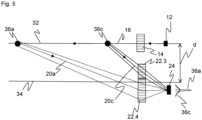
- figure 5 shows a schematic representation of the transmission and reception paths of a further embodiment of an optical sensor according to the invention, in which the optical meta-element 22 is divided into two partial elements 22 3 , 22 4 arranged next to one another in the direction of the light beam.
- both partial elements can have metamaterial and/or a metasurface on the front and/or rear.
- the first sub-element 22 3 acts on light bundles that have been remitted by objects in the near range
- the second sub-element 22 4 on light bundles that have been remitted by objects in the far range.
- the first sub-element 22 is 3 advantageously arranged closer to the transmission-side optical axis 32 than the second partial element 22 4 .
Landscapes
- Physics & Mathematics (AREA)
- Engineering & Computer Science (AREA)
- General Physics & Mathematics (AREA)
- Electromagnetism (AREA)
- Remote Sensing (AREA)
- Radar, Positioning & Navigation (AREA)
- Computer Networks & Wireless Communication (AREA)
- Optics & Photonics (AREA)
- Life Sciences & Earth Sciences (AREA)
- General Life Sciences & Earth Sciences (AREA)
- Geophysics (AREA)
- Measurement Of Optical Distance (AREA)
- Optical Radar Systems And Details Thereof (AREA)
Applications Claiming Priority (1)
| Application Number | Priority Date | Filing Date | Title |
|---|---|---|---|
| DE102021122418.7A DE102021122418B4 (de) | 2021-08-31 | 2021-08-31 | Optoelektronischer Sensor und Verfahren zum Erfassen von Objekten in einem Überwachungsbereich |
Publications (1)
| Publication Number | Publication Date |
|---|---|
| EP4141497A1 true EP4141497A1 (fr) | 2023-03-01 |
Family
ID=82851838
Family Applications (1)
| Application Number | Title | Priority Date | Filing Date |
|---|---|---|---|
| EP22189435.5A Withdrawn EP4141497A1 (fr) | 2021-08-31 | 2022-08-09 | Capteur optoélectronique et procédé de détection des objets dans une zone de surveillance |
Country Status (3)
| Country | Link |
|---|---|
| US (1) | US20230067699A1 (fr) |
| EP (1) | EP4141497A1 (fr) |
| DE (1) | DE102021122418B4 (fr) |
Cited By (1)
| Publication number | Priority date | Publication date | Assignee | Title |
|---|---|---|---|---|
| EP4517255A1 (fr) * | 2023-08-30 | 2025-03-05 | Sick Ag | Capture de données d'image 3d à l'aide d'un procédé de découpage de lumière |
Families Citing this family (2)
| Publication number | Priority date | Publication date | Assignee | Title |
|---|---|---|---|---|
| WO2025032201A1 (fr) * | 2023-08-10 | 2025-02-13 | Nil Technology Aps | Réduction d'impact de la lumière diffusée de zéro-ème ordre de diffraction ou autre lumière diffusée à faible angle d'un profil de transmission dans un système optique |
| CN122055661A (zh) * | 2023-09-20 | 2026-05-15 | 尼尔技术有限责任公司 | 减少不对称成像系统中的像差 |
Citations (5)
| Publication number | Priority date | Publication date | Assignee | Title |
|---|---|---|---|---|
| EP0735501B1 (fr) | 1995-03-27 | 2002-09-18 | Sick Ag | Arrangement de détecteurs de couleur pour lire des marquages en couleur |
| EP0924535B1 (fr) | 1997-12-18 | 2005-02-16 | Sick AG | Capteur opto-électronique |
| EP3018495B1 (fr) | 2014-11-07 | 2018-03-14 | Sick Ag | Capteur |
| EP3002609B1 (fr) | 2014-10-01 | 2018-08-15 | Sick Ag | Capteur optoelectronique |
| US20200284883A1 (en) * | 2019-03-08 | 2020-09-10 | Osram Gmbh | Component for a lidar sensor system, lidar sensor system, lidar sensor device, method for a lidar sensor system and method for a lidar sensor device |
Family Cites Families (1)
| Publication number | Priority date | Publication date | Assignee | Title |
|---|---|---|---|---|
| IL295272A (en) | 2020-02-10 | 2022-10-01 | Circle Optics Inc | Panoramic camera system for enhanced sensing |
-
2021
- 2021-08-31 DE DE102021122418.7A patent/DE102021122418B4/de active Active
-
2022
- 2022-08-09 EP EP22189435.5A patent/EP4141497A1/fr not_active Withdrawn
- 2022-08-30 US US17/823,228 patent/US20230067699A1/en active Pending
Patent Citations (5)
| Publication number | Priority date | Publication date | Assignee | Title |
|---|---|---|---|---|
| EP0735501B1 (fr) | 1995-03-27 | 2002-09-18 | Sick Ag | Arrangement de détecteurs de couleur pour lire des marquages en couleur |
| EP0924535B1 (fr) | 1997-12-18 | 2005-02-16 | Sick AG | Capteur opto-électronique |
| EP3002609B1 (fr) | 2014-10-01 | 2018-08-15 | Sick Ag | Capteur optoelectronique |
| EP3018495B1 (fr) | 2014-11-07 | 2018-03-14 | Sick Ag | Capteur |
| US20200284883A1 (en) * | 2019-03-08 | 2020-09-10 | Osram Gmbh | Component for a lidar sensor system, lidar sensor system, lidar sensor device, method for a lidar sensor system and method for a lidar sensor device |
Non-Patent Citations (2)
| Title |
|---|
| ORAD RESHEF ET AL: "An optic to replace space and its application towards ultra-thin imaging systems", ARXIV.ORG, CORNELL UNIVERSITY LIBRARY, 201 OLIN LIBRARY CORNELL UNIVERSITY ITHACA, NY 14853, 11 June 2021 (2021-06-11), XP081974600, DOI: 10.1038/S41467-021-23358-8 * |
| RESHEF, ORAD ET AL.: "An optic to replace space and its application towards ultra-thin imaging systems", NATURE COMMUNICATIONS, vol. 12, no. 1, 2021, pages 1 - 8 |
Cited By (1)
| Publication number | Priority date | Publication date | Assignee | Title |
|---|---|---|---|---|
| EP4517255A1 (fr) * | 2023-08-30 | 2025-03-05 | Sick Ag | Capture de données d'image 3d à l'aide d'un procédé de découpage de lumière |
Also Published As
| Publication number | Publication date |
|---|---|
| US20230067699A1 (en) | 2023-03-02 |
| DE102021122418A1 (de) | 2023-03-02 |
| DE102021122418B4 (de) | 2025-01-16 |
Similar Documents
| Publication | Publication Date | Title |
|---|---|---|
| EP2686700B1 (fr) | Dispositif de mesure de la distance séparant le dispositif de mesure et un objet cible à l'aide d'un rayonnement de mesure optique | |
| EP1405037B1 (fr) | Dispositif de mesure optique de distance sur une plage de mesure etendue | |
| DE102016213446B4 (de) | Optisches System zur Erfassung eines Abtastfelds | |
| DE102018118653B4 (de) | Optoelektronischer Sensor und Verfahren zum Erfassen eines Objekts | |
| DE102021122418B4 (de) | Optoelektronischer Sensor und Verfahren zum Erfassen von Objekten in einem Überwachungsbereich | |
| DE102015217908A1 (de) | Lidarsensor | |
| WO1999041568A9 (fr) | Systeme de mesure a scanner laser | |
| WO2007107413A1 (fr) | Dispositif de mesure optique de distances | |
| EP3432023B1 (fr) | Procédé de fabrication d'un capteur optoélectronique | |
| EP2210124B1 (fr) | Dispositif de mesure optique d'une distance | |
| EP3168642A1 (fr) | Capteur optoélectronique et procédé de détection d'un objet | |
| CH695633A5 (de) | Laserentfernungsmessgerät für den Nah- und Fernbereich mit speziellem Empfänger. | |
| DE102020109596B4 (de) | Optoelektronischer Sensor mit Blende und Herstellungsverfahren dafür | |
| EP4124884B1 (fr) | Capteur optoélectronique et procédé de détection d'un objet selon le principe de triangulation | |
| DE102021111949B4 (de) | Vorrichtung zur scannenden Messung des Abstands zu einem Objekt | |
| DE202021104670U1 (de) | Optoelektronischer Sensor zum Erfassen von Objekten in einem Überwachungsbereich | |
| DE102017129100B4 (de) | Optoelektronischer Sensor und Verfahren zur Erfassung eines Überwachungsbereichs | |
| WO2017005653A1 (fr) | Module détecteur pour un dispositif de détection optique | |
| EP0690317A1 (fr) | Méthode et dispositif pour la détermination optique des positions spatiales d'objets réfléchissants | |
| EP2479534A1 (fr) | Capteur optoelectrique | |
| DE19756541A1 (de) | Opto-elektronischer Sensor | |
| DE102015003392A1 (de) | Optische Triangulations-Sensoranordnung und Linsenanordnung hierfür | |
| WO2005108920A1 (fr) | Appareil d'acquisition de cible | |
| DE4343345A1 (de) | Verfahren und Vorrichtungen zur Messung der reflektiven bzw. transmittierenden optischen Eigenschaften einer Probe | |
| EP4517255B1 (fr) | Capture de données d'image 3d à l'aide d'un procédé de découpage de lumière |
Legal Events
| Date | Code | Title | Description |
|---|---|---|---|
| PUAI | Public reference made under article 153(3) epc to a published international application that has entered the european phase |
Free format text: ORIGINAL CODE: 0009012 |
|
| STAA | Information on the status of an ep patent application or granted ep patent |
Free format text: STATUS: THE APPLICATION HAS BEEN PUBLISHED |
|
| AK | Designated contracting states |
Kind code of ref document: A1 Designated state(s): AL AT BE BG CH CY CZ DE DK EE ES FI FR GB GR HR HU IE IS IT LI LT LU LV MC MK MT NL NO PL PT RO RS SE SI SK SM TR |
|
| STAA | Information on the status of an ep patent application or granted ep patent |
Free format text: STATUS: THE APPLICATION IS DEEMED TO BE WITHDRAWN |
|
| 18D | Application deemed to be withdrawn |
Effective date: 20230902 |