EP4141966A1 - Cellule solaire - Google Patents
Cellule solaire Download PDFInfo
- Publication number
- EP4141966A1 EP4141966A1 EP21867893.6A EP21867893A EP4141966A1 EP 4141966 A1 EP4141966 A1 EP 4141966A1 EP 21867893 A EP21867893 A EP 21867893A EP 4141966 A1 EP4141966 A1 EP 4141966A1
- Authority
- EP
- European Patent Office
- Prior art keywords
- solar cell
- layer
- metal
- heterojunction solar
- conductive layer
- Prior art date
- Legal status (The legal status is an assumption and is not a legal conclusion. Google has not performed a legal analysis and makes no representation as to the accuracy of the status listed.)
- Granted
Links
Images


Classifications
-
- H—ELECTRICITY
- H10—SEMICONDUCTOR DEVICES; ELECTRIC SOLID-STATE DEVICES NOT OTHERWISE PROVIDED FOR
- H10F—INORGANIC SEMICONDUCTOR DEVICES SENSITIVE TO INFRARED RADIATION, LIGHT, ELECTROMAGNETIC RADIATION OF SHORTER WAVELENGTH OR CORPUSCULAR RADIATION
- H10F10/00—Individual photovoltaic cells, e.g. solar cells
- H10F10/10—Individual photovoltaic cells, e.g. solar cells having potential barriers
- H10F10/16—Photovoltaic cells having only PN heterojunction potential barriers
- H10F10/164—Photovoltaic cells having only PN heterojunction potential barriers comprising heterojunctions with Group IV materials, e.g. ITO/Si or GaAs/SiGe photovoltaic cells
- H10F10/165—Photovoltaic cells having only PN heterojunction potential barriers comprising heterojunctions with Group IV materials, e.g. ITO/Si or GaAs/SiGe photovoltaic cells the heterojunctions being Group IV-IV heterojunctions, e.g. Si/Ge, SiGe/Si or Si/SiC photovoltaic cells
- H10F10/166—Photovoltaic cells having only PN heterojunction potential barriers comprising heterojunctions with Group IV materials, e.g. ITO/Si or GaAs/SiGe photovoltaic cells the heterojunctions being Group IV-IV heterojunctions, e.g. Si/Ge, SiGe/Si or Si/SiC photovoltaic cells the Group IV-IV heterojunctions being heterojunctions of crystalline and amorphous materials, e.g. silicon heterojunction [SHJ] photovoltaic cells
-
- H—ELECTRICITY
- H10—SEMICONDUCTOR DEVICES; ELECTRIC SOLID-STATE DEVICES NOT OTHERWISE PROVIDED FOR
- H10F—INORGANIC SEMICONDUCTOR DEVICES SENSITIVE TO INFRARED RADIATION, LIGHT, ELECTROMAGNETIC RADIATION OF SHORTER WAVELENGTH OR CORPUSCULAR RADIATION
- H10F71/00—Manufacture or treatment of devices covered by this subclass
- H10F71/138—Manufacture of transparent electrodes, e.g. transparent conductive oxides [TCO] or indium tin oxide [ITO] electrodes
-
- H—ELECTRICITY
- H10—SEMICONDUCTOR DEVICES; ELECTRIC SOLID-STATE DEVICES NOT OTHERWISE PROVIDED FOR
- H10F—INORGANIC SEMICONDUCTOR DEVICES SENSITIVE TO INFRARED RADIATION, LIGHT, ELECTROMAGNETIC RADIATION OF SHORTER WAVELENGTH OR CORPUSCULAR RADIATION
- H10F77/00—Constructional details of devices covered by this subclass
- H10F77/20—Electrodes
- H10F77/244—Electrodes made of transparent conductive layers, e.g. transparent conductive oxide [TCO] layers
-
- H—ELECTRICITY
- H10—SEMICONDUCTOR DEVICES; ELECTRIC SOLID-STATE DEVICES NOT OTHERWISE PROVIDED FOR
- H10F—INORGANIC SEMICONDUCTOR DEVICES SENSITIVE TO INFRARED RADIATION, LIGHT, ELECTROMAGNETIC RADIATION OF SHORTER WAVELENGTH OR CORPUSCULAR RADIATION
- H10F77/00—Constructional details of devices covered by this subclass
- H10F77/30—Coatings
- H10F77/306—Coatings for devices having potential barriers
- H10F77/311—Coatings for devices having potential barriers for photovoltaic cells
-
- H—ELECTRICITY
- H10—SEMICONDUCTOR DEVICES; ELECTRIC SOLID-STATE DEVICES NOT OTHERWISE PROVIDED FOR
- H10F—INORGANIC SEMICONDUCTOR DEVICES SENSITIVE TO INFRARED RADIATION, LIGHT, ELECTROMAGNETIC RADIATION OF SHORTER WAVELENGTH OR CORPUSCULAR RADIATION
- H10F77/00—Constructional details of devices covered by this subclass
- H10F77/30—Coatings
- H10F77/306—Coatings for devices having potential barriers
- H10F77/311—Coatings for devices having potential barriers for photovoltaic cells
- H10F77/315—Coatings for devices having potential barriers for photovoltaic cells the coatings being antireflective or having enhancing optical properties
-
- Y—GENERAL TAGGING OF NEW TECHNOLOGICAL DEVELOPMENTS; GENERAL TAGGING OF CROSS-SECTIONAL TECHNOLOGIES SPANNING OVER SEVERAL SECTIONS OF THE IPC; TECHNICAL SUBJECTS COVERED BY FORMER USPC CROSS-REFERENCE ART COLLECTIONS [XRACs] AND DIGESTS
- Y02—TECHNOLOGIES OR APPLICATIONS FOR MITIGATION OR ADAPTATION AGAINST CLIMATE CHANGE
- Y02E—REDUCTION OF GREENHOUSE GAS [GHG] EMISSIONS, RELATED TO ENERGY GENERATION, TRANSMISSION OR DISTRIBUTION
- Y02E10/00—Energy generation through renewable energy sources
- Y02E10/50—Photovoltaic [PV] energy
- Y02E10/548—Amorphous silicon PV cells
Definitions
- the present disclosure relates to the field of photovoltaics, and in particular to solar cells.
- Solar cells are designed to directly convert light energy into electricity. According to the photovoltaic effect, solar cells made of a single semiconductor material can only convert a part of the light energy in the solar radiation spectrum into electrical energy, which results in low energy conversion efficiency and low output voltage. Heterojunction solar cells are promising due to their bifacial power generation performance, but their photoelectric conversion efficiency still needs to be improved.
- the present disclosure provides a heterojunction solar cell.
- the heterojunction solar cell includes: an N-type wafer, where an i-type amorphous silicon oxide layer, a p-type amorphous silicon layer and a metal oxides-mixed conductive layer are sequentially arranged on a first surface of the N-type wafer; an i-type amorphous silicon oxide layer and an n-type amorphous silicon layer are sequentially arranged on a second surface of the N-type wafer; and the metal oxides-mixed conductive layer includes In 2 O 3 and an oxide of at least one subgroup metal.
- the subgroup metal may be one or more from the group consisting of Zn, Ce, Ti, Mo, Zr and W.
- the metal oxides-mixed conductive layer may include 80-100wt% of the In 2 O 3 , and the balance being the oxide of the subgroup metal and an inevitable impurity.
- the metal oxides-mixed conductive layer may include 0.1-10wt% of the oxide of the subgroup metal.
- the oxide of the subgroup metal may be ZnO, CeO 2 , TiO 2 , ZrO 2 , Mo 2 O 3 or WO 2 .
- the metal oxides-mixed conductive layer may have a thickness of 50-150 nm.
- the first surface defines a front side.
- the second surface defines a back side
- the metal oxides-mixed conductive layer may be provided on the n-type amorphous silicon layer.
- a composite conductive layer may be formed on the p-type amorphous silicon layer and/or the n-type amorphous silicon layer; the composite conductive layer may include an anti-reflection layer, a mixture coating and a transparent conductive layer; and the anti-reflection layer may be in electrical contact with the p-type amorphous silicon layer or the n-type amorphous silicon layer; and the mixture coating may be made of a metal mixed with a metal oxide, a metal mixed with a metal nitride, or a metal mixed with a metal oxide and a metal nitride.
- the metal in the mixture coating, may be one from the group consisting of Ag, Cu, Al, Mo, an Ag alloy, a Cu alloy, an Al alloy and a Mo alloy; and the metal oxide and the metal nitride may be respectively an oxide and a nitride formed by the metal; and the mixing coating may have a thickness of less than 10 nm.
- the Ag alloy may include greater than 50wt% of Ag, and the balance being one or more from the group consisting of Zn, Cu, In, Pt, Pd, Au, Nb, Nd, B, Bi and Ni;
- the Cu alloy may include greater than 50wt% of Cu, and the balance being one or more from the group consisting of Zn, Ag, In, Pt, Pd, Au, Nb, Nd, B, Bi and Ni;
- the Mo alloy may include greater than 80wt% of Mo, and the balance being one or more from the group consisting of Zn, Cu, In, Pt, Pd, Au, Nb, Nd, B, Bi and Ni;
- the Al alloy may include greater than 80wt% of Al, and the balance being one or more from the group consisting of Zn, Cu, In, Pt, Pd, Au, Nb, Nd, B, Bi and Ni.
- the transparent conductive layer may be made of one or more from the group consisting of In 2 O 3 , SnO 2 , ZnO, ITO, IZO, AZO, ITiO, ITiZO and FTO, and may have a thickness of 35-60 nm.
- the ITO may be doped with 0-50wt% of SnO 2 ; the IZO may be doped with 0-50wt% of ZnO; the AZO may be doped with 0-50wt% of Al 2 O 3 ; the ITiO may be doped with 0-10wt% of TiO 2 ; the ITiZO may be doped with 0-10wt% of TiO 2 and 0-40wt% of ZnO; and the FTO may be doped with 0-10wt% of F.
- a conductive weather-resistant layer may be further provided between the transparent conductive layer and the mixture coating.
- the weather-resistant layer may be made of one from the group consisting of TiN, ZnO, TiO 2 , SnO 2 , SiO 2 , Si 3 N 4 , AZO, IZO and YZO; and the weather-resistant layer may have a thickness of 2-200 nm.
- At least one sacrificial layer may be further provided between the anti-reflection layer and the mixture coating.
- the sacrificial layer may be made of one from the group consisting of Ti, Ni, Cr, NiCr, TiN, ZnO, TiO 2 , SnO 2 , SiO 2 , Nb 2 O 5 , Ta 2 O 5 and Si 3 N 4 ; and the sacrificial layer may have a thickness of 0.5-10 nm.
- the anti-reflection layer may be made of one from the group consisting of Nb 2 O 5 , Ta 2 O 5 , TiO 2 , SiN, ZnO and TiN, and may have a thickness of 25-45 nm.
- the present disclosure provides a metal oxides-mixed conductive layer in the solar cell, which significantly improves the mobility of carriers, reduces transmittance and resistance, and effectively improves photoelectric conversion efficiency.
- the present disclosure provides a composite conductive layer in the solar cell, which improves the transmittance of the heterojunction solar cell and further reduces the resistance, thereby improving the efficiency of the heterojunction solar cell.
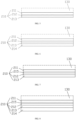
- FIG. 1 is a structural diagram of a heterojunction solar cell 1 according to a first embodiment of the present disclosure.
- the heterojunction solar cell 1 includes: an N-type wafer 100, where an i-type amorphous silicon oxide layer 110, a p-type amorphous silicon layer 120 and a metal oxides-mixed conductive layer 140 are sequentially arranged on a first surface of the N-type wafer; an i-type amorphous silicon oxide layer 110' and an n-type amorphous silicon layer 130 are sequentially arranged on a second surface of the N-type wafer; and the metal oxides-mixed conductive layer 140 includes In 2 O 3 and an oxide of at least one subgroup metal.
- the heterojunction solar cell 1 uses a metal oxides-mixed conductive layer 140 including In 2 O 3 and a subgroup metal oxide.
- ITO is often used as the conductive layer, and the mobility of carriers of the traditional ITO conductive layer is only 30-40 cm 2 /(V ⁇ s).
- the metal oxides-mixed conductive layer 140 of the present disclosure (equivalent to replacing at least part of Sn in ITO with a subgroup element) can significantly improve the mobility of carriers and effectively improve the photoelectric conversion efficiency.
- a silver gate line 150 is further formed on the mixed oxide conductive layer 140.
- a similar silver gate line 150 is further formed on the n-type amorphous silicon layer 130.
- the first surface defines a front side, that is, a side facing the sun, and the second surface defines a back side, that is, a side facing away from the sun.
- the metal oxides-mixed conductive layer 140 is provided on the n-type amorphous silicon layer 130 (i.e. on the side defined by the second surface). This helps to improve the photoelectric conversion efficiency of the heterojunction solar cell 1.
- Heterojunction solar cells with the above-mentioned metal oxides-mixed conductive layer were fabricated experimentally, and their related properties were tested.
- Embodiment 1 In and W oxides-mixed conductive layers are provided on both the p-type amorphous silicon layer 120 and the n-type amorphous silicon layer 130.
- Embodiment 2 In and Ce oxides-mixed conductive layers are provided on both the p-type amorphous silicon layer 120 and the n-type amorphous silicon layer 130.
- Embodiment 3 An In and Ti oxides-mixed conductive layer is provided on the p-type amorphous silicon layer 120 alone.
- Embodiment 4 An In and Zn oxides-mixed conductive layer is provided on the n-type amorphous silicon layer 130 alone.
- Embodiment 5 In and Mo oxides-mixed conductive layers are provided on both the p-type amorphous silicon layer 120 and the n-type amorphous silicon layer 130.
- Embodiment 6 An In and Zr oxides-mixed conductive layer is provided on the p-type amorphous silicon layer 120 alone.
- Embodiment 7 In, W and Sn oxides-mixed conductive layers are provided on both the p-type amorphous silicon layer 120 and the n-type amorphous silicon layer 130.
- ITO conductive layers commonly used in solar cells on the market are selected, and their related properties are shown in Table 1.
- Table 1 Material Mass ratio Thicknes s nm Transmittance % (300-1,100 nm) Resistanc e ohm Mobility cm 2 /(V ⁇ s ) Photoelectri c conversion efficiency
- Embodiment 1 IWO In 2 O 3 :WO 2 98:2 80 84 65 80 ⁇ 90 24.5%
- Embodiment 2 ICO In 2 O 3 :CeO 2 97.5:2. 5 80 83 70 140 ⁇ 150 25.3% Embodiment 3 ITiO ln 2 O 3 :TiO 2 99.7:0.
- a composite conductive layer 210 is provided on each (or on either) of the n-type amorphous silicon layer 130 and the p-type amorphous silicon layer 120.
- the composite conductive layer 210 includes an anti-reflection layer 211, a mixture coating 212 and a transparent conductive layer 213.
- the anti-reflection layer 211 is in electrical contact with the p-type amorphous silicon layer 120 or the n-type amorphous silicon layer 130.
- the mixture coating 212 is made of a metal mixed with a metal oxide, a metal mixed with a metal nitride, or a metal mixed with a metal oxide and a metal nitride.
- the anti-reflection layer 211 is in electrical contact with the n-type amorphous silicon layer 130, and a silver gate line 216 is further formed on the transparent conductive layer 213 to connect an external circuit.
- the composite conductive layer 210 is formed on the n-type amorphous silicon layer 130 and/or the p-type amorphous silicon layer 120. This increases the transmittance of the heterojunction solar cell 1 and further reduces the resistance thereof, thereby increasing the efficiency of the heterojunction solar cell 1.
- the metal oxides-mixed conductive layer 140 as described above is further formed on the composite conductive layer 210. That is, the transparent conductive layer 213 is in contact with the metal oxides-mixed conductive layer 140. A silver gate line 216 is formed on the metal oxides-mixed conductive layer 140. With this structure, the heterojunction solar cell 1 has high transmittance and low resistance, thereby achieving high photoelectric conversion efficiency.
- the anti-reflection layer 211 is made of one from the group consisting of Nb 2 O 5 , Ta 2 O 5 , TiO 2 , SiN, ZnO and TiN, and has a thickness of 25-45 nm.
- the anti-reflection layer 211 is used to improve the sunlight injection efficiency of the back side of the heterojunction solar cell 1, thereby improving the efficiency of the heterojunction solar cell 1.
- the transparent conductive layer 213 is made of a metal oxide, and has a thickness of 35-60 nm.
- the metal oxide is one or more from the group consisting of In 2 O 3 , SnO 2 , ZnO, ITO, IZO, AZO, ITiO, ITiZO and FTO.
- the ITO is doped with 0-50wt% of SnO 2 ; the IZO is doped with 0-50wt% of ZnO; the AZO is doped with 0-50wt% of Al 2 O 3 ; the ITiO is doped with 0-10wt% of TiO 2 ; the ITiZO is doped with 0-10wt% of TiO 2 and 0-40wt% of ZnO; and the FTO is doped with 0-10wt% of F.
- a mixture coating 212 with a thickness of less than 10 nm is added on the basis of the transparent conductive layer 213 to further reduce the resistance of the composite conductive layer 210.
- the mixture coating 212 is fabricated by a physical vapor deposition (PVD) process.
- PVD physical vapor deposition
- a small amount of oxygen and/or nitrogen is introduced into a reaction chamber.
- the target includes Ag, Cu, Al, Mo, an Ag alloy, a Cu alloy, an Al alloy or a Mo alloy.
- the Ag alloy includes greater than 50wt% of Ag, and the balance being one or more from the group consisting of Zn, Cu, In, Pt, Pd, Au, Nb, Nd, B, Bi and Ni.
- the Cu alloy includes greater than 50wt% of Cu, and the balance being one or more from the group consisting of Zn, Ag, In, Pt, Pd, Au, Nb, Nd, B, Bi and Ni.
- the Mo alloy includes greater than 80wt% of Mo, and the balance being one or more from the group consisting of Zn, Cu, In, Pt, Pd, Au, Nb, Nd, B, Bi and Ni.
- the Al alloy includes greater than 80wt% of Al, and the balance being one or more from the group consisting of Zn, Cu, In, Pt, Pd, Au, Nb, Nd, B, Bi and Ni.
- the mixture coating 212 and the transparent conductive layer 213 are provided on the anti-reflection layer 211. This lowers the resistance and further improves the solar injection efficiency of the back side of the heterojunction solar cell 1, thereby further improving the efficiency of the heterojunction solar cell 1.
- a conductive weather-resistant layer 214 is further provided between the transparent conductive layer 212 and the mixture coating 213.
- the weather-resistant layer 214 has a thickness of 2-200 nm, and is made of one from the group consisting of TiN, ZnO, TiO 2 , SnO 2 , SiO 2 , Si 3 N 4 , AZO, IZO and YZO.
- the weather-resistant layer 214 can prevent the mixture coating 212 from being eroded by water vapor, oxygen, etc. in the environment, ensure the performance stability of the composite conductive layer 210, and prolong the service life.
- a sacrificial layer 215 with a thickness of 0.5-10 nm is further provided between the anti-reflection layer 211 and the mixture coating 212.
- the sacrificial layer is made of one from the group consisting of Ti, Ni, Cr, NiCr, TiN, ZnO, TiO 2 , SnO 2 , SiO 2 , Nb 2 O 5 , Ta 2 O 5 and Si 3 N 4 .
- the sacrificial layer 215 is provided between the mixture coating 143 and the n-type amorphous silicon layer 130.
- Heterojunction solar cells with a composite conductive layer 210 on the back side were also fabricated, and the composition of the composite conductive layer is shown in Table 2.
- the composite conductive layer is located on the back side of the heterojunction solar cell.
- the composite conductive layer is located on the front side of the heterojunction solar cell.
- the composite conductive layer is located on both sides of the heterojunction solar cell.
- ITO is used.
- the performance test results of Embodiments 11 to 17 and Comparative Embodiment 10 are shown in Table 3.
Landscapes
- Photovoltaic Devices (AREA)
Applications Claiming Priority (3)
| Application Number | Priority Date | Filing Date | Title |
|---|---|---|---|
| CN202110754052.8A CN113488556A (zh) | 2021-07-04 | 2021-07-04 | 混合金属氧化物导电薄膜及异质结太阳能电池 |
| CN202110754051.3A CN113488548A (zh) | 2021-07-04 | 2021-07-04 | 复合导电膜及异质结太阳能电池 |
| PCT/CN2021/127785 WO2023279598A1 (fr) | 2021-07-04 | 2021-10-30 | Cellule solaire |
Publications (4)
| Publication Number | Publication Date |
|---|---|
| EP4141966A1 true EP4141966A1 (fr) | 2023-03-01 |
| EP4141966A4 EP4141966A4 (fr) | 2023-03-01 |
| EP4141966C0 EP4141966C0 (fr) | 2026-02-18 |
| EP4141966B1 EP4141966B1 (fr) | 2026-02-18 |
Family
ID=82020829
Family Applications (1)
| Application Number | Title | Priority Date | Filing Date |
|---|---|---|---|
| EP21867893.6A Active EP4141966B1 (fr) | 2021-07-04 | 2021-10-30 | Cellule solaire |
Country Status (2)
| Country | Link |
|---|---|
| EP (1) | EP4141966B1 (fr) |
| WO (1) | WO2023279598A1 (fr) |
Citations (5)
| Publication number | Priority date | Publication date | Assignee | Title |
|---|---|---|---|---|
| JP2013161822A (ja) * | 2012-02-01 | 2013-08-19 | Mitsubishi Electric Corp | 太陽電池およびその製造方法、太陽電池モジュール |
| CN106340570A (zh) * | 2016-10-27 | 2017-01-18 | 中国科学院上海微系统与信息技术研究所 | 一种用于制作透明导电氧化物薄膜的镀膜设备及镀膜方法 |
| CN108987488A (zh) * | 2017-05-31 | 2018-12-11 | 国家电投集团科学技术研究院有限公司 | 硅异质结太阳电池及其制备方法 |
| CN113488548A (zh) * | 2021-07-04 | 2021-10-08 | 北京载诚科技有限公司 | 复合导电膜及异质结太阳能电池 |
| CN113488556A (zh) * | 2021-07-04 | 2021-10-08 | 北京载诚科技有限公司 | 混合金属氧化物导电薄膜及异质结太阳能电池 |
Family Cites Families (6)
| Publication number | Priority date | Publication date | Assignee | Title |
|---|---|---|---|---|
| CN106601861A (zh) * | 2015-10-14 | 2017-04-26 | 福建金石能源有限公司 | 一种异质结太阳能电池的退火方法 |
| KR102704085B1 (ko) * | 2017-01-20 | 2024-09-06 | 트리나 솔라 컴패니 리미티드 | 이종 접합 태양전지 및 이의 제조 방법 |
| CN110649129A (zh) * | 2019-09-19 | 2020-01-03 | 国家电投集团科学技术研究院有限公司 | 硅异质结太阳电池 |
| CN111446028A (zh) * | 2020-04-28 | 2020-07-24 | 北京载诚科技有限公司 | 一种透明导电膜与触控屏 |
| CN111710759B (zh) * | 2020-06-19 | 2022-11-11 | 中威新能源(成都)有限公司 | 一种shj太阳电池tco薄膜表面处理方法 |
| CN212848452U (zh) * | 2020-08-21 | 2021-03-30 | 嘉兴阿特斯光伏技术有限公司 | 异质结太阳能电池 |
-
2021
- 2021-10-30 WO PCT/CN2021/127785 patent/WO2023279598A1/fr not_active Ceased
- 2021-10-30 EP EP21867893.6A patent/EP4141966B1/fr active Active
Patent Citations (5)
| Publication number | Priority date | Publication date | Assignee | Title |
|---|---|---|---|---|
| JP2013161822A (ja) * | 2012-02-01 | 2013-08-19 | Mitsubishi Electric Corp | 太陽電池およびその製造方法、太陽電池モジュール |
| CN106340570A (zh) * | 2016-10-27 | 2017-01-18 | 中国科学院上海微系统与信息技术研究所 | 一种用于制作透明导电氧化物薄膜的镀膜设备及镀膜方法 |
| CN108987488A (zh) * | 2017-05-31 | 2018-12-11 | 国家电投集团科学技术研究院有限公司 | 硅异质结太阳电池及其制备方法 |
| CN113488548A (zh) * | 2021-07-04 | 2021-10-08 | 北京载诚科技有限公司 | 复合导电膜及异质结太阳能电池 |
| CN113488556A (zh) * | 2021-07-04 | 2021-10-08 | 北京载诚科技有限公司 | 混合金属氧化物导电薄膜及异质结太阳能电池 |
Non-Patent Citations (3)
| Title |
|---|
| KOBAYASHI EIJI ET AL: "Cerium oxide and hydrogen co-doped indium oxide films for high-efficiency silicon heterojunction solar cells", SOLAR ENERGY MATERIALS AND SOLAR CELLS, ELSEVIER SCIENCE PUBLISHERS, AMSTERDAM, NL, vol. 149, 22 January 2016 (2016-01-22), pages 75 - 80, XP029454584, ISSN: 0927-0248, DOI: 10.1016/J.SOLMAT.2016.01.005 * |
| LEONARD TUTSCH ET AL: "The sputter deposition of broadband transparent and highly conductive cerium and hydrogen co-doped indium oxide and its transfer to silicon heterojunction solar cells", PROGRESS IN PHOTOVOLTAICS: RESEARCH AND APPLICATIONS, JOHN WILEY & SONS, LTD, HOBOKEN, USA, vol. 29, no. 7, 5 February 2021 (2021-02-05), pages 835 - 845, XP071979562, ISSN: 1062-7995, DOI: 10.1002/PIP.3388 * |
| See also references of WO2023279598A1 * |
Also Published As
| Publication number | Publication date |
|---|---|
| WO2023279598A1 (fr) | 2023-01-12 |
| EP4141966C0 (fr) | 2026-02-18 |
| EP4141966B1 (fr) | 2026-02-18 |
Similar Documents
| Publication | Publication Date | Title |
|---|---|---|
| EP2092571B1 (fr) | Électrode avant à couche pelliculaire métallique mince et couche tampon hautement fonctionnelle utilisée dans un dispositif photovoltaïque et son procédé de réalisation | |
| RU2413333C2 (ru) | Передний контакт на основе оксида индия-цинка для фотоэлектрического прибора и способ его изготовления | |
| US4272641A (en) | Tandem junction amorphous silicon solar cells | |
| US20090194165A1 (en) | Ultra-high current density cadmium telluride photovoltaic modules | |
| US20080223430A1 (en) | Buffer layer for front electrode structure in photovoltaic device or the like | |
| US8519435B2 (en) | Flexible photovoltaic cells having a polyimide material layer and method of producing same | |
| US12125932B2 (en) | Stacked solar cell | |
| EP2976783A1 (fr) | Dispositif photovoltaïque comprenant un contact arrière et procédé de fabrication | |
| US20100218820A1 (en) | Solar cell and method of fabricating the same | |
| CN103956391B (zh) | 一种AZO/Si异质结太阳电池及其制备方法 | |
| KR102241098B1 (ko) | 수소화된 p-i-n층을 포함하는 반투명 비정질 실리콘 박막 태양전지 및 이의 제조방법 | |
| WO2022071302A1 (fr) | Procédé de production de cellule solaire à film mince de pérovskite | |
| US20120103407A1 (en) | Solar cell and method for manufacturing the solar cell | |
| EP4141966A1 (fr) | Cellule solaire | |
| JP2002217429A (ja) | 光電変換素子 | |
| CN113488548A (zh) | 复合导电膜及异质结太阳能电池 | |
| GB2047463A (en) | Amorphous silicon solar cells | |
| CN111900228B (zh) | 一种面向晶硅太阳电池的电子选择性接触 | |
| US12125931B2 (en) | Tandem solar cell | |
| KR20140140187A (ko) | 산화아연계 스퍼터링 타겟 및 이를 통해 증착된 보호층을 갖는 광전지 | |
| KR102849564B1 (ko) | 양면수광형 박막태양전지 및 그 제조방법 | |
| CN210403774U (zh) | 一种背接触无掺杂异质结-钙钛矿叠层太阳电池 | |
| KR101571652B1 (ko) | 산화아연계 스퍼터링 타겟 및 이를 통해 증착된 보호층을 갖는 광전지 | |
| CN116137296A (zh) | 大幅提升p型晶体硅电池效率的非pn结面工艺结构 | |
| JP4352111B2 (ja) | 光電変換装置およびその製造方法 |
Legal Events
| Date | Code | Title | Description |
|---|---|---|---|
| STAA | Information on the status of an ep patent application or granted ep patent |
Free format text: STATUS: UNKNOWN |
|
| STAA | Information on the status of an ep patent application or granted ep patent |
Free format text: STATUS: THE INTERNATIONAL PUBLICATION HAS BEEN MADE |
|
| PUAI | Public reference made under article 153(3) epc to a published international application that has entered the european phase |
Free format text: ORIGINAL CODE: 0009012 |
|
| STAA | Information on the status of an ep patent application or granted ep patent |
Free format text: STATUS: REQUEST FOR EXAMINATION WAS MADE |
|
| 17P | Request for examination filed |
Effective date: 20220323 |
|
| A4 | Supplementary search report drawn up and despatched |
Effective date: 20221117 |
|
| AK | Designated contracting states |
Kind code of ref document: A1 Designated state(s): AL AT BE BG CH CY CZ DE DK EE ES FI FR GB GR HR HU IE IS IT LI LT LU LV MC MK MT NL NO PL PT RO RS SE SI SK SM TR |
|
| STAA | Information on the status of an ep patent application or granted ep patent |
Free format text: STATUS: EXAMINATION IS IN PROGRESS |
|
| 17Q | First examination report despatched |
Effective date: 20230911 |
|
| DAV | Request for validation of the european patent (deleted) | ||
| DAX | Request for extension of the european patent (deleted) | ||
| REG | Reference to a national code |
Ref country code: DE Ref legal event code: R079 Free format text: PREVIOUS MAIN CLASS: H01L0031021600 Ref country code: DE Ref legal event code: R079 Ref document number: 602021048410 Country of ref document: DE Free format text: PREVIOUS MAIN CLASS: H01L0031021600 Ipc: H10F0010166000 |
|
| GRAP | Despatch of communication of intention to grant a patent |
Free format text: ORIGINAL CODE: EPIDOSNIGR1 |
|
| STAA | Information on the status of an ep patent application or granted ep patent |
Free format text: STATUS: GRANT OF PATENT IS INTENDED |
|
| RIC1 | Information provided on ipc code assigned before grant |
Ipc: H10F 10/166 20250101AFI20251021BHEP Ipc: H10F 77/20 20250101ALI20251021BHEP Ipc: H10F 77/30 20250101ALI20251021BHEP Ipc: H10F 71/00 20250101ALI20251021BHEP |
|
| INTG | Intention to grant announced |
Effective date: 20251111 |
|
| GRAS | Grant fee paid |
Free format text: ORIGINAL CODE: EPIDOSNIGR3 |
|
| GRAA | (expected) grant |
Free format text: ORIGINAL CODE: 0009210 |
|
| STAA | Information on the status of an ep patent application or granted ep patent |
Free format text: STATUS: THE PATENT HAS BEEN GRANTED |
|
| AK | Designated contracting states |
Kind code of ref document: B1 Designated state(s): AL AT BE BG CH CY CZ DE DK EE ES FI FR GB GR HR HU IE IS IT LI LT LU LV MC MK MT NL NO PL PT RO RS SE SI SK SM TR |
|
| REG | Reference to a national code |
Ref country code: CH Ref legal event code: F10 Free format text: ST27 STATUS EVENT CODE: U-0-0-F10-F00 (AS PROVIDED BY THE NATIONAL OFFICE) Effective date: 20260218 Ref country code: GB Ref legal event code: FG4D |
|
| REG | Reference to a national code |
Ref country code: IE Ref legal event code: FG4D |
|
| REG | Reference to a national code |
Ref country code: DE Ref legal event code: R096 Ref document number: 602021048410 Country of ref document: DE |
|
| U01 | Request for unitary effect filed |
Effective date: 20260303 |
|
| U07 | Unitary effect registered |
Designated state(s): AT BE BG DE DK EE FI FR IT LT LU LV MT NL PT RO SE SI Effective date: 20260310 |