EP4145355B1 - Dispositif de calcul - Google Patents
Dispositif de calcul Download PDFInfo
- Publication number
- EP4145355B1 EP4145355B1 EP22157123.5A EP22157123A EP4145355B1 EP 4145355 B1 EP4145355 B1 EP 4145355B1 EP 22157123 A EP22157123 A EP 22157123A EP 4145355 B1 EP4145355 B1 EP 4145355B1
- Authority
- EP
- European Patent Office
- Prior art keywords
- variables
- calculation
- circuit
- time
- cores
- Prior art date
- Legal status (The legal status is an assumption and is not a legal conclusion. Google has not performed a legal analysis and makes no representation as to the accuracy of the status listed.)
- Active
Links
Images


Classifications
-
- G—PHYSICS
- G06—COMPUTING OR CALCULATING; COUNTING
- G06N—COMPUTING ARRANGEMENTS BASED ON SPECIFIC COMPUTATIONAL MODELS
- G06N5/00—Computing arrangements using knowledge-based models
- G06N5/01—Dynamic search techniques; Heuristics; Dynamic trees; Branch-and-bound
-
- G—PHYSICS
- G06—COMPUTING OR CALCULATING; COUNTING
- G06F—ELECTRIC DIGITAL DATA PROCESSING
- G06F17/00—Digital computing or data processing equipment or methods, specially adapted for specific functions
- G06F17/10—Complex mathematical operations
- G06F17/11—Complex mathematical operations for solving equations, e.g. nonlinear equations, general mathematical optimization problems
-
- G—PHYSICS
- G06—COMPUTING OR CALCULATING; COUNTING
- G06F—ELECTRIC DIGITAL DATA PROCESSING
- G06F17/00—Digital computing or data processing equipment or methods, specially adapted for specific functions
- G06F17/10—Complex mathematical operations
- G06F17/16—Matrix or vector computation, e.g. matrix-matrix or matrix-vector multiplication, matrix factorization
-
- G—PHYSICS
- G06—COMPUTING OR CALCULATING; COUNTING
- G06F—ELECTRIC DIGITAL DATA PROCESSING
- G06F9/00—Arrangements for program control, e.g. control units
- G06F9/06—Arrangements for program control, e.g. control units using stored programs, i.e. using an internal store of processing equipment to receive or retain programs
- G06F9/46—Multiprogramming arrangements
- G06F9/50—Allocation of resources, e.g. of the central processing unit [CPU]
- G06F9/5005—Allocation of resources, e.g. of the central processing unit [CPU] to service a request
- G06F9/5027—Allocation of resources, e.g. of the central processing unit [CPU] to service a request the resource being a machine, e.g. CPUs, Servers, Terminals
-
- G—PHYSICS
- G06—COMPUTING OR CALCULATING; COUNTING
- G06N—COMPUTING ARRANGEMENTS BASED ON SPECIFIC COMPUTATIONAL MODELS
- G06N7/00—Computing arrangements based on specific mathematical models
- G06N7/01—Probabilistic graphical models, e.g. probabilistic networks
-
- G—PHYSICS
- G06—COMPUTING OR CALCULATING; COUNTING
- G06N—COMPUTING ARRANGEMENTS BASED ON SPECIFIC COMPUTATIONAL MODELS
- G06N7/00—Computing arrangements based on specific mathematical models
- G06N7/08—Computing arrangements based on specific mathematical models using chaos models or non-linear system models
Definitions
- the present disclosure relates to a calculation device.
- Combinatorial optimization is the problem of finding a combination of discrete values that minimizes a discrete-variable function called a cost function.
- the Ising problem is a combinatorial optimization problem of minimizing the Ising energy.
- the Ising energy is a cost function given by a quadratic function of Ising spins that are binary variables. The Ising machine can solve such Ising problems fast.
- the Ising machine is implemented by hardware, for example, by a quantum annealer, a coherent Ising machine, and a quantum bifurcation machine.
- the quantum annealer implements quantum annealing using superconducting circuitry.
- the coherent Ising machine uses the oscillation phenomenon of a network formed with optical parametric oscillators.
- the quantum bifurcation machine uses a quantum-mechanical bifurcation phenomenon in a network of parametric oscillators having Kerr effect. While the Ising machine implemented by such hardware may achieve significant reduction of computation time, scale increase and stable operation are difficult.
- a solution to the Ising problem can be calculated using computational resources such as widespread digital computers or operation circuits.
- Digital computers can be increased in scale and stably operated, compared with quantum annealers, coherent Ising machines, and quantum bifurcation machines.
- the Ising machines using computational resources are limited in calculation scale and calculation speed by the computational resources.
- computational resources In order to improve the calculation scale and the calculation speed of such Ising machines, computational resources have to be increased. Increasing the computational resources, however, is not easy due to many technical difficulties in, for example, semiconductor manufacturing processes.
- Ising machines configured with a large number of computational resources using scale-out technology may be improved in performance depending on the number of computational resources.
- the Ising machine configured with a large number of computational resources need to exchange information between the computational resources to perform calculations, the total calculation time is prolonged due to the communication overhead between the computational resources.
- the problem to be solved by the present disclosure is to solve large-scale optimization problems fast while preventing the total computation time from being prolonged due to communication overhead.
- US 2021/182356 relates to an information processing device that includes a first processing circuit and a second processing circuit.
- the first processing circuit is configured to update a third vector based on basic equations. Each of the basic equations is a partial derivative of an objective function with respect to either of the variables in the objective function.
- the second processing circuit is configured to update the element of the first vector and update the element of the second vector. The element of the first vector smaller than a first value is set to the first value. The element of the first vector greater than a second value is set to the second value.
- the present invention provides a calculation device as recited in claim 1.
- s i and s j are spins.
- the spin is a binary variable that takes a value of either +1 or -1.
- s i is the ith spin of N spins.
- s j is the jth spin of N spins.
- i and j are an integer of 1 through N, both inclusive.
- N denotes the number of spins and is an integer equal to or greater than 2.
- h is an array of bias coefficient representing a force acting on each individual spin.
- h i is the bias coefficient representing a force acting on the ith spin.
- J is a matrix of coupling coefficient representing a force acting between two spins.
- J is an N ⁇ N real symmetric matrix in which diagonal components are zero.
- J i,j denotes a coefficient of an element at the ith row and jth column of J. In other words, J i,j is the coupling coefficient representing a force acting between the ith spin and the jth spin.
- the Ising machine sets the energy E written by Equation (1) as an objective function and calculates a solution that makes the energy E as small as possible.
- the solution of the Ising model (s 1 , s 2 , ..., s N ) in which the energy E has the minimum value is called optimal solution.
- the solution of the Ising model is not necessarily an optimal solution but may be an approximate solution in which the energy E is close to the minimum value.
- the Ising problem may be a problem to calculate not only an optimal solution but also an approximate solution.
- a 0-1 combinatorial optimization problem with an objective function which is a quadratic function with a discrete variable (bit) taking either 0 or 1 is called a 0-1 quadratic programming problem.
- the discrete variable (bit) is converted into s i by using a computation of (1 + s i )/2. That is, it can be said that the 0-1 quadratic programming problem is equivalent to the Ising problem given by Equation (1). Therefore, the 0-1 quadratic programming problem can be converted into the Ising problem to be solved by the Ising machine.
- Hayato Goto Kosuke Tatsumura, Alexander R. Dixon, "Combinatorial optimization by simulating adiabatic bifurcations in nonlinear Hamiltonian systems", Science Advances, Vol. 5, no. 4, eaav2372, 19 Apr. 2019 ; and H. Goto, K. Endo, M. Suzuki, Y. Sakai, T. Kanao, Y. Hamakawa, R. Hidaka, M. Yamasaki, K. Tatsumura, "High-performance combinatorial optimization based on classical mechanics", Science Advances; 7, eabe7953", Feb. 2021 propose a simulated bifurcation algorithm as an algorithm for solving a 0-1 combinatorial optimization problem.
- the simulated bifurcation algorithm can solve a large-scale 0-1 combinatorial optimization problem fast using an Ising model implemented by a digital computer.
- the simulated bifurcation algorithm also can solve a large-scale 0-1 combinatorial optimization problem fast with electronic circuitry such as a central processing unit (CPU), a microprocessor, a graphics processing unit (GPU), a field-programmable gate array (FPGA), an application specific integrated circuit (ASIC), or a combination circuit thereof.
- CPU central processing unit
- microprocessor a graphics processing unit
- GPU graphics processing unit
- FPGA field-programmable gate array
- ASIC application specific integrated circuit
- the simulated bifurcation algorithm uses N first variables x i and N second variables y i corresponding to virtual N oscillators.
- each of N oscillators represents a virtual particle having one degree of freedom. In other words, each of N oscillators virtually changes its position and momentum in one dimensional direction.
- N oscillators correspond one-to-one with N spins in the Ising problem. Therefore, N oscillators correspond one-to-one with N discrete variables of a combinatorial optimization problem.
- Both the first variable x i and the second variable y i are continuous variables represented by real numbers.
- the ith first variable x i denotes the position of the ith oscillator among N oscillators.
- the ith second variable y i denotes the momentum of the ith oscillator.
- i denotes an integer of 1 through N, both inclusive, and denotes an index that identifies each of N oscillators.
- Equation (2) The basic simulated bifurcation algorithm numerically solves simultaneous ordinary differential equations in Equation (2) below for N first variables x i and N second variables y i .
- H is the Hamiltonian in Equation (3) below.
- the coefficient D is a predetermined constant and corresponds to detuning.
- the coefficient p(t) corresponds to pumping amplitude and its value monotonously increases according to the number of times of updating in calculation of the simulated bifurcation algorithm.
- the variable t represents time.
- the initial value of the coefficient p(t) may be set to 0.
- K is a predetermined constant and corresponds to a positive Kerr coefficient. K may be zero.
- f i is an external force and given by Equation (4) below.
- Equation (4) b i is given by a partial derivative of the expression inside the parentheses in Equation (3) with respect to the first variable x i .
- the expression inside the parentheses in Equation (3) corresponds to the energy E of the Ising model.
- c is a coefficient. c may be, for example, a constant determined in advance before calculation is performed. Furthermore, ⁇ (t) is a coefficient increasing with p(t).
- the simulated bifurcation algorithm calculates the value of the spin s i , based on the sign of the first variable x i after the value of p(t) is increased from an initial value (for example, 0) to a prescribed value.
- the simulated bifurcation algorithm solves differential equations given by Equation (2), Equation (3), and Equation (4) using the symplectic Euler method.
- Equation (2) the differential equations given by Equation (2), Equation (3), and Equation (4) can be written into a discrete recurrence relation given by Equation (5).
- t is time.
- ⁇ t is a time step (unit time, time step size).
- a digital computer or an electronic circuit such as an FPGA updates N first variables x i and N second variables y i sequentially for each time step from the initial time and alternately between the first variables x i and the second variables y i , based on the algorithm in Equation (5).
- the digital computer or the electronic circuit such as an FPGA then binarizes the values of N first variables x i at the end time using the signum function and outputs the values of N spins.
- Equation (5) is written using time t and time step ⁇ t in order to show the correspondence with the differential equations.
- the algorithm for computing Equation (5) may not necessarily include time t or time step ⁇ t as explicit parameters.
- time step ⁇ t is 1, the algorithm for computing Equation (5) need not include time step ⁇ t.
- time t is not included as an explicit parameter, the algorithm for computing Equation (5) performs a process with x i (t+ ⁇ t) as the updated value of x i (t).
- the algorithm for computing Equation (5) performs a process using "t" as a parameter that identifies a variable at a time step before update and "t+ ⁇ t" as a parameter that identifies a variable at a time step after update.
- FIG. 1 is a diagram illustrating a bifurcation phenomenon of the first variables x i obtained when an optimization problem is solved by the basic simulated bifurcation algorithm.
- a bifurcation phenomenon occurs, that is, a system with a single stable motion state changes to a system with two stable motion states as the parameters in the system change.
- the first variables x i are concentrated on the vicinity of -1 or +1.
- the change in position and momentum of a plurality of oscillators by the passage of time is called time evolution.
- the simulation of such time evolution with computational resources is called time evolution simulation.
- a dynamical system in which N oscillators interact with each other is called an N-body oscillator system.
- the simulated bifurcation algorithm achieves the search for ground states of the Ising spin model corresponding to the combinatorial optimization problem by the time evolution simulation of the N-body oscillator system.
- the simulated bifurcation algorithm updates N first variables x i and N second variables y i sequentially for each time step from the initial time to the end time and alternately between the first variables x i and the second variables y i . In this way, the simulated bifurcation algorithm can perform the time evolution simulation of the N-body oscillator system.
- the simulated bifurcation algorithm performs an interaction operation to calculate the interaction between oscillators and a time evolution operation to calculate the time evolution of oscillators.
- the simulated bifurcation algorithm performs the interaction operation and the time evolution operation at each time step from the initial time to the end time.
- the interaction operation is an operation to calculate N b i in Equation (4).
- b i is called an intermediate variable.
- the input values necessary for calculating the ith intermediate variable b i are N first variables x i calculated at the previous time step.
- the time evolution operation is an operation to calculate x i (t+ ⁇ t) and y i (t+ ⁇ t) in Equation (5).
- the input values necessary for calculating the ith first variable x i (t+ ⁇ t) and the ith second variable y i (t+ ⁇ t) are the ith intermediate variable b i calculated by the time evolution operation, the ith x i (t) calculated at the previous time step, and the ith y i (t) calculated at the previous time step.
- the simulated bifurcation algorithm may perform a portion of the time evolution operation before the interaction operation.
- each of N first variables x i may be multiplied in advance by a coefficient multiplied by the time evolution operation, prior to the interaction operation.
- the simulated bifurcation algorithm may perform the interaction operation after multiplying each of N first variables x i by constants -c and ⁇ t in advance.
- the variable x i multiplied by -c ⁇ t may be denoted as x' i . Since x' i is a variable obtained by multiplying x i by a coefficient, x' i is not different from x i in that it is a variable representing the position of the corresponding oscillator.
- the 0-1 combinatorial optimization problem can be solved fast not only using the basic simulated bifurcation algorithm as described above but also using an improved simulated bifurcation algorithm of the basic simulated bifurcation algorithm.
- the simulated bifurcation algorithm may be an algorithm in which the updating order of the first variables x i and the second variables y i at each time step is interchanged.
- the simulated bifurcation algorithm may perform a momentum update process and a position update process alternately a predetermined number of times in the time evolution operation for a single time step.
- the momentum update process is a process of calculating the difference of momentum ⁇ y i after a minute time shorter than the time step by the FX function using the first variable x i representing the position as an input, and updating the second variable y i with the calculated difference of momentum ⁇ y i .
- the position update process is a process of calculating the difference of position ⁇ x i after a minute time by the FY function using the second variable y i representing the momentum as an input, and updating the first variable x i with the calculated difference of position ⁇ x i .
- the simulated bifurcation algorithm may also perform the computation by setting K in Equation (5) to 0 and limiting the range of both or one of the first variable x i and the second variable y i to within a predetermined range (for example, -1 through +1, both inclusive).
- the simulated bifurcation algorithm may also binarize the value of the first variable x i by the signum function sgn(x i ) in the computation at each time step.
- the simulated bifurcation algorithm may also perform a predetermined manipulation (for example, manipulations such as adding a predetermined value, multiplying a predetermined value, adding a random number, or multiplying a random number) on one or both of the first variable x i and the second variable y i under a predetermined condition, in the computation at each time step.
- a predetermined manipulation for example, manipulations such as adding a predetermined value, multiplying a predetermined value, adding a random number, or multiplying a random number
- the simulated bifurcation algorithm may be any algorithm that adds the effect of the bifurcation phenomenon to the first variables x i with time evolution and updates N first variables x i and N second variables y i sequentially for each time step from the initial time to the end time and alternately between the first variables x i and the second variables y i .
- FIG. 2 is a diagram illustrating a configuration of a calculation device 10 according to the present arrangement.
- the calculation device 10 outputs the solution of the optimization problem with N discrete variables, using the simulated bifurcation algorithm.
- the calculation device 10 includes a network 12, P calculation cores 14, and a management device 16.
- P is an integer equal to or greater than 2.
- the calculation device 10 includes a plurality of calculation cores 14.
- the network 12 connects P calculation cores 14 to allow them to transmit and receive information.
- P calculation cores 14 is a hardware computational resource.
- Each of P calculation cores 14 is implemented, for example, by a circuit implemented in a semiconductor device.
- Each of P calculation cores 14 is connected to the network 12.
- the management device 16 is connected to each of P calculation cores 14.
- the management device 16 acquires information representing the optimization problem from an external device.
- the management device 16 sets initial information in each of P calculation cores 14, based on information representing the acquired problem. Then, the management device 16 allows P calculation cores 14 to calculate the simulated bifurcation algorithm in parallel to calculate the solution of the optimization problem.
- P calculation cores 14 calculate N first variables x i representing the position in N oscillators and N second variables y i representing the momentum, sequentially for each time step from the initial time to the end time, using the simulated bifurcation algorithm. P calculation cores 14 output the values based on N first variables x i at the end time as calculation results. The management device 16 then acquires the calculation result from each of P calculation cores 14 and outputs the solution of the optimization problem based on the calculation result to an external device.
- FIG. 3 is a diagram illustrating assignment of the first variables x i and the second variables y i to each of P calculation cores 14.
- Each of P calculation cores 14 is exclusively assigned with some of N oscillators. That is, each of N oscillators is assigned to any one of P calculation cores 14 and is not assigned to two or more calculation cores 14. Each of P calculation cores 14 then calculates the first variables x i and the second variables y i corresponding to one or more oscillators assigned thereto.
- each of P calculation cores 14 is exclusively assigned (N/P) oscillators.
- P is a divisor of N.
- the first calculation core 14 then calculates x 1 to x (N/P) and y 1 to y (N/P ).
- the second calculation core 14 calculates x (N/P)+1 to x 2 ⁇ (N/P) and y (N/P)+1 to y 2 ⁇ (N/P) .
- the Pth calculation core 14 calculates x (P-1)(N/P)+1 to x N and y (P-1)(N/P)+1 to y N .
- Each of P calculation cores 14 is not necessarily assigned the same number of oscillators. That is, each of P calculation cores 14 may be assigned a different number of oscillators.
- the kth (k is an integer of 1 through P, both inclusive) calculation core 14-k is assigned with M (M is an integer equal to or greater than 1 and less than N) oscillators.
- M is a value that varies among calculation cores 14.
- the kth calculation core 14 calculates M first variables x A+1 to x A+M and M second variables y A+1 to y A+M corresponding to the assigned M oscillators.
- A is any integer equal to or greater than 0 and less than (N-M).
- Each of P calculation cores 14 acquires N first variables x i at the previous time step by the interaction operation in order to calculate the intermediate variable b i corresponding to the assigned oscillator. Thus, at each time step, each of P calculation cores 14 transmits the calculated M first variables x i to the other calculation cores 14 via the network 12.
- each of P calculation cores 14 receives a plurality of first variables x i calculated by (P-1) calculation cores 14 excluding the corresponding calculation core itself via the network 12.
- Each of P calculation cores 14 may receive M first variables x i calculated by the calculation core 14 itself from the network 12 or may acquire them through a shortcut path formed inside the calculation core 14 itself without via the network 12.
- FIG. 4 is a diagram illustrating a coupling matrix J to be set in P calculation cores 14.
- N ⁇ N coupling coefficients J i,j that are used for calculating the intermediate variables b i corresponding to the assigned oscillators are set for each of P calculation cores 14.
- N bias coefficients h i that are used for calculating the intermediate variables b i corresponding to the assigned oscillators are set for each of P calculation cores 14.
- an N ⁇ M submatrix containing N ⁇ M coupling coefficients J i,j of the coupling matrix J is set.
- an (N/P) row by N column submatrix JG1 from the first row to the (N/P)th row of the coupling matrix J is set.
- a submatrix JG2 from the ⁇ (N/P)+1 ⁇ th row to the ⁇ 2 ⁇ (N/P) ⁇ th row of the coupling matrix J is set.
- a submatrix JGP from the ⁇ (P-1)(N/P)+1 ⁇ th row to the Nth row of the coupling matrix J is set.
- FIG. 4 illustrates an example in which all N bias coefficients h i are zero and each of P calculation cores 14 does not perform any computation on the bias coefficients h i .
- FIG. 5 is a flowchart illustrating a process in the calculation device 10.
- the calculation device 10 performs a process, for example, according to the flow illustrated in FIG. 5 .
- the management device 16 sets the parameters for solving the 0-1 combinatorial optimization problem in P calculation cores 14. Specifically, the management device 16 sets the coupling matrix J and the bias array h in P calculation cores 14. In this case, the management device 16 sets, for each of P calculation cores 14, a submatrix used for calculating the intermediate variables b i corresponding to the assigned oscillators in the coupling matrix J. Similarly, the management device 16 sets, for each of the P calculation cores 14, a subarray used for calculating the intermediate variables b i corresponding to the assigned oscillators in the bias array h.
- the management device 16 sets D, c, K, ⁇ t representing the time step, T representing the end time, a function p(t), and a function ⁇ (t) in each of P calculation cores 14.
- the calculation device 10 may set D, c, K, ⁇ t, T, p(t), and ⁇ (t) in accordance with values received from an external device or may set values determined in advance and unable to be changed.
- the management device 16 initializes the variables set in each of P calculation cores 14. Specifically, the management device 16 initializes t that is a variable representing the time step to the initial time (for example, 0). Furthermore, the management device 16 initializes each of N first variables (x 1 (t) to x N (t)) and N second variables (y 1 (t) to y N (t)) to an initial value received from an external device, a predetermined fixed value, or a random number. Each of N first variables (x 1 (t) to x N (t)) and each of N second variables (y 1 (t) to y N (t)) are set in the calculation core 14 to which the variables are assigned among P calculation cores 14.
- P calculation cores 14 repeat the loop process between S103 and S108 until t becomes equal to or greater than T.
- P calculation cores 14 calculate N first variables (x 1 (t+ ⁇ t) to x N (t+ ⁇ t)) at a target time (t+ ⁇ t), based on N first variables (x 1 (t) to x N (t)) at the previous time (t) and N second variables (y 1 (t+ ⁇ t) to y N (t+ ⁇ t)) at the target time (t+ ⁇ t).
- P calculation cores 14 calculate N second variables (y 1 (t+ ⁇ t) to y N (t+ ⁇ t)) at a target time (t+ ⁇ t), based on N first variables (x 1 (t) to x N (t)) at the previous time (t) and N second variables (y 1 (t) to y N (t)) at the previous time (t).
- the previous time (t) is the time a time step ( ⁇ t) before the target time (t+ ⁇ t).
- P calculation cores 14 perform the process at S104 to S107.
- P calculation cores 14 mutually transmit and receive N first variables (x 1 (t) to x N (t)) at the previous time (t) via the network 12. That is, each of P calculation cores 14 transmits the first variable x i at the previous time (t) corresponding to the assigned oscillator that is calculated by the calculation core 14 itself to the other calculation cores 14 via the network 12. Each of P calculation cores 14 then receives the first variables x i at the previous time (t) that are calculated by the other (P-1) calculation cores 14, via the network 12.
- Each of P calculation cores 14 may receive the first variable x i at the previous time (t) corresponding to the assigned oscillator that is calculated by the calculation core 14 itself, via the network 12, or may acquire the same via a shortcut path formed inside the calculation core 14 itself without via the network 12.
- each of P calculation cores 14 receives N first variables (x 1 (t) to x N (t)) portion by portion sequentially.
- each of P calculation cores 14 is exclusively assigned to any one of P time slots.
- Each of the calculation cores 14 then broadcasts the first variables x i calculated by the calculation core 14 itself via the network 12 in the time slot assigned to the calculation core 14 itself.
- each of P calculation cores 14 receives a predetermined number of transmitted first variables x i in each of P time slots.
- Each of P calculation cores 14 thus can receive N first variables (x 1 (t) to x N (t)) portion by portion sequentially.
- each of P calculation cores 14 transfers the first variables x i in a bucket-brigade fashion such that the first variables x i circulate through the ring.
- each of P calculation cores 14 receives and buffers the first variable x i (t) transmitted from the directly connected first calculation core 14 and transmits the first variable x i (t) buffered in the calculation core 14 itself to the directly connected second calculation core 14 other than the first calculation core 14.
- each of P calculation cores 14 repeats such receiving process and transmitting process until all N first variables x i are received.
- each of N first variables x i (t) goes around the ring once.
- Each of P calculation cores 14 thus can receive N first variables (x 1 (t) to x N (t)) portion by portion sequentially.
- P calculation cores 14 perform the interaction operation. More specifically, each of P calculation cores 14 performs the interaction operation to calculate the intermediate variable b i corresponding to the assigned oscillator. P calculation cores 14 thus can perform the interaction operation in parallel.
- the interaction operation includes a matrix multiplication process and a bias addition process.
- the matrix multiplication process for the intermediate variable b i is the process of performing a product-sum operation of N first variables (x 1 (t) to x N (t)) and N coupling coefficients J i,1 to J i,N contained in the row corresponding to the intermediate variable b i in the coupling matrix J.
- the bias addition process for the intermediate variable b i is the process of adding the bias coefficient h i corresponding to the intermediate variable b i to the result of the matrix multiplication. When the bias coefficient h i is 0, the interaction operation does not include the bias addition process and includes only the matrix multiplication process.
- each of P calculation cores 14 performs the interaction operation portion by portion sequentially. That is, each of P calculation cores 14 repeats the product-sum operation for each some of N first variables (x 1 (t) to x N (t)) and, at each iteration, cumulatively adds the product-sum operation result to the intermediate variable b i .
- each of P calculation cores 14 performs sequential interaction operations so as to overlap the process of the mutual transmitting and receiving process at S104. That is, each of P calculation cores 14 starts calculating the intermediate variable b i before the reception of all of the first variables x i calculated by the other (P-1) calculation cores 14 is completed.
- each of P calculation cores 14 buffers the received some of first variables x i (t). Subsequently, each of P calculation cores 14 performs a partial interaction operation on the buffered some of first variables x i (t) and stores the result of the partial interaction operation in the corresponding intermediate variable b i . Subsequently, each of P calculation cores 14 newly receives and buffers the next some of first variables x i (t).
- each of P calculation cores 14 performs a partial interaction operation on the newly received first variables x i (t) and cumulatively adds the result of the partial interaction operation in the intermediate variable b i .
- Each of P calculation cores 14 repeats the above process for all of N first variables (x 1 (t) to x N (t)).
- Each of P calculation cores 14 thus can perform the interaction operation so as to overlap the mutual transmitting and receiving process at S104.
- P calculation cores 14 perform the time evolution operation. More specifically, each of P calculation cores 14 performs the time evolution operation using the intermediate variable b i , the first variable x i (t) at the previous time, and the second variable y i (t) at the previous time corresponding to the assigned oscillator and calculates the first variable x i (t+ ⁇ t) at the target time and the second variable y i (t+ ⁇ t) at the target time.
- P calculation cores 14 update each of the previous time (t) and the target time (t+ ⁇ t) by adding the time step ( ⁇ t) to the previous time (t).
- P calculation cores 14 repeat the process from S104 to S107 until t reaches the end time (T). Then, when t reaches the end time (T), P calculation cores 14 exit the loop process between S103 and S108.
- FIG. 6 is a diagram illustrating a first example of timings of reception of and the interaction operation on the first variables x i by the kth calculation core 14-k.
- each of P calculation cores 14 stores the arrangement in the matrix of N ⁇ N coupling coefficients J i,j contained in the coupling matrix J such that they are sorted to correspond to the order in which N first variables x i are received.
- each of P calculation cores 14 can perform the process in the same manner as when reception starts from the 1st first variable x 1 .
- the calculation cores 14 that start receiving not from the 1st first variable x 1 will be described in the same manner as the calculation core 14 that starts receiving from the 1st first variable x 1 .
- the kth calculation core 14-k is assigned with M oscillators from the (A+1)th to (A+M)th oscillators among N oscillators.
- the kth calculation core 14-k calculates M intermediate variables b A+1 to b A+M by the interaction operation.
- each of P calculation cores 14 sequentially receives N first variables x i one by one in predetermined cycles. Then, each of P calculation cores 14 temporarily buffers the received first variable x i .
- the kth calculation core 14-k calculates a multiplication value by multiplying the 1st first variable x 1 by the coupling coefficient J A+1,1 in a period in which the 1st first variable x 1 is buffered.
- the coupling coefficient J A+1,1 is the coefficient that corresponds to the (A+1)th intermediate variable b A+1 and the 1st first variable x 1 .
- the kth calculation core 14-k then adds the multiplication value to the intermediate variable b A+1 .
- the kth calculation core 14-k performs the process similarly for each of the cycles in which the second and subsequent first variables x i are buffered.
- the kth calculation core 14-k then outputs M intermediate variables b A+1 to b A+M after completing the process for the Nth first variable x N .
- M intermediate variables b A+1 to b A+M is initialized to 0 before the interaction operation.
- the kth calculation core 14-k can perform the receiving process of N first variables x 1 to x N and the interaction operation in an overlapping manner.
- FIG. 7 is a diagram illustrating a second example of timings of reception of and the interaction operation on the first variables x i by the kth calculation core 14-k.
- each of P calculation cores 14 may receive N first variables x i to x N L by L (L is equal to or greater than 1 and less than N) sequentially in predetermined cycles. Then, each of P calculation cores 14 temporarily buffers a set of the received L first variables x i .
- the kth calculation core 14-k calculates a multiplication value by multiplying the 1st first variable x 1 by the coupling coefficient J A+1,1 in a period in which a first set including the 1st first variable x 1 to the Lth first variable x L is buffered. Furthermore, the kth calculation core 14-k calculates a multiplication value similarly for the 2nd first variable x 2 to the Lth first variable x L in a period in which the first set is buffered. The kth calculation core 14-k then adds the total sum of the calculated L multiplication values to the intermediate variable b A+1 .
- the kth calculation core 14-k performs the process similarly for each of the cycles in which the second and subsequent sets are buffered.
- the kth calculation core 14-k then outputs M intermediate variables b A+1 to b A+M after completing the process for the last set.
- the kth calculation core 14-k can also perform the receiving process of N first variables x 1 to x N and the interaction operation in an overlapping manner.
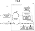
- FIG. 8 is a diagram illustrating a configuration of the kth calculation core 14-k.
- the kth calculation core 14-k has a receiving circuit 22, a calculation circuit 24, and a transmitting circuit 26.
- the receiving circuit 22 receives (N-M) first variables x i at the previous time step that are calculated by (P-1) calculation cores 14 other than the kth calculation core 14-k among P calculation cores 14, portion by portion sequentially, via the network 12.
- the receiving circuit 22 may receive all of N first variables x i including M first variables x i calculated by the kth calculation core 14-k, via the network 12.
- the calculation circuit 24 performs the interaction operation based on N first variables x i at the previous time step.
- the calculation circuit 24 thus can calculate M intermediate variables b i corresponding to M oscillators assigned to the kth calculation core 14-k.
- the calculation circuit 24 performs the time evolution operation, based on M intermediate variables b i obtained by performing the interaction operation, and M first variables x i at the previous time step and M second variables y i at the previous step corresponding to M oscillators assigned to the kth calculation core 14-k.
- the calculation circuit 24 thus can calculate M first variables x i at the target time step and M second variables y i at the target time step corresponding to M oscillators assigned to the kth calculation core 14-k.
- the transmitting circuit 26 transmits M first variables x i calculated by the calculation circuit 24 to (P-1) calculation cores 14 other than the kth calculation core 14-k among P calculation cores 14, via the network 12.
- the transmitting circuit 26 may transmit M first variables x i calculated by the calculation circuit 24 to P calculation cores 14 including the kth calculation core 14-k itself, via the network 12.
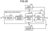
- the calculation circuit 24 includes a coefficient memory 32, a first memory 34, a second memory 36, an interaction circuit 38, a time evolution circuit 40, and a transfer circuit 42.
- the coefficient memory 32 stores an M ⁇ N submatrix containing M ⁇ N coupling coefficients J i,j that are used for calculating M intermediate variables b i corresponding to M oscillators assigned to the kth calculation core 14-k, among N ⁇ N coupling coefficients J i,j contained in the coupling matrix J.
- the coefficient memory 32 also stores M bias coefficients h i that are used for calculating M intermediate variables b i corresponding to M oscillators assigned to the kth calculation core 14-k, among N bias coefficients h i contained in the bias array h.
- the M ⁇ N submatrix containing M ⁇ N coupling coefficients J i,j and M bias coefficients h i stored in the coefficient memory 32 are preset by the management device 16.
- the first memory 34 stores M first variables x i corresponding to M oscillators assigned to the kth calculation core 14-k.
- M first variables x i stored in the first memory 34 are updated by the time evolution circuit 40 at each time step.
- M first variables x i stored in the first memory 34 are set to predetermined fixed values or random numbers in the initial state.
- the second memory 36 stores M second variables y i corresponding to M oscillators assigned to the kth calculation core 14-k.
- M second variables y i stored in the second memory 36 are updated by the time evolution circuit 40 at each time step.
- M second variables y i stored in the second memory 36 are set to predetermined fixed values or random numbers in the initial state.
- the interaction circuit 38 calculates M intermediate variables b i corresponding to M oscillators assigned to the kth calculation core 14-k, based on the M ⁇ N submatrix containing M ⁇ N coupling coefficients J i,j and M bias coefficients h i stored in the coefficient memory 32, and N first variables x i at the previous time step.
- the interaction circuit 38 calculates M intermediate variables b i corresponding to M oscillators assigned to the kth calculation core 14-k, based on M first variables x i at the previous time step calculated by the kth calculation core 14-k and (N-M) first variables x i at the previous time step calculated by (P-1) calculation cores 14 other than the kth calculation core 14-k.
- the interaction circuit 38 acquires N first variables x i portion by portion sequentially. Then, at each time step, the interaction circuit 38 calculates M intermediate variables b i by performing the interaction operation on N first variables x i portion by portion sequentially.
- the interaction circuit 38 also includes an intermediate variable memory 44.
- the intermediate variable memory 44 stores M intermediate variables b i under calculation while the interaction operation is performed on N first variables x i portion by portion sequentially.
- the interaction circuit 38 starts calculating M intermediate variables b i before the receiving circuit 22 completes reception of all of (N-M) first variables x i at the previous time step.
- the interaction circuit 38 thus can perform the interaction operation so as to overlap the receiving process of (N-M) first variables x i by the receiving circuit 22.
- the interaction circuit 38 supplies M intermediate variables b i to the time evolution circuit 40 after the interaction operation is finished.
- the time evolution circuit 40 calculates M first variables x i and M second variables y i at the target time step, based on M first variables x i at the previous time step stored in the first memory 34, M second variables y i at the previous time step stored in the second memory 36, and M intermediate variables b i calculated by the interaction circuit 38.
- the time evolution circuit 40 updates M first variables x i stored in the first memory 34 and M second variables y i stored in the second memory 36.
- the time evolution circuit 40 may calculate M first variables x i and M second variables y i by parallel processing by multiple circuits. For example, the time evolution circuit 40 may calculate M first variables x i and M second variables y i in M parallel by M circuits.
- the transfer circuit 42 transfers (N-M) first variables x i at the previous time step that are calculated by (P-1) calculation cores 14 other than the kth calculation core 14-k among P calculation cores 14, from the receiving circuit 22 to the interaction circuit 38.
- N first variables x i including M first variables x i calculated by the kth calculation core 14-k
- all of N first variables x i are transferred from the receiving circuit 22 to the interaction circuit 38.
- the transfer circuit 42 transfers M first variables x i calculated by the time evolution circuit 40 through a shortcut from the time evolution circuit 40 to the interaction circuit 38.
- the transfer circuit 42 also transfers M first variables x i calculated by the time evolution circuit 40, from the time evolution circuit 40 to the transmitting circuit 26.
- FIG. 9 is a diagram for explaining a sequential matrix multiplication process in the interaction circuit 38.
- the interaction circuit 38 performs a matrix multiplication process of N first variables x i and the corresponding submatrix in the M row by N column coupling matrix J, sequentially, at each time step.
- the interaction circuit 38 acquires N first variables x i at the previous time step, for each set of L first variables x i sequentially from the transfer circuit 42 (S121).
- L is an integer equal to or greater than 1 and less than N.
- L is a divisor of N.
- the interaction circuit 38 performs a product-sum operation of M ⁇ L coupling coefficients J i,j corresponding to the acquired L first variables x i in the M ⁇ N submatrix containing preset M ⁇ N coupling coefficients, and the acquired L first variables x i , row by row (S122). Then, every time L first variables x i are acquired, the interaction circuit 38 cumulatively adds the computation result of the product-sum operation for each row to the corresponding intermediate variable b i among M intermediate variables b i stored in the intermediate variable memory 44 (S123).
- the interaction circuit 38 outputs M intermediate variables b i to the time evolution circuit 40 after completing the product-sum operation corresponding to the last L first variables x i among N first variables x i (S124).
- the interaction circuit 38 thus can calculate M intermediate variables b i by performing the interaction operation on N first variables x i portion by portion sequentially.
- the time evolution circuit 40 acquires M intermediate variables b i output from the interaction circuit 38 and stores M intermediate variables b i in an internal buffer after the interaction operation is completed. The time evolution circuit 40 then performs the time evolution process, using M intermediate variables b i stored in the internal buffer.
- the buffer to store M intermediate variables b i after the interaction operation is completed may be provided in the interaction circuit 38 or may be provided in a path between the interaction circuit 38 and the time evolution circuit 40. Since the buffer to store M intermediate variables b i after the interaction operation is completed is provided in the calculation circuit 24, the interaction circuit 38 can start the interaction operation for calculating M intermediate variables b i at the next time step immediately after completing the interaction operation at the previous time step.
- the interaction circuit 38 erases M intermediate variables b i stored in the intermediate variable memory 44 before starting the computation using the initial L first variables x i . That is, the interaction circuit 38 sets the values of M intermediate variables b i to 0 before starting the computation using the initial L first variables x i .
- the interaction circuit 38 thus can store correct values in the intermediate variable memory 44.
- the interaction circuit 38 starts the computation using the initial L first variables x i among N first variables x i at the previous time step before the receiving circuit 22 completes reception of all of (N-M) first variables x i at the previous time step.
- the interaction circuit 38 thus can perform the interaction operation so as to overlap the receiving process of (N-M) first variables x i by the receiving circuit 22.
- the calculation time for each of P calculation cores 14 as described above is determined by computational resources.
- the communication time for reception and transmission is determined by the communication throughput and the communication latency that is the amount of data transferred per unit time.
- the total calculation time (time from inputting the initial first variable xi to completing the time evolution process) of each of P calculation cores 14 decreases as the time in which the calculation time and the communication time overlap increases.
- the interaction circuit 38 starts the interaction operation before each of P calculation cores 14 completes reception of all of (N-M) first variables x i at the previous time step calculated by the other calculation cores 14.
- Each of P calculation cores 14 performs the receiving process and the interaction operation in an overlapping manner. Therefore, the calculation device 10 according to the present arrangement can prevent the total calculation time of each of P calculation cores 14 from being prolonged due to communication overhead. With this configuration, the calculation device 10 according to the present arrangement can solve a large-scale combinatorial optimization problem fast.
- the calculation device 10 when the process time for the interaction operation is longer than the communication time, the calculation device 10 according to the present arrangement can completely eliminate the effect of the communication time on the total operating time of the calculation core 14.
- FIG. 10 is a diagram illustrating a first example of the network 12 connecting P calculation cores 14.
- the network 12 may, for example, be a crossbar network.
- the network 12 may be a shared bus.
- each of P calculation cores 14 can broadcast the first variables x i to each of P calculation cores 14 via the network 12. That is, each of P calculation cores 14 can directly receive the first variables x i from each of P calculation cores 14 without through the other calculation cores 14.
- the network 12 may include an Ethernet switch and an InfiniBand switch.
- the network 12 may have a router, a distribution device, or the like. In this case, the router or the distribution device can temporarily buffer the first variables x i transmitted from each of P calculation cores 14 and broadcast the buffered first variables x i to P calculation cores 14.
- the network 12 is not limited to a crossbar network or a shared bus and may be any other type of network that can broadcast the first variables x i to each of P calculation cores 14.
- the network 12 may be wiring that connects P calculation cores 14 to each other. In this case, the network 12 can significantly reduce the communication latency between the calculation cores 14.
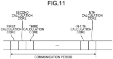
- FIG. 11 is a diagram illustrating the transmission timing of the first variables x i of each of P calculation cores 14 connected via the network 12 in the first example.
- the communication period in which N first variables x i are transmitted and received is divided into a plurality of time slots.
- Each of P calculation cores 14 is exclusively assigned one of the time slots.
- the transmitting circuit 26 of each of P calculation cores 14 then broadcasts the calculated M first variables x i to each of P calculation cores 14 via the network 12 in the assigned time slot. In the assigned time slot, the transmitting circuit 26 may broadcast the calculated M first variables x i to (P-1) calculation cores 14 excluding the transmitting calculation core 14 itself among P calculation cores 14.
- each of N first variables x i at each time step is assigned to one time slot among the time slots obtained by dividing the communication period and is transmitted via the network 12 in the assigned time slot.
- Each of P calculation cores 14 therefore can receive (N-M) first variables x i or N first variables x i portion by portion sequentially.
- FIG. 12 is a diagram illustrating a second example of the network 12 connecting P calculation cores 14.
- the network 12 may be a ring network that connects P calculation cores 14 in a ring form.
- the network 12 thus can cyclically transfer the first variables x i calculated by each of P calculation cores 14 to all of P calculation cores 14.
- P calculation cores 14 transmit and receive N first variables x i portion by portion in a bucket-brigade fashion, in the communication period in which N first variables x i at each time step are transmitted and received.
- the receiving circuit 22 of each of P calculation cores 14 receives (N-M) first variables x i excluding M first variables x i calculated by the calculation core 14 itself among N first variables x i , portion by portion, from the adjacent first calculation core 14 among P calculation cores 14, in the communication period.
- the receiving circuit 22 of each of P calculation cores 14 may receive all of N first variables x i including M first variables x i calculated by the calculation core 14 itself, from the adjacent first calculation core 14, in the communication period.
- the transmitting circuit 26 of each of P calculation cores 14 transmits M first variables x i calculated by the calculation core 14 itself to the adjacent second calculation core 14 different from the first calculation core 14 among P calculation cores 14, in the communication period. Furthermore, the transmitting circuit 26 of each of P calculation cores 14 transmits (N-M) first variables x i received from the first calculation core 14 to the second calculation core 14 in the communication period. The transmitting circuit 26 of each of P calculation cores 14 may transmit or may not necessarily transmit the first variables x i calculated by the second calculation core 14 to the second calculation core 14 when it receives the first variables x i calculated by the second calculation core 14, in the communication period.
- Such a network 12 allows the first variables x i transmitted from each of P calculation cores 14 to make a round so that each of P calculation cores 14 can receive N first variables x i . By transmitting in this way, each of P calculation cores 14 can receive (N-M) first variables x i or N first variables x i portion by portion sequentially.
- FIG. 13 is a diagram illustrating a third example of the network 12 connecting P calculation cores 14.
- the network 12 may be a plurality of ring networks that connect P calculation cores 14 in a ring form.
- the network 12 may include a first ring network and a second ring network.
- each of P calculation cores 14 performs full-duplex communication.
- the first ring network connects P calculation cores 14 along a ring-shaped first path and transfers data cyclically in a first direction of the first path.
- the second ring network connects P calculation cores 14 along the first path and transfers data cyclically in a second direction that is a direction opposite to the first direction of the first path.
- the first ring network and the second ring network transfer the same first variables x i .
- one of the first ring network and the second ring network may transfer a first variable group that is some of N first variables x i , and the other may transfer a second variable group other than the first variable group of N first variables x i .
- P calculation cores 14, connected by such a network 12, can increase the communication throughput compared with the second example.
- P calculation cores 14 can shorten the period from start of transmission of N first variables x i to completion of transmission of all of N first variables x i .
- P calculation cores 14 can complete transfer of all of N first variables x i with a small number of hops.
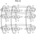
- FIG. 14 is a diagram illustrating a fourth example of the network 12 connecting P calculation cores 14.
- the network 12 may include three or more ring networks that connect P calculation cores 14 in a ring form.
- the network 12 may form connections by a plurality of ring networks in a two-dimensional torus shape.
- P calculation cores 14 repeat the process of transmitting a predetermined number of first variables x i to the adjacent calculation core 14 in a vertical ring network and then transmitting a predetermined number of first variables x i cyclically in one turn of the ring in a horizontal ring network.
- Each of P calculation cores 14, connected by such a network 12, can receive the first variables x i calculated by the other calculation cores 14 with a small number of hops. Therefore, P calculation cores 14, connected by such a network 12, can complete transfer of all of N first variables x i with a small number of hops.
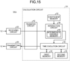
- FIG. 15 is a diagram illustrating a configuration of the calculation core 14 including the transfer circuit 42 in a first example.
- the transfer circuit 42 may have a configuration of the first example illustrated in FIG. 15 . That is, the transfer circuit 42 may be configured to transfer N first variables x i received by the receiving circuit 22 directly to the interaction circuit 38 and transfer M first variables x i calculated by the time evolution circuit 40 directly to the transmitting circuit 26.
- the receiving circuit 22 receives N first variables x i including M first variables x i calculated by the time evolution circuit 40 of the calculation core 14 itself, via the network 12.
- the interaction circuit 38 then sequentially acquires all of N first variables x i at the previous time step from the receiving circuit 22.
- FIG. 16 is a diagram illustrating a configuration of the calculation core 14 including the transfer circuit 42 in a second example.
- the transfer circuit 42 may have a configuration of the second example illustrated in FIG. 16 . That is, the transfer circuit 42 may have a configuration including a first multiplexer 46.
- the first multiplexer 46 time-multiplexes and supplies M first variables x i calculated by the time evolution circuit 40 and (N-M) first variables x i received by the receiving circuit 22 to the interaction circuit 38.
- the transfer circuit 42 in the second example also transfers M first variables x i calculated by the time evolution circuit 40 to the transmitting circuit 26.
- the first multiplexer 46 transfers M first variables x i calculated by the time evolution circuit 40 to the interaction circuit 38 before the initial first variable x i of (N-M) first variables x i is received by the receiving circuit 22.
- Such a transfer circuit 42 can shorten the time taken for the interaction circuit 38 to start operation. Such a transfer circuit 42 thus can expedite the completion of the computation by the interaction circuit 38.
- FIG. 17 is a diagram illustrating a configuration of the calculation core 14 including the transfer circuit 42 in a third example.
- the transfer circuit 42 may have a configuration of the third example illustrated in FIG. 17 . That is, the transfer circuit 42 may have a configuration including a second multiplexer 48. At each time step, the second multiplexer 48 time-multiplexes and supplies M first variables x i calculated by the time evolution circuit 40 and (N-M) first variables x i received by the receiving circuit 22 to the transmitting circuit 26. Furthermore, the transfer circuit 42 of the third example transfers N first variables x i received by the receiving circuit 22 directly to the interaction circuit 38.
- the receiving circuit 22 receives N first variables x i including M first variables x i calculated by the time evolution circuit 40 of the calculation core 14 itself, via the network 12.
- the interaction circuit 38 then sequentially acquires all of N first variables x i at the previous time step from the receiving circuit 22.
- FIG. 18 is a diagram illustrating a configuration of the calculation core 14 including the transfer circuit 42 in a fourth example.
- the transfer circuit 42 may have a configuration of the fourth example illustrated in FIG. 18 . That is, the transfer circuit 42 may have a configuration including a third multiplexer 50.
- the third multiplexer 50 time-multiplexes and supplies M first variables x i calculated by the time evolution circuit 40 and (N-M) first variables x i received by the receiving circuit 22 to both of the transmitting circuit 26 and the interaction circuit 38.
- the third multiplexer 50 starts transferring M first variables x i calculated by the time evolution circuit 40 to the interaction circuit 38 before the initial first variable x i of (N-M) first variables x i is received by the receiving circuit 22.
- a transfer circuit 42 can shorten the time taken for the interaction circuit 38 to start operation. Such a transfer circuit 42 thus can expedite the completion of the computation by the interaction circuit 38.
- FIG. 19 is a diagram illustrating process timings of two calculation cores 14 each including the transfer circuit 42 in the third example.
- FIG. 20 is a diagram illustrating the details of process timing of one calculation core 14 including the transfer circuit 42 in the third example.
- FIG. 19 illustrates an example in which all the calculation cores 14 operate at the same timing, the operating timing may be shifted for each calculation core 14.
- the timing chart in FIG. 20 depicts timings assuming that the latency for data movement in the calculation core 14, the latency for data to pass through the receiving circuit 22, and the latency for data to pass through the transmitting circuit 26 are zero.
- the receiving circuit 22 then temporarily buffers the received M first variables x i and outputs the buffered first variables x i to the interaction circuit 38.
- the interaction circuit 38 then acquires N first variables x i M by M sequentially from the receiving circuit 22.
- the interaction circuit 38 After all of N first variables x i are received, the interaction circuit 38 outputs the calculated M intermediate variables b i to the time evolution circuit 40. The time evolution circuit 40 then calculates M first variables x i and thereafter outputs the calculated M first variables x i to the transmitting circuit 26. The transmitting circuit 26 transmits M first variables x i received from the time evolution circuit 40 to the adjacent calculation core 14 via the network 12.
- the transmitting circuit 26 receives the received M first variables x i and transmits the received M first variables x i to the adjacent calculation core 14.
- P calculation cores 14 thus can transmit and receive N first variables x i in a bucket-brigade fashion.
- the receiving circuit 22 receives the initial M first variables x i after the communication latency between the calculation cores 14 has passed since M first variables x i calculated by the time evolution circuit 40 are transmitted via the network 12.
- the interaction circuit 38 starts the interaction operation for the initial M first variables x i after the communication latency between the calculation cores 14 has passed in the process at each time step.
- L comm represents the communication latency between the calculation cores 14.
- L JX represents the time from when the acquisition of all N first variables x i is completed to when the interaction circuit 38 outputs M intermediate variables b i .
- L TE represents the time from when the interaction circuit 38 outputs M intermediate variables b i to when the time evolution circuit 40 outputs M first variables x i .
- P c represents the processing speed from when the time evolution circuit 40 acquires M intermediate variables b i to when M first variables x i are output and from when the receiving circuit 22 acquires the initial N first variables x i to when the interaction circuit 38 outputs M intermediate variables b i .
- FIG. 21 is a diagram illustrating process timings of two calculation cores 14 each including the transfer circuit 42 in the fourth example.
- FIG. 22 is a diagram illustrating the details of process timing of one calculation core 14 including the transfer circuit 42 in the fourth example.
- FIG. 21 illustrates an example in which all the calculation cores 14 operate at the same timing, the operating timing may be shifted for each calculation core 14.
- the timing chart in FIG. 22 depicts timings assuming that the latency for data movement in the calculation core 14, the latency for data to pass through the receiving circuit 22, and the latency for data to pass through the transmitting circuit 26 are zero.
- the interaction circuit 38 acquires M first variables x i output by the time evolution circuit 40 directly from the time evolution circuit 40 without going through the network 12.
- the interaction circuit 38 therefore can start the computation process on M first variables x i output by the time evolution circuit 40 before the initial M first variables x i are received from the adjacent calculation core 14 in the process at each time step.
- the receiving circuit 22 has an internal buffer in the inside and buffers the received M first variables x i until the interaction operation on the previous M first variables x i by the interaction circuit 38 is completed.
- the calculation core 14 including the transfer circuit 42 in the fourth example can reduce the process time per time step, compared with the case including the transfer circuit 42 in the third example.
- FIG. 23 is a diagram illustrating pseudocode 52 describing the process in the calculation core 14 including the transfer circuit 42 in the fourth example.
- FIG. 24 is a flowchart illustrating the process in the calculation core 14 when the process is performed according to the pseudocode 52.
- the calculation core 14 performs the process illustrated FIG. 23 and FIG. 24 .
- t is a variable representing time.
- ⁇ t is a constant representing a time step.
- i is an index that identifies M oscillators assigned to the calculation core 14 among N oscillators.
- j is an index that identifies N oscillators.
- b i is an intermediate variable stored in the intermediate variable memory 44 and being under calculation in the interaction operation.
- b' i is an intermediate variable that is stored in a buffer provided in the interaction circuit 38, in the time evolution circuit 40, or between the interaction circuit 38 and the time evolution circuit 40 and is the final computation result of the interaction operation.
- x j is the first variable.
- x' j is the first variable obtained by multiplying x j by a constant ( ⁇ t ⁇ c).
- y j is the second variable.
- the calculation core 14 initializes parameters.
- S201 corresponds to the process from lines 1 to 6 of the pseudocode 52. Specifically, in line 1, the calculation core 14 sets t to 0. In line 2, the calculation core 14 divides N by P to calculate M representing the number of virtual oscillators assigned to the calculation core 14. In lines 3 to 6, the calculation core 14 initializes each of M b 1 to b M and M b' 1 to b' M to 0.
- the calculation core 14 performs the loop between S202 and S214.
- the loop between S202 and S214 corresponds to lines 7 to 31 of the pseudocode 52.
- the calculation core 14 substitutes 0 for ncycle that is a variable representing the number of iterations, adds 1 to ncycle for each iteration, and exits the loop when ncycle is equal to or greater than Nstep representing the preset number of times of iterations.
- the calculation core 14 performs a loop between S203 and S211.
- the loop process between S203 and S211 corresponds to lines 8 to 25 of the pseudocode 52.
- the calculation core 14 substitutes 1 for j in the first loop, adds 1 to j for each iteration, and exits the loop when j is greater than N.
- the calculation core 14 determines whether the time evolution circuit 40 is in the process of outputting x' i .
- S204 corresponds to line 9 of the pseudocode 52. Specifically, the calculation core 14 determines whether j is less than or equal to M.
- the calculation core 14 receives x' i at S205.
- S205 corresponds to line 16 of the pseudocode 52. Specifically, the calculation core 14 substitutes the value received by the receiving circuit 22 for x' j .
- the time evolution circuit 40 updates y j , x j , and x' j .
- S206 corresponds to lines 12, 13, and 14 of the pseudocode 52.
- the time evolution circuit 40 updates y j by the FX function that updates y j with x j .
- the time evolution circuit 40 updates x j by the FY function that updates x j with y j .
- the time evolution circuit 40 calculates x' j by multiplying x j by dt ⁇ c.
- the calculation core 14 performs S208 and S209 to S210 in parallel.
- the calculation core 14 multiplies x' j received at S205 by the corresponding coupling coefficient J i,j and cumulatively adds the multiplication value to the corresponding b i .
- S208 corresponds to lines 18 to 21 of the pseudocode 52. Specifically, the calculation core 14 substitutes 1 for i in line 18, adds 1 to i every time the cumulative addition is performed, and terminates the cumulative addition process when i becomes greater than M.
- the calculation core 14 determines whether x' j has reached the adjacent calculation core 14 that is the destination of x' j . If x' j has not reached (No at S209), at S210, the calculation core 14 transmits x' j to the adjacent calculation core 14. If it has reached (Yes at S209), the calculation core 14 skips the process at S210. S209 to S210 correspond to lines 22 to 24 of the pseudocode 52. Specifically, if j is less than or equal to M ⁇ (P-1), the calculation core 14 transmits x' j to the adjacent calculation core 14 .
- the calculation core 14 proceeds to S212.
- the calculation core 14 updates t by adding ⁇ t to t. S212 corresponds to line 26 of the pseudocode 52.
- the calculation core 14 updates each of M b' i and M b i .
- the calculation core 14 thus can transfer the value stored in the intermediate variable memory 44 to the buffer that stores the intermediate variable b' i that is the final computation result of the interaction operation.
- the calculation core 14 then repeats the loop between S202 and S214 Nstep times and thereafter terminates the process.
- FIG. 25 is a diagram illustrating a configuration of the interaction circuit 38 according to a first example.
- the interaction circuit 38 according to the first example is a configuration in which each of P calculation cores 14 receives N first variables x 1 to x N sequentially in units of L first variables x i (L is equal to or greater than 1 and less than N). This is applicable to the interaction circuit 38 according to the following second and third examples.
- the interaction circuit 38 according to the first to third examples performs the matrix multiplication process as the interaction operation and does not perform the bias addition process. That is, the interaction circuit 38 according to the first to third examples does not add the bias coefficient h i to the intermediate variable b i .
- the interaction circuit 38 has M product-sum circuits 60-1 to 60-M, M cumulative sum circuits 62-1 to 62-M, and an aggregation circuit 64.
- M product-sum circuits 60-1 to 60-M correspond one-to-one with M oscillators assigned to the calculation core 14.
- Each of M product-sum circuits 60-1 to 60-M includes L multipliers 66 and a first adder 68. Every time the interaction circuit 38 acquires a set of L first variables x (A-1)L+1 to x AL (A is an integer number not less than 1), each of L multipliers 66 multiplies the corresponding one first variable x i of L first variables x (A-1)L+1 to x AL by the corresponding coupling coefficient J i,j contained in the coupling matrix J stored in the coefficient memory 32.
- the first adder 68 adds the multiplication results of all of L multipliers 66.
- the first adder 68 then outputs a product-sum value by adding the multiplication results of all of L multipliers 66.
- Each of M product-sum circuits 60-1 to 60-M according to the first example is configured to perform the product-sum operation on L first variables x (A-1)L+1 to x AL in one clock cycle, but the arrangements are not limited to this configuration.
- each of M product-sum circuits 60-1 to 60-M according to the first example may be a circuit that performs the product-sum operation on L first variables x (A-1)L+1 to x AL in a plurality of clocks.
- M cumulative sum circuits 62-1 to 62-M correspond one-to-one with M oscillators assigned to the calculation core 14.
- Each of M cumulative sum circuits 62-1 to 62-M includes a second adder 70 and a register 72. Every time a set of L first variables x (A-1)L+1 to x AL is acquired, each of M cumulative sum circuits 62-1 to 62-M acquires a product-sum value from the corresponding one product-sum circuit 60 among M product-sum circuits 60-1 to 60-M. Every time a product-sum value is acquired from the corresponding product-sum circuit 60, the second adder 70 adds the acquired product-sum value to the value stored in the register 72 and writes the addition result in the register 72 again.
- the register 72 stores a value and has the stored value updated every time a product-sum value is acquired from the corresponding product-sum circuit 60.
- the register 72 included in each of M cumulative sum circuits 62-1 to 62-M functions as the intermediate variable memory 44. That is, in this example, the intermediate variable memory 44 includes M registers 72.
- the register 72 included in each of M cumulative sum circuits 62-1 to 62-M stores M intermediate variables b i under calculation that are calculated while the interaction operation is performed on N first variables x i portion by portion sequentially.
- the aggregation circuit 64 After the computation on all of N first variables x i is completed, the aggregation circuit 64 reads the values stored in M registers 72 functioning as the intermediate variable memory 44 and supplies the read values to the time evolution circuit 40 as M intermediate variables b 1 to b M . In this case, at each time step, the aggregation circuit 64 time-divisionally aggregates and supplies each of M intermediate variables b 1 to b M stored in M registers 72 functioning as the intermediate variable memory 44, to the time evolution circuit 40.
- the interaction circuit 38 may include a plurality of aggregation circuits 64.
- each of the aggregation circuits 64 selects corresponding some of intermediate variables b i among M intermediate variables b 1 to b M and supplies the selected some to a circuit among the circuits included in the time evolution circuit 40.
- FIG. 26 is a diagram illustrating a computation process of the interaction circuit 38 according to the first example illustrated in FIG. 25 . Every time L first variables x i are acquired, the interaction circuit 38 according to the first example having the configuration illustrated in FIG. 25 can perform the product-sum operation of an M row by L column submatrix corresponding to the acquired L first variables x i among the preset M row by N column coefficients, and the acquired L first variables x i , row by row.
- the interaction circuit 38 according to the first example then cumulatively adds the product-sum value every time L first variables x i are acquired.
- the interaction circuit 38 according to the first example thus can store M intermediate variables b i under calculation that are calculated while the product-sum operation is performed on N first variables x i L by L sequentially, in the intermediate variable memory 44.
- FIG. 27 is a diagram illustrating a configuration of the interaction circuit 38 according to a second example.
- the interaction circuit 38 according to the second example includes (M/2) product-sum circuits 60-1 to 60-M/2, (M/2) cumulative sum circuits 62-1 to 62-(M/2), and an aggregation circuit 64.
- Each of (M/2) product-sum circuits 60-1 to 60-M/2 corresponds exclusively to two of M oscillators assigned to the calculation core 14.
- Each of (M/2) product-sum circuits 60-1 to 60-M/2 has a configuration similar to that of the product-sum circuit 60 according to the first example. However, each of (M/2) product-sum circuits 60-1 to 60-M/2 sequentially outputs two product-sum values every time a set of L first variables x (A-1)L+1 to x AL are acquired. Specifically, in the first cycle, each of (M/2) product-sum circuits 60-1 to 60-M/2 performs the product-sum operation of L first variables x (A-1)L+1 to x AL and L coupling coefficients J i,j included in the row corresponding to one of the two corresponding oscillators in the coupling matrix J.
- each of (M/2) product-sum circuits 60-1 to 60-M/2 performs the product-sum operation of L first variables x (A-1)L+1 to x AL and L coupling coefficients J i,j included in the row corresponding to the other of the two corresponding oscillators in the coupling matrix J.
- Each of (M/2) cumulative sum circuits 62-1 to 62-M/2 corresponds exclusively to two of M oscillators assigned to the calculation core 14.
- Each of (M/2) cumulative sum circuits 62-1 to 62-M/2 includes a second adder 70, a first register 72-1, and a second register 72-2. Every time a set of L first variables x (A-1)L+1 to x AL is acquired, each of (M/2) product-sum circuits 60-1 to 60-M/2 sequentially acquires two product-sum values from the corresponding one product-sum circuit 60 among (M/2) product-sum circuits 60-1 to 60-M/2. In the first cycle, the second adder 70 adds the acquired product-sum value to the value stored in the first register 72-1 and writes the addition result in the first register 72-1 again. In the second cycle, the second adder 70 adds the acquired product-sum value to the value stored in the second register 72-2 and writes the addition result in the second register 72-2 again.
- the first register 72-1 and the second register 72-2 included in each of (M/2) cumulative sum circuits 62-1 to 62-M/2 function as the intermediate variable memory 44.
- the aggregation circuit 64 After the computation on all of N first variables x i is completed, the aggregation circuit 64 reads the values stored in the first register 72-1 and the second register 72-2 functioning as the intermediate variable memory 44 and supplies the read values to the time evolution circuit 40 as M intermediate variables b 1 to b M .
- FIG. 28 is a diagram illustrating a computation process of the interaction circuit 38 according to the second example illustrated in FIG. 27 .
- the interaction circuit 38 according to the second example having the configuration illustrated in FIG. 27 performs the product-sum operation process of two cycles every time L first variables x i are acquired. In each cycle, the interaction circuit 38 can perform the product-sum operation of a (M/2) row by L column submatrix corresponding to the acquired L first variables x i among the preset M row by N column coefficients, and the acquired L first variables x i , row by row.
- the interaction circuit 38 according to the second example then cumulatively adds two product-sum values as different intermediate variables b i every time L first variables x i are acquired. Therefore, the interaction circuit 38 according to the second example stores M intermediate variables b i under calculation that are calculated while product-sum operation is performed on N first variables x i L by L sequentially, in the intermediate variable memory 44.
- the interaction circuit 38 includes (M/2) product-sum circuits 60-1 to 60-M/2 and (M/2) cumulative sum circuits 62-1 to 62-M/2 but may include (M/4) product-sum circuits 60-1 to 60-M/4 and (M/4) cumulative sum circuits 62-1 to 62-M/4.
- each of (M/4) product-sum circuits 60-1 to 60-M/4 performs the product-sum operation process of four cycles every time L first variables x i are acquired.
- each of (M/4) cumulative sum circuits 62-1 to 62-M/4 includes a first register 72-1 to a fourth register 72-4.
- the interaction circuit 38 may include any other number of product-sum circuits 60 and cumulative sum circuits 62.
- FIG. 29 is a diagram illustrating a configuration of the interaction circuit 38 according to a third example.
- the interaction circuit 38 according to the third example includes M product-sum circuits 60-1 to 60-M and M cumulative sum circuits 62-1 to 62-M.
- the interaction circuit 38 according to the third example does not include the aggregation circuit 64, compared with the interaction circuit 38 according to the first example.
- M registers 72 included in M cumulative sum circuits 62-1 to 62-M are connected in series.
- M registers 72 function as a shift register that transfers the stored value to the adjacent register 72 in the series direction.
- the interaction circuit 38 allows M registers 72 to function as a shift register and sequentially supplies M intermediate variables b 1 to b M to the time evolution circuit 40.
- M registers 72 may be arranged in a plurality of columns and connected for each column. In this case, M registers 72 function as a plurality of shift registers that transfer the stored value to the adjacent register in the series direction for each column. After the computation on all of the N first variables x i is completed, the interaction circuit 38 allows M registers 72 to function as a plurality of shift registers and supplies M intermediate variables b 1 to b M to the time evolution circuit 40 sequentially in the predetermined degree of parallelism.
- the interaction circuit 38 can sequentially supply M intermediate variables b 1 to b M to the time evolution circuit 40 after the interaction operation is completed.
- the interaction circuit 38 may be configured such that all of the first registers 72-1 and the second registers 72-2 included in (M/2) cumulative sum circuits 62-1 to 62-M/2 in the second example are connected in series to function as a shift register.
- FIG. 30 is a diagram illustrating a configuration of the time evolution circuit 40 together with the first memory 34 and the second memory 36.
- the time evolution circuit 40 includes a buffer circuit 82, a preprocessing circuit 84, a function computation circuit 86, and a postprocessing circuit 88.
- the buffer circuit 82 acquires and stores M intermediate variables b i output from the interaction circuit 38.
- the buffer circuit 82 may be provided on the outside of the time evolution circuit 40 or may be provided at the output stage of the interaction circuit 38.
- the preprocessing circuit 84 performs a predetermined computation process on each of M intermediate variables b i stored in the buffer circuit 82. For example, the preprocessing circuit 84 multiplies each of M intermediate variables b i by a coefficient or adds or subtracts a constant. When a computation process is not performed on each of M intermediate variables b i , the time evolution circuit 40 does not include the preprocessing circuit 84.
- the function computation circuit 86 acquires M intermediate variables b i subjected to a predetermined computation process by the preprocessing circuit 84.
- the function computation circuit 86 acquires the intermediate variable b i from the buffer circuit 82.
- the function computation circuit 86 reads the first variable x i at the previous time step corresponding to each of M intermediate variables b i , from the first memory 34. In addition, the function computation circuit 86 reads the second variable y i at the previous time step corresponding to each of M intermediate variables b i , from the second memory 36. The function computation circuit 86 then calculates M first variables x i and M second variables y i at the target time step.
- the function computation circuit 86 calculates the second variable y i at the target time step by performing the computation given by Equation (6) using the intermediate variable b i and the first variable x i at the previous time step.
- y i y i + FX x i + dt ⁇ c ⁇ b i
- FX x i dt ⁇ ⁇ D + p t ⁇ Kx i 2 x i
- the function computation circuit 86 calculates the first variable x i at the target time step by performing the computation given by Equation (7) using the second variable y i at the target time step.
- the function computation circuit 86 may reverse the order of computation of Equation (6) and Equation (7). That is, the function computation circuit 86 may calculate the first variable x i at the target time step by performing the computation given by Equation (7) using the second variable y i at the previous time step and then calculate the second variable y i at the target time step by performing the computation given by Equation (6) using the intermediate variable b i and the first variable x i at the target time step.
- the function computation circuit 86 may repeat the momentum update process using FX(x i ) in Equation (6) and the position update process using FY(y i ) in Equation (7) alternately a predetermined number of times, during the process in one time step. In this case, the function computation circuit 86 sets dt in FX(x i ) and FY(y i ) to a minute time ⁇ t shorter than the time step.
- the momentum update process is a process of calculating the difference of momentum ⁇ y i after a minute time ⁇ t by computing FX(x i ) and adding the calculated difference of momentum ⁇ y i to the second variable y i .
- the position update process is a process of calculating the difference of position ⁇ x i after a minute time ⁇ t by calculating FY(y i ) and adding the calculated difference of position ⁇ x i to the first variable x i .
- the function computation circuit 86 repeats the momentum update process and the position update process, the number of times obtained by dividing dt by ⁇ t.
- the function computation circuit 86 may set K in Equation (6) to 0 and limit the range of the first variable x i to within a predetermined range (for example, -1 through +1, both inclusive).
- the function computation circuit 86 may binarize the value of the first variable x i by the signum function sgn(x i ) in the computation at each time step.
- the postprocessing circuit 88 acquires M first variables x i and M second variables y i calculated by the function computation circuit 86.
- the postprocessing circuit 88 performs a predetermined computation process or a predetermined manipulation on each of M first variables x i and each of M second variables y i .
- the postprocessing circuit 88 may perform a predetermined manipulation (for example, manipulations such as adding a predetermined value, multiplying a predetermined value, and adding or multiplying a random number) on one or both of M first variables x i and M second variables y i under a predetermined condition.
- the postprocessing circuit 88 need not perform any computation or manipulation on each of M first variables x i and each of M second variables y i .
- the postprocessing circuit 88 then stores M first variables x i at the target time step in the first memory 34.
- the postprocessing circuit 88 also stores M second variables y i at the target time step in the second memory 36.
- the postprocessing circuit 88 supplies M first variables x i at the target time step to the transfer circuit 42.
- the postprocessing circuit 88 thus can supply the calculated M first variables x i to the other calculation cores 14 and the interaction circuit 38.
- the function computation circuit 86 may multiply each of M first variables x i to be supplied to the transfer circuit 42 by c and ⁇ t, before the interaction operation.
- the function computation circuit 86 thus can perform the process of multiplying dt ⁇ c in Equation (6), prior to the interaction operation.
- FIG. 31 is a diagram illustrating a configuration of a calculation server 103.
- Each of P calculation cores 14 may be an information processing device such as the calculation server 103.
- the calculation server 103 includes, for example, a communication circuit 131, a memory 132, processors 133a to 133d, a storage 134, and a host bus adapter 135.
- the communication circuit 131, the memory 132, the processors 133a to 133d, the storage 134, and the host bus adapter 135 are connected to each other through a bus 136.
- the communication circuit 131 transmits/receives data to/from the devices connected to a network 102.
- the communication circuit 131 is, for example, a network interface card (NIC) for a wired LAN.
- the communication circuit 131 may be any other kind of communication circuit, such as a wireless LAN.
- the memory 132 is a memory accessible by the processors 133a to 133d.
- the memory 132 is, for example, a volatile memory such as a DRAM and an SRAM.
- the memory 132 may include any other kind of memory such as a nonvolatile memory.
- the processors 133a to 133d share data through the memory 132.
- the memory 132 is not necessarily configured with all of the memories of the calculation server 103. For example, some memories of the calculation server 103 may be local memories accessible only by any one of the processors 133a to 133d.
- the processors 133a to 133d are electronic circuits that perform a calculation process.
- the processors 133a to 133d may be, for example, CPUs, GPUs, FPGAs, or ASICs, or may be a combination thereof.
- the processors 133a to 133d may be CPU cores or CPU threads. When the processors 133a to 133d are CPUs, the number of sockets included in the calculation server 103 is not limited.
- the processors 133a to 133d may be connected to any other components of the calculation server 103 through a bus such as PCI Express.
- the calculation server 103 includes four processors 133a to 133d.
- the number of processors included in one calculation server 103 is not limited to four.
- the storage 134 stores a computer program for the calculation server 103 and a variety of data including data necessary for executing the computer program and data generated by the computer program.
- the computer program includes both an OS and an application.
- the storage 134 may be a volatile memory and a nonvolatile memory, or a combination thereof.
- the volatile memory is, for example, a DRAM or an SRAM.
- the nonvolatile memory is, for example, a NAND flash memory, an NOR flash memory, an ReR_AM, or an MR_AM.
- the storage 134 may include a hard disk, an optical disk, a magnetic tape, or an external storage device.
- the host bus adapter 135 implements data communication with other calculation servers 103.
- the host bus adapter 135 is connected to a switch 105 through a cable 104.
- the host bus adapter 135 is, for example, a host channel adapter (HCA).
- HCA host channel adapter
- the host bus adapter 135, the cable 104, and the switch 105 form an interconnection that can achieve a high throughput and thereby can improve the speed of parallel calculation processing.
Landscapes
- Engineering & Computer Science (AREA)
- Physics & Mathematics (AREA)
- General Physics & Mathematics (AREA)
- Theoretical Computer Science (AREA)
- Mathematical Physics (AREA)
- Data Mining & Analysis (AREA)
- Software Systems (AREA)
- Computational Mathematics (AREA)
- Mathematical Analysis (AREA)
- Mathematical Optimization (AREA)
- Pure & Applied Mathematics (AREA)
- General Engineering & Computer Science (AREA)
- Computing Systems (AREA)
- Algebra (AREA)
- Evolutionary Computation (AREA)
- Artificial Intelligence (AREA)
- Databases & Information Systems (AREA)
- Nonlinear Science (AREA)
- Probability & Statistics with Applications (AREA)
- Operations Research (AREA)
- Computational Linguistics (AREA)
- Complex Calculations (AREA)
- Multi Processors (AREA)
- Management, Administration, Business Operations System, And Electronic Commerce (AREA)
- Computer Hardware Design (AREA)
- Geometry (AREA)
Claims (14)
- Dispositif de calcul (10) configuré pour produire une solution d'un problème d'optimisation avec N variables discrètes, où N est un nombre entier supérieur à 2, le dispositif de calcul (10) comprenant :un réseau (12) ; etP noyaux de calcul (14), chacun connecté au réseau (12) et chacun mis en oeuvre par un circuit matériel, où P est un nombre entier égal ou supérieur à 2 et inférieur à N, dans lequelchacun des P noyaux de calcul (14) se voit exclusivement attribué à certains des N oscillateurs virtuels,les N oscillateurs virtuels correspondent un à un aux N variables discrètes et changent virtuellement de position et d'impulsion dans le temps dans une direction unidimensionnelle,les P noyaux de calcul (14) sont configurés pour calculer N premières variables représentant la position et N deuxièmes variables représentant l'impulsion des N oscillateurs virtuels, séquentiellement pour chacun des pas de temps allant d'un temps initial à un temps final,les P noyaux de calcul (14) sont configurés pour produire des valeurs basées sur les N premières variables au temps final en tant que valeurs basées sur la solution du problème d'optimisation,un k-ième noyau de calcul (14) parmi les P noyaux de calcul, où k est un nombre entier égal ou supérieur à 1 et inférieur à P,se voit attribué à M oscillateurs virtuels parmi les N oscillateurs virtuels, où M est un nombre entier égal ou supérieur à 1 et inférieur à N, età chacun des pas de temps, est configuré pour calculer M premières variables correspondant aux M oscillateurs virtuels assignés parmi les N premières variables et M deuxièmes variables correspondant aux M oscillateurs virtuels,le k-ième noyau de calcul (14) inclut :un circuit de réception (22) configuré pour recevoir, à chacun des pas de temps, N-M premières variables à un pas de temps précédent calculées par P-1 noyaux de calcul autres que le k-ième noyau de calcul parmi les P noyaux de calcul (14), partie par partie séquentiellement, via le réseau (12) ;un circuit d'interaction (38) configuré pour calculer, à chacun des pas de temps, M variables intermédiaires correspondant aux M oscillateurs virtuels, sur la base des N premières variables au pas de temps précédent ;un circuit d'évolution temporelle (40) configuré pour calculer, à chacun des pas de temps, les M premières variables et les M deuxièmes variables à un pas de temps cible sur la base des M premières variables au pas de temps précédent, les M deuxièmes variables au pas de temps précédent et les M variables intermédiaires ; etun circuit de transmission (26) configuré pour transmettre, à chacun des pas de temps, les M premières variables calculées par le circuit d'évolution temporelle (40) aux noyaux de calcul P-1 (14) via le réseau (12),le circuit d'interaction (38) inclut une mémoire de variables intermédiaires (44) configurée pour stocker les M variables intermédiaires en cours de calcul,à chacun des pas de temps, le circuit d'interaction (38) est configuré pour commencer le calcul des M variables intermédiaires avant que le circuit de réception (22) n'achève la réception de toutes les N-M premières variables au pas de temps précédent,la mémoire des variables intermédiaires (44) inclut M registres (72) correspondant aux M variables intermédiaires,chacun des M registres (72) est écrit avec une valeur en cours de calcul dans une variable intermédiaire correspondante,les M registres (72) sont connectés en série pour fonctionner comme un registre à décalage configuré pour transférer une valeur stockée à un registre adjacent dans une direction de la série, ou sont disposés en une pluralité de colonnes et connectés pour chaque colonne pour fonctionner comme une pluralité de registres à décalage configurés pour transférer une valeur stockée à un registre adjacent dans une direction de la série pour chaque colonne, etle circuit d'interaction (38) est configuré pour permettre aux M registres de fonctionner comme le registre à décalage ou aux registres à décalage de fournir les M variables intermédiaires au circuit d'évolution temporelle (40).
- Dispositif de calcul (10) selon la revendication 1, dans lequel à chacun des pas de temps, le circuit d'interaction (38) est configuré pour :acquérir certaines des N premières variables au pas de temps précédent, partie par partie séquentiellement ;à chaque acquisition des certaines des premières variables, effectuer une opération produit-somme de certains des coefficients de couplage correspondant aux certaines variables acquises des premières variables dans une sous-matrice M × N prédéfinie et aux certaines variables acquises des premières variables, ligne par ligne ; età chaque acquisition des certaines des premières variables, ajouter cumulativement chacun des résultats de calcul de l'opération produit-somme pour chaque ligne à une variable intermédiaire correspondante parmi les M variables intermédiaires stockées dans la mémoire de variables intermédiaires (44), età chacun des pas de temps, le circuit d'interaction (38) est configuré pour commencer le calcul en utilisant les certaines des premières variables parmi les N premières variables du pas de temps précédent avant que le circuit de réception (22) n'achève la réception de toutes les N-M premières variables du pas de temps précédent.
- Dispositif de calcul (10) selon la revendication 2, dans lequel le k-ième noyau de calcul (14) inclut en outre une mémoire de coefficient (32) configurée pour stocker la sous-matrice M × N prédéfinie.
- Dispositif de calcul (10) selon la revendication 2 ou 3, dans lequel le k-ième noyau de calcul (14) inclut en outre :une première mémoire (34) configurée pour stocker les M premières variables ; etune deuxième mémoire (36) configurée pour stocker les M deuxièmes variables, età chacun des pas de temps, le circuit d'évolution temporelle (40) est configuré pour mettre à jour les M premières variables stockées dans la première mémoire (34) et mettre à jour les M deuxièmes variables stockées dans la deuxième mémoire (36).
- Dispositif de calcul (10) selon l'une quelconque des revendications 2 à 4, dans lequel, à chacun des pas de temps, le circuit d'interaction (38) est configuré pour produire les M variables intermédiaires au circuit d'évolution temporelle (40) après avoir achevé l'opération produit-somme correspondant à certaines dernières des premières variables parmi les N premières variables.
- Dispositif de calcul (10) selon la revendication 5, dans lequel à chacun des pas de temps, le circuit d'interaction (38) est configuré pour effacer les M variables intermédiaires stockées dans la mémoire de variables intermédiaires (44) avant de commencer le calcul en utilisant les certaines des premières variables.
- Dispositif de calcul (10) selon l'une quelconque des revendications 1 à 6, dans lequeldans une période de communication au cours de laquelle les N premières variables à chaque pas de temps sont transmises et reçues, chacun des P noyaux de calcul (14) se voit attribuer un créneau temporel parmi une pluralité de créneaux temporels obtenus en divisant la période de communication, etle circuit de transmission (26) est configuré pour diffuser les M premières variables calculées aux P-1 noyaux de calcul (14) via le réseau (12) dans le créneau temporel attribué.
- Dispositif de calcul (10) selon la revendication 7, dans lequelle circuit de réception (22) est configuré pour recevoir les M premières variables calculées par le circuit d'évolution temporelle (40) via le réseau (12), età chacun des pas de temps, le circuit d'interaction (38) est configuré pour acquérir séquentiellement toutes les N premières variables du pas de temps précédent auprès du circuit de réception (22).
- Dispositif de calcul (10) selon la revendication 7, dans lequelle k-ième noyau de calcul (14) inclut en outre un multiplexeur (46) configuré pour effectuer un multiplexage temporel et fournir les M premières variables calculées par le circuit d'évolution temporelle (40) et les N-M premières variables reçues par le circuit de réception (22) au circuit d'interaction (38), età chacun des pas de temps, le circuit d'interaction (38) est configuré pour acquérir séquentiellement toutes les N premières variables du pas de temps précédent à partir du multiplexeur (46).
- Dispositif de calcul (10) selon l'une quelconque des revendications 1 à 6, dans lequelle réseau (12) relie les noyaux de calcul P (14) sous forme d'anneau, etau cours d'une période de communication durant laquelle les N premières variables de chaque pas de temps sont transmises et reçues, pour chacun des P noyaux de calcul (14), le circuit de réception (22) reçoit des premières variables d'un premier noyau de calcul (14) directement connecté par le réseau (12) parmi les P noyaux de calcul (14) et le circuit de transmission (26) transmet des premières variables, qui sont mises en mémoire tampon, à un deuxième noyau de calcul (14) directement connecté par le réseau (12) qui est autre que le premier noyau de calcul (14) parmi les P noyaux de calcul (14).
- Dispositif de calcul (10) selon la revendication 10, dans lequelle k-ième noyau de calcul (14) inclut en outre un multiplexeur (48) configuré pour effectuer un multiplexage temporel et fournir les M premières variables calculées par le circuit d'évolution temporelle (40) et les N-M premières variables reçues par le circuit de réception (22) au circuit de transmission (26),le circuit de réception (22) est configuré pour recevoir toutes les N premières variables au pas de temps précédent via le réseau (12), età chacun des pas de temps, le circuit d'interaction (38) est configuré pour acquérir séquentiellement toutes les N premières variables du pas de temps précédent auprès du circuit de réception (22).
- Dispositif de calcul (10) selon la revendication 10, dans lequelle k-ième noyau de calcul (14) inclut en outre un multiplexeur (50) configuré pour effectuer un multiplexage temporel et fournir les M premières variables calculées par le circuit d'évolution temporelle (40) et les N-M premières variables reçues par le circuit de réception (22) au circuit de transmission (26), età chacun des pas de temps, le circuit d'interaction (38) est configuré pour acquérir séquentiellement les N premières variables du pas de temps précédent à partir du multiplexeur (50).
- Dispositif de calcul (10) selon l'une quelconque des revendications 1 à 12, dans lequel le circuit d'interaction (38) inclut en outre un circuit d'agrégation (64) configuré pour agréger de manière temporellement fractionnée et fournir au circuit d'évolution temporelle (40), à chacun des pas de temps, les M variables intermédiaires stockées dans la mémoire de variables intermédiaires (44).
- Dispositif de calcul (10) selon l'une quelconque des revendications 1 à 13, dans lequel chacun des P noyaux de calcul (14) est mis en oeuvre dans un dispositif semiconducteur.
Applications Claiming Priority (1)
| Application Number | Priority Date | Filing Date | Title |
|---|---|---|---|
| JP2021143766A JP7532323B2 (ja) | 2021-09-03 | 2021-09-03 | 計算装置 |
Publications (2)
| Publication Number | Publication Date |
|---|---|
| EP4145355A1 EP4145355A1 (fr) | 2023-03-08 |
| EP4145355B1 true EP4145355B1 (fr) | 2024-12-25 |
Family
ID=80682644
Family Applications (1)
| Application Number | Title | Priority Date | Filing Date |
|---|---|---|---|
| EP22157123.5A Active EP4145355B1 (fr) | 2021-09-03 | 2022-02-16 | Dispositif de calcul |
Country Status (3)
| Country | Link |
|---|---|
| US (1) | US20230076906A1 (fr) |
| EP (1) | EP4145355B1 (fr) |
| JP (1) | JP7532323B2 (fr) |
Families Citing this family (3)
| Publication number | Priority date | Publication date | Assignee | Title |
|---|---|---|---|---|
| JP7844397B2 (ja) * | 2023-07-18 | 2026-04-13 | 株式会社東芝 | 情報処理装置、情報処理方法、プログラムおよび回路情報 |
| JP2025042315A (ja) * | 2023-09-14 | 2025-03-27 | 株式会社東芝 | 情報処理システム、情報処理装置、情報処理方法、プログラムおよび回路情報 |
| JP2025042316A (ja) * | 2023-09-14 | 2025-03-27 | 株式会社東芝 | 情報処理システム、ソルバ装置、情報処理方法、プログラムおよび回路情報 |
Family Cites Families (8)
| Publication number | Priority date | Publication date | Assignee | Title |
|---|---|---|---|---|
| WO2012101833A1 (fr) | 2011-01-30 | 2012-08-02 | 富士通株式会社 | Calculateur et procédé de calcul |
| JP2018092325A (ja) | 2016-12-01 | 2018-06-14 | ヤマハ株式会社 | 演算処理装置 |
| WO2018170027A1 (fr) | 2017-03-13 | 2018-09-20 | Universities Space Research Association | Système et procédé de codage en dur de problèmes d'optimisation linéaire entière sur des mises en œuvre physiques du modèle d'ising |
| JP6964056B2 (ja) | 2018-09-18 | 2021-11-10 | 株式会社東芝 | 計算装置 |
| JP7228425B2 (ja) | 2019-03-19 | 2023-02-24 | 株式会社東芝 | 計算装置、表示装置およびプログラム |
| JP7051771B2 (ja) * | 2019-09-09 | 2022-04-11 | 株式会社東芝 | 計算装置、計算方法およびプログラム |
| JP7421291B2 (ja) | 2019-09-10 | 2024-01-24 | 株式会社東芝 | 情報処理装置、プログラム、情報処理方法、および電子回路 |
| CA3178484A1 (fr) * | 2020-05-13 | 2021-11-18 | Santosh Kumar | Emulateur de super-pulverisation avec interactions multicorps et connexions multipoint a multipoint |
-
2021
- 2021-09-03 JP JP2021143766A patent/JP7532323B2/ja active Active
-
2022
- 2022-02-16 EP EP22157123.5A patent/EP4145355B1/fr active Active
- 2022-02-24 US US17/680,213 patent/US20230076906A1/en active Pending
Also Published As
| Publication number | Publication date |
|---|---|
| JP2023037176A (ja) | 2023-03-15 |
| EP4145355A1 (fr) | 2023-03-08 |
| US20230076906A1 (en) | 2023-03-09 |
| JP7532323B2 (ja) | 2024-08-13 |
Similar Documents
| Publication | Publication Date | Title |
|---|---|---|
| US11443217B2 (en) | Information processing apparatus and information processing method | |
| EP4145355B1 (fr) | Dispositif de calcul | |
| Tatsumura et al. | Scaling out Ising machines using a multi-chip architecture for simulated bifurcation | |
| CN112789610B (zh) | 信息处理设备、非暂态存储介质、信息处理方法和电子电路 | |
| CN114450699B (zh) | 由处理单元实现的方法、可读存储介质和处理单元 | |
| EP3298486B1 (fr) | Architecture informatique parallèle polyvalente | |
| US12105769B2 (en) | Optimization problem solving calculation apparatus | |
| CN109783412A (zh) | 一种深度强化学习加速训练的方法 | |
| JP7615239B2 (ja) | 回路情報、情報処理方法およびプログラム | |
| CN114556260B (zh) | 用于执行神经网络的装置和系统 | |
| US20190286981A1 (en) | Optimization apparatus and method for controlling thereof | |
| Oku et al. | How to reduce the bit-width of an Ising model by adding auxiliary spins | |
| Gyoten et al. | Area efficient annealing processor for ising model without random number generator | |
| US11966716B2 (en) | Apparatus and method for fully parallelized simulated annealing using a self-action parameter | |
| JP2022136875A (ja) | 計算装置、計算方法およびプログラム | |
| US20240220573A1 (en) | Computing in Memory Accelerator for Applying to a Neural Network | |
| JP7628638B1 (ja) | 情報処理方法、情報処理装置、および、非一時的コンピュータ可読媒体 | |
| JP2825133B2 (ja) | 並列データ処理方式 | |
| JP2022180174A (ja) | 求解装置、求解方法およびプログラム | |
| Yoshida et al. | A 1-Msps 500-node FORCE learning accelerator for reservoir computing | |
| EP4524822A1 (fr) | Système de traitement d'informations, dispositif de traitement d'informations, procédé de traitement d'informations, programme et informations de circuit | |
| EP4524823A1 (fr) | Système de traitement d'informations, dispositif de résolution, procédé de traitement d'informations, programme et informations de circuit | |
| CN116187489B (zh) | 一种qaoa算法的优化方法、装置、终端及存储介质 | |
| CN118860059A (zh) | 光电计算系统及数据处理方法 | |
| CN119537308A (zh) | 向量矩阵计算组件、向量矩阵计算方法及芯片 |
Legal Events
| Date | Code | Title | Description |
|---|---|---|---|
| PUAI | Public reference made under article 153(3) epc to a published international application that has entered the european phase |
Free format text: ORIGINAL CODE: 0009012 |
|
| STAA | Information on the status of an ep patent application or granted ep patent |
Free format text: STATUS: REQUEST FOR EXAMINATION WAS MADE |
|
| 17P | Request for examination filed |
Effective date: 20220216 |
|
| AK | Designated contracting states |
Kind code of ref document: A1 Designated state(s): AL AT BE BG CH CY CZ DE DK EE ES FI FR GB GR HR HU IE IS IT LI LT LU LV MC MK MT NL NO PL PT RO RS SE SI SK SM TR |
|
| STAA | Information on the status of an ep patent application or granted ep patent |
Free format text: STATUS: EXAMINATION IS IN PROGRESS |
|
| 17Q | First examination report despatched |
Effective date: 20240223 |
|
| REG | Reference to a national code |
Ref country code: DE Ref legal event code: R079 Ref document number: 602022008952 Country of ref document: DE Free format text: PREVIOUS MAIN CLASS: G06N0005000000 Ipc: G06N0005010000 |
|
| GRAP | Despatch of communication of intention to grant a patent |
Free format text: ORIGINAL CODE: EPIDOSNIGR1 |
|
| STAA | Information on the status of an ep patent application or granted ep patent |
Free format text: STATUS: GRANT OF PATENT IS INTENDED |
|
| RIC1 | Information provided on ipc code assigned before grant |
Ipc: G06F 17/16 20060101ALI20240703BHEP Ipc: G06F 9/50 20060101ALI20240703BHEP Ipc: G06N 7/08 20060101ALI20240703BHEP Ipc: G06N 7/01 20230101ALI20240703BHEP Ipc: G06N 5/01 20230101AFI20240703BHEP |
|
| INTG | Intention to grant announced |
Effective date: 20240716 |
|
| GRAS | Grant fee paid |
Free format text: ORIGINAL CODE: EPIDOSNIGR3 |
|
| GRAA | (expected) grant |
Free format text: ORIGINAL CODE: 0009210 |
|
| STAA | Information on the status of an ep patent application or granted ep patent |
Free format text: STATUS: THE PATENT HAS BEEN GRANTED |
|
| AK | Designated contracting states |
Kind code of ref document: B1 Designated state(s): AL AT BE BG CH CY CZ DE DK EE ES FI FR GB GR HR HU IE IS IT LI LT LU LV MC MK MT NL NO PL PT RO RS SE SI SK SM TR |
|
| REG | Reference to a national code |
Ref country code: GB Ref legal event code: FG4D |
|
| REG | Reference to a national code |
Ref country code: CH Ref legal event code: EP |
|
| REG | Reference to a national code |
Ref country code: DE Ref legal event code: R096 Ref document number: 602022008952 Country of ref document: DE |
|
| REG | Reference to a national code |
Ref country code: IE Ref legal event code: FG4D |
|
| REG | Reference to a national code |
Ref country code: LT Ref legal event code: MG9D |
|
| PG25 | Lapsed in a contracting state [announced via postgrant information from national office to epo] |
Ref country code: HR Free format text: LAPSE BECAUSE OF FAILURE TO SUBMIT A TRANSLATION OF THE DESCRIPTION OR TO PAY THE FEE WITHIN THE PRESCRIBED TIME-LIMIT Effective date: 20241225 |
|
| PG25 | Lapsed in a contracting state [announced via postgrant information from national office to epo] |
Ref country code: FI Free format text: LAPSE BECAUSE OF FAILURE TO SUBMIT A TRANSLATION OF THE DESCRIPTION OR TO PAY THE FEE WITHIN THE PRESCRIBED TIME-LIMIT Effective date: 20241225 |
|
| PG25 | Lapsed in a contracting state [announced via postgrant information from national office to epo] |
Ref country code: BG Free format text: LAPSE BECAUSE OF FAILURE TO SUBMIT A TRANSLATION OF THE DESCRIPTION OR TO PAY THE FEE WITHIN THE PRESCRIBED TIME-LIMIT Effective date: 20241225 |
|
| PG25 | Lapsed in a contracting state [announced via postgrant information from national office to epo] |
Ref country code: NO Free format text: LAPSE BECAUSE OF FAILURE TO SUBMIT A TRANSLATION OF THE DESCRIPTION OR TO PAY THE FEE WITHIN THE PRESCRIBED TIME-LIMIT Effective date: 20250325 |
|
| PG25 | Lapsed in a contracting state [announced via postgrant information from national office to epo] |
Ref country code: GR Free format text: LAPSE BECAUSE OF FAILURE TO SUBMIT A TRANSLATION OF THE DESCRIPTION OR TO PAY THE FEE WITHIN THE PRESCRIBED TIME-LIMIT Effective date: 20250326 Ref country code: LV Free format text: LAPSE BECAUSE OF FAILURE TO SUBMIT A TRANSLATION OF THE DESCRIPTION OR TO PAY THE FEE WITHIN THE PRESCRIBED TIME-LIMIT Effective date: 20241225 |
|
| PGFP | Annual fee paid to national office [announced via postgrant information from national office to epo] |
Ref country code: AT Payment date: 20250417 Year of fee payment: 4 |
|
| PG25 | Lapsed in a contracting state [announced via postgrant information from national office to epo] |
Ref country code: RS Free format text: LAPSE BECAUSE OF FAILURE TO SUBMIT A TRANSLATION OF THE DESCRIPTION OR TO PAY THE FEE WITHIN THE PRESCRIBED TIME-LIMIT Effective date: 20250325 |
|
| REG | Reference to a national code |
Ref country code: NL Ref legal event code: MP Effective date: 20241225 |
|
| PG25 | Lapsed in a contracting state [announced via postgrant information from national office to epo] |
Ref country code: NL Free format text: LAPSE BECAUSE OF FAILURE TO SUBMIT A TRANSLATION OF THE DESCRIPTION OR TO PAY THE FEE WITHIN THE PRESCRIBED TIME-LIMIT Effective date: 20241225 |
|
| REG | Reference to a national code |
Ref country code: AT Ref legal event code: MK05 Ref document number: 1754812 Country of ref document: AT Kind code of ref document: T Effective date: 20241225 |
|
| PG25 | Lapsed in a contracting state [announced via postgrant information from national office to epo] |
Ref country code: SM Free format text: LAPSE BECAUSE OF FAILURE TO SUBMIT A TRANSLATION OF THE DESCRIPTION OR TO PAY THE FEE WITHIN THE PRESCRIBED TIME-LIMIT Effective date: 20241225 |
|
| PG25 | Lapsed in a contracting state [announced via postgrant information from national office to epo] |
Ref country code: PL Free format text: LAPSE BECAUSE OF FAILURE TO SUBMIT A TRANSLATION OF THE DESCRIPTION OR TO PAY THE FEE WITHIN THE PRESCRIBED TIME-LIMIT Effective date: 20241225 |
|
| PG25 | Lapsed in a contracting state [announced via postgrant information from national office to epo] |
Ref country code: ES Free format text: LAPSE BECAUSE OF FAILURE TO SUBMIT A TRANSLATION OF THE DESCRIPTION OR TO PAY THE FEE WITHIN THE PRESCRIBED TIME-LIMIT Effective date: 20241225 |
|
| PG25 | Lapsed in a contracting state [announced via postgrant information from national office to epo] |
Ref country code: IS Free format text: LAPSE BECAUSE OF FAILURE TO SUBMIT A TRANSLATION OF THE DESCRIPTION OR TO PAY THE FEE WITHIN THE PRESCRIBED TIME-LIMIT Effective date: 20250425 |
|
| PG25 | Lapsed in a contracting state [announced via postgrant information from national office to epo] |
Ref country code: PT Free format text: LAPSE BECAUSE OF FAILURE TO SUBMIT A TRANSLATION OF THE DESCRIPTION OR TO PAY THE FEE WITHIN THE PRESCRIBED TIME-LIMIT Effective date: 20250428 |
|
| PG25 | Lapsed in a contracting state [announced via postgrant information from national office to epo] |
Ref country code: EE Free format text: LAPSE BECAUSE OF FAILURE TO SUBMIT A TRANSLATION OF THE DESCRIPTION OR TO PAY THE FEE WITHIN THE PRESCRIBED TIME-LIMIT Effective date: 20241225 |
|
| PG25 | Lapsed in a contracting state [announced via postgrant information from national office to epo] |
Ref country code: AT Free format text: LAPSE BECAUSE OF FAILURE TO SUBMIT A TRANSLATION OF THE DESCRIPTION OR TO PAY THE FEE WITHIN THE PRESCRIBED TIME-LIMIT Effective date: 20241225 Ref country code: RO Free format text: LAPSE BECAUSE OF FAILURE TO SUBMIT A TRANSLATION OF THE DESCRIPTION OR TO PAY THE FEE WITHIN THE PRESCRIBED TIME-LIMIT Effective date: 20241225 |
|
| PG25 | Lapsed in a contracting state [announced via postgrant information from national office to epo] |
Ref country code: SK Free format text: LAPSE BECAUSE OF FAILURE TO SUBMIT A TRANSLATION OF THE DESCRIPTION OR TO PAY THE FEE WITHIN THE PRESCRIBED TIME-LIMIT Effective date: 20241225 |
|
| PG25 | Lapsed in a contracting state [announced via postgrant information from national office to epo] |
Ref country code: CZ Free format text: LAPSE BECAUSE OF FAILURE TO SUBMIT A TRANSLATION OF THE DESCRIPTION OR TO PAY THE FEE WITHIN THE PRESCRIBED TIME-LIMIT Effective date: 20241225 |
|
| PG25 | Lapsed in a contracting state [announced via postgrant information from national office to epo] |
Ref country code: IT Free format text: LAPSE BECAUSE OF FAILURE TO SUBMIT A TRANSLATION OF THE DESCRIPTION OR TO PAY THE FEE WITHIN THE PRESCRIBED TIME-LIMIT Effective date: 20241225 |
|
| REG | Reference to a national code |
Ref country code: DE Ref legal event code: R119 Ref document number: 602022008952 Country of ref document: DE |
|
| PG25 | Lapsed in a contracting state [announced via postgrant information from national office to epo] |
Ref country code: SE Free format text: LAPSE BECAUSE OF FAILURE TO SUBMIT A TRANSLATION OF THE DESCRIPTION OR TO PAY THE FEE WITHIN THE PRESCRIBED TIME-LIMIT Effective date: 20241225 |
|
| PG25 | Lapsed in a contracting state [announced via postgrant information from national office to epo] |
Ref country code: MC Free format text: LAPSE BECAUSE OF FAILURE TO SUBMIT A TRANSLATION OF THE DESCRIPTION OR TO PAY THE FEE WITHIN THE PRESCRIBED TIME-LIMIT Effective date: 20241225 |
|
| REG | Reference to a national code |
Ref country code: CH Ref legal event code: PL |
|
| PG25 | Lapsed in a contracting state [announced via postgrant information from national office to epo] |
Ref country code: DK Free format text: LAPSE BECAUSE OF FAILURE TO SUBMIT A TRANSLATION OF THE DESCRIPTION OR TO PAY THE FEE WITHIN THE PRESCRIBED TIME-LIMIT Effective date: 20241225 |
|
| PG25 | Lapsed in a contracting state [announced via postgrant information from national office to epo] |
Ref country code: LU Free format text: LAPSE BECAUSE OF NON-PAYMENT OF DUE FEES Effective date: 20250216 |
|
| PG25 | Lapsed in a contracting state [announced via postgrant information from national office to epo] |
Ref country code: CH Free format text: LAPSE BECAUSE OF NON-PAYMENT OF DUE FEES Effective date: 20250228 |
|
| PLBE | No opposition filed within time limit |
Free format text: ORIGINAL CODE: 0009261 |
|
| STAA | Information on the status of an ep patent application or granted ep patent |
Free format text: STATUS: NO OPPOSITION FILED WITHIN TIME LIMIT |
|
| 26N | No opposition filed |
Effective date: 20250926 |
|
| REG | Reference to a national code |
Ref country code: BE Ref legal event code: MM Effective date: 20250228 |
|
| PG25 | Lapsed in a contracting state [announced via postgrant information from national office to epo] |
Ref country code: DE Free format text: LAPSE BECAUSE OF NON-PAYMENT OF DUE FEES Effective date: 20250902 |
|
| PG25 | Lapsed in a contracting state [announced via postgrant information from national office to epo] |
Ref country code: FR Free format text: LAPSE BECAUSE OF NON-PAYMENT OF DUE FEES Effective date: 20250225 |
|
| PG25 | Lapsed in a contracting state [announced via postgrant information from national office to epo] |
Ref country code: BE Free format text: LAPSE BECAUSE OF NON-PAYMENT OF DUE FEES Effective date: 20250228 |
|
| PG25 | Lapsed in a contracting state [announced via postgrant information from national office to epo] |
Ref country code: IE Free format text: LAPSE BECAUSE OF NON-PAYMENT OF DUE FEES Effective date: 20250216 |
|
| PGFP | Annual fee paid to national office [announced via postgrant information from national office to epo] |
Ref country code: GB Payment date: 20260106 Year of fee payment: 5 |