EP4145545A1 - Halbleiterstruktur mit gestapelten einheiten und herstellungsverfahren dafür sowie elektronische vorrichtung - Google Patents
Halbleiterstruktur mit gestapelten einheiten und herstellungsverfahren dafür sowie elektronische vorrichtung Download PDFInfo
- Publication number
- EP4145545A1 EP4145545A1 EP21796977.3A EP21796977A EP4145545A1 EP 4145545 A1 EP4145545 A1 EP 4145545A1 EP 21796977 A EP21796977 A EP 21796977A EP 4145545 A1 EP4145545 A1 EP 4145545A1
- Authority
- EP
- European Patent Office
- Prior art keywords
- substrate
- cavity
- double
- acoustic
- semiconductor structure
- Prior art date
- Legal status (The legal status is an assumption and is not a legal conclusion. Google has not performed a legal analysis and makes no representation as to the accuracy of the status listed.)
- Pending
Links
- 239000004065 semiconductor Substances 0.000 title claims abstract 20
- 238000004519 manufacturing process Methods 0.000 title claims abstract 3
- 239000000758 substrate Substances 0.000 claims abstract 67
- 238000000034 method Methods 0.000 claims 10
- 239000000463 material Substances 0.000 claims 8
- 239000002184 metal Substances 0.000 claims 5
- 238000010897 surface acoustic wave method Methods 0.000 claims 2
- 125000006850 spacer group Chemical group 0.000 claims 1
Images




Classifications
-
- H—ELECTRICITY
- H03—ELECTRONIC CIRCUITRY
- H03H—IMPEDANCE NETWORKS, e.g. RESONANT CIRCUITS; RESONATORS
- H03H9/00—Networks comprising electromechanical or electro-acoustic elements; Electromechanical resonators
- H03H9/02—Details
- H03H9/05—Holders or supports
- H03H9/0538—Constructional combinations of supports or holders with electromechanical or other electronic elements
- H03H9/0547—Constructional combinations of supports or holders with electromechanical or other electronic elements consisting of a vertical arrangement
-
- H—ELECTRICITY
- H10—SEMICONDUCTOR DEVICES; ELECTRIC SOLID-STATE DEVICES NOT OTHERWISE PROVIDED FOR
- H10N—ELECTRIC SOLID-STATE DEVICES NOT OTHERWISE PROVIDED FOR
- H10N30/00—Piezoelectric or electrostrictive devices
- H10N30/80—Constructional details
- H10N30/88—Mounts; Supports; Enclosures; Casings
-
- H—ELECTRICITY
- H03—ELECTRONIC CIRCUITRY
- H03H—IMPEDANCE NETWORKS, e.g. RESONANT CIRCUITS; RESONATORS
- H03H3/00—Apparatus or processes specially adapted for the manufacture of impedance networks, resonating circuits, resonators
- H03H3/007—Apparatus or processes specially adapted for the manufacture of impedance networks, resonating circuits, resonators for the manufacture of electromechanical resonators or networks
-
- H—ELECTRICITY
- H03—ELECTRONIC CIRCUITRY
- H03H—IMPEDANCE NETWORKS, e.g. RESONANT CIRCUITS; RESONATORS
- H03H3/00—Apparatus or processes specially adapted for the manufacture of impedance networks, resonating circuits, resonators
- H03H3/007—Apparatus or processes specially adapted for the manufacture of impedance networks, resonating circuits, resonators for the manufacture of electromechanical resonators or networks
- H03H3/02—Apparatus or processes specially adapted for the manufacture of impedance networks, resonating circuits, resonators for the manufacture of electromechanical resonators or networks for the manufacture of piezoelectric or electrostrictive resonators or networks
-
- H—ELECTRICITY
- H03—ELECTRONIC CIRCUITRY
- H03H—IMPEDANCE NETWORKS, e.g. RESONANT CIRCUITS; RESONATORS
- H03H9/00—Networks comprising electromechanical or electro-acoustic elements; Electromechanical resonators
- H03H9/02—Details
- H03H9/05—Holders or supports
- H03H9/0538—Constructional combinations of supports or holders with electromechanical or other electronic elements
- H03H9/0547—Constructional combinations of supports or holders with electromechanical or other electronic elements consisting of a vertical arrangement
- H03H9/0552—Constructional combinations of supports or holders with electromechanical or other electronic elements consisting of a vertical arrangement the device and the other elements being mounted on opposite sides of a common substrate
-
- H—ELECTRICITY
- H03—ELECTRONIC CIRCUITRY
- H03H—IMPEDANCE NETWORKS, e.g. RESONANT CIRCUITS; RESONATORS
- H03H9/00—Networks comprising electromechanical or electro-acoustic elements; Electromechanical resonators
- H03H9/02—Details
- H03H9/05—Holders or supports
- H03H9/10—Mounting in enclosures
- H03H9/1007—Mounting in enclosures for bulk acoustic wave [BAW] devices
- H03H9/1014—Mounting in enclosures for bulk acoustic wave [BAW] devices the enclosure being defined by a frame built on a substrate and a cap, the frame having no mechanical contact with the BAW device
-
- H—ELECTRICITY
- H03—ELECTRONIC CIRCUITRY
- H03H—IMPEDANCE NETWORKS, e.g. RESONANT CIRCUITS; RESONATORS
- H03H9/00—Networks comprising electromechanical or electro-acoustic elements; Electromechanical resonators
- H03H9/02—Details
- H03H9/05—Holders or supports
- H03H9/10—Mounting in enclosures
- H03H9/1064—Mounting in enclosures for surface acoustic wave [SAW] devices
-
- H—ELECTRICITY
- H03—ELECTRONIC CIRCUITRY
- H03H—IMPEDANCE NETWORKS, e.g. RESONANT CIRCUITS; RESONATORS
- H03H9/00—Networks comprising electromechanical or electro-acoustic elements; Electromechanical resonators
- H03H9/25—Constructional features of resonators using surface acoustic waves
-
- H—ELECTRICITY
- H03—ELECTRONIC CIRCUITRY
- H03H—IMPEDANCE NETWORKS, e.g. RESONANT CIRCUITS; RESONATORS
- H03H9/00—Networks comprising electromechanical or electro-acoustic elements; Electromechanical resonators
- H03H9/46—Filters
- H03H9/64—Filters using surface acoustic waves
-
- H—ELECTRICITY
- H10—SEMICONDUCTOR DEVICES; ELECTRIC SOLID-STATE DEVICES NOT OTHERWISE PROVIDED FOR
- H10N—ELECTRIC SOLID-STATE DEVICES NOT OTHERWISE PROVIDED FOR
- H10N30/00—Piezoelectric or electrostrictive devices
- H10N30/01—Manufacture or treatment
- H10N30/02—Forming enclosures or casings
-
- H—ELECTRICITY
- H10—SEMICONDUCTOR DEVICES; ELECTRIC SOLID-STATE DEVICES NOT OTHERWISE PROVIDED FOR
- H10N—ELECTRIC SOLID-STATE DEVICES NOT OTHERWISE PROVIDED FOR
- H10N30/00—Piezoelectric or electrostrictive devices
- H10N30/01—Manufacture or treatment
- H10N30/03—Assembling devices that include piezoelectric or electrostrictive parts
-
- H—ELECTRICITY
- H10—SEMICONDUCTOR DEVICES; ELECTRIC SOLID-STATE DEVICES NOT OTHERWISE PROVIDED FOR
- H10N—ELECTRIC SOLID-STATE DEVICES NOT OTHERWISE PROVIDED FOR
- H10N30/00—Piezoelectric or electrostrictive devices
- H10N30/30—Piezoelectric or electrostrictive devices with mechanical input and electrical output, e.g. functioning as generators or sensors
- H10N30/302—Sensors
-
- H—ELECTRICITY
- H03—ELECTRONIC CIRCUITRY
- H03H—IMPEDANCE NETWORKS, e.g. RESONANT CIRCUITS; RESONATORS
- H03H3/00—Apparatus or processes specially adapted for the manufacture of impedance networks, resonating circuits, resonators
- H03H3/007—Apparatus or processes specially adapted for the manufacture of impedance networks, resonating circuits, resonators for the manufacture of electromechanical resonators or networks
- H03H2003/0071—Apparatus or processes specially adapted for the manufacture of impedance networks, resonating circuits, resonators for the manufacture of electromechanical resonators or networks of bulk acoustic wave and surface acoustic wave elements in the same process
-
- H—ELECTRICITY
- H03—ELECTRONIC CIRCUITRY
- H03H—IMPEDANCE NETWORKS, e.g. RESONANT CIRCUITS; RESONATORS
- H03H3/00—Apparatus or processes specially adapted for the manufacture of impedance networks, resonating circuits, resonators
- H03H3/007—Apparatus or processes specially adapted for the manufacture of impedance networks, resonating circuits, resonators for the manufacture of electromechanical resonators or networks
- H03H3/02—Apparatus or processes specially adapted for the manufacture of impedance networks, resonating circuits, resonators for the manufacture of electromechanical resonators or networks for the manufacture of piezoelectric or electrostrictive resonators or networks
- H03H2003/021—Apparatus or processes specially adapted for the manufacture of impedance networks, resonating circuits, resonators for the manufacture of electromechanical resonators or networks for the manufacture of piezoelectric or electrostrictive resonators or networks the resonators or networks being of the air-gap type
Definitions
- Embodiments of the present disclosure relate to the field of semiconductors, and in particular, to a semiconductor structure and a manufacturing method therefor, and an electronic device having the semiconductor structure.
- the filter devices such as a filter and a duplexer that include a film bulk acoustic resonator (referred to as FBAR), are increasingly popular in the market.
- FBAR film bulk acoustic resonator
- FIG. 7 shows a known semiconductor structure arranged in a stacked manner, in which four acoustic units (which may be filters) 40, 140, 130 and 50 are arranged on four substrates, respectively.
- N+1 wafers or substrates are required to achieve the complete packaging of N (N is a natural number) acoustic units, or when there is no topmost capping layer substrate (no acoustic unit is arranged on the surface), at most N acoustic units are integrated onto the N wafers.
- a semiconductor structure with stacked units includes at least two units sequentially stacked in a thickness direction of the semiconductor structure, each of the at least two units includes a substrate, and an accommodating space is provided between substrates of adjacently stacked upper unit and lower unit.
- the at least two units include an uppermost unit and a lowermost unit, the substrate of at least one of the at least two units, other than the lowermost unit, is a double-side functional substrate, and upper and lower sides of the double-side functional substrate are provided with acoustic components, respectively.
- the embodiments of the present disclosure further relate to a method of manufacturing a semiconductor structure with stacked units.
- the method includes: providing a first substrate that is provided with a first acoustic component on an upper side thereof; providing a second substrate that is provided with a lower acoustic component on a lower side thereof; arranging the first substrate and the second substrate to be opposite each other, and providing an accommodating space between the upper side of the first substrate and the lower side of the second substrate, the first acoustic component and the lower acoustic component being located in the accommodating space; and providing an upper acoustic component on an upper side of the second substrate.
- the embodiments of the present disclosure further relate to an electronic device including the above semiconductor structure.
- a semiconductor structure includes a plurality of substrates, which is stacked in a thickness direction.
- Acoustic components such as FBAR components, are provided on upper and lower sides of the same substrate, such that the amount or number of substrates can be reduced to greatly reduce the dimension of a resulting semiconductor structure and correspondingly reduce the packaging dimension.
- the acoustic component may be a resonator (a bulk acoustic wave resonator or a surface acoustic resonator), a filter, a duplexer, a multiplexer, and the like.
- a bulk acoustic wave resonator is mainly used as the acoustic component for illustration.
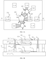
- FIG. 1A is a schematic top view of a semiconductor structure according to an exemplary embodiment of the present disclosure.
- in represents input
- out represents output
- Gnd represents ground.
- there are three input and three output which respectively correspond to the input and output of the first acoustic component, the second acoustic component and the third acoustic component, and two grounded of the third acoustic component.
- FIG. 1B is a schematic sectional view along a dashed line in FIG. 1A according to an exemplary embodiment of the present disclosure.
- a first unit and a second unit are sequentially stacked in a thickness direction of a semiconductor structure.
- the first unit includes a first substrate 10
- the second unit includes a second substrate 20, and an accommodating space is defined between the stacked first and second units.
- First acoustic component corresponding to reference signs 11, 12, and 13 are provided on an upper side of the first substrate 10.
- the second substrate 20 is a double-side functional substrate, and two sides of which are respectively provided with a second acoustic component corresponding to reference signs 212, 211A, and 213 and a third acoustic component corresponding to reference signs 222, 211B, and 223.
- FIG. 1B It can be seen from FIG. 1B that, three acoustic components are provided with respect to the two substrates, such that the number of substrates is less than the number of acoustic components.
- the acoustic component on the outermost side may be protected by film packaging during subsequent chip-level packaging, or may be further packaged by a capping layer substrate similar to that shown in FIG. 7 , which are all within the scope of the present disclosure.
- bulk acoustic wave resonators are arranged on two sides of the second substrate 20, which is used as the two-side functional substrate.
- the present disclosure is not limited thereto, for example, the two sides of the double-side functional substrate are respectively provided with a surface acoustic wave component, or the two sides of the double-side functional substrate are respectively provided with a surface acoustic wave component and a bulk acoustic wave component.
- the upper side of the second substrate 20 may be provided with an air cavity used as an acoustic mirror of the bulk acoustic wave resonator, and the lower side of the second substrate 20 may be provided with the surface acoustic wave resonator instead of the air cavity.
- air cavities 11, 211A and 211B used as cavities are acoustic mirrors of corresponding acoustic components.
- the acoustic mirror is not limited to the air cavity, and may be a Bragg reflection layer or other equivalent structure. Although not shown, the Bragg reflection layer may be arranged in the air cavity or arranged on the surface of the substrate.
- the air cavities on the upper and lower sides of the second substrate 20 are opposite to each other.
- a thickness of a portion of the substrate between the cavities on the two sides of the second substrate is not less than 20 ⁇ m.
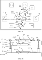
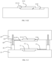
- FIG. 2A is a schematic top view of a semiconductor structure according to another exemplary embodiment of the present disclosure
- FIG. 2B is a schematic sectional view along a dashed line in FIG. 2A according to another exemplary embodiment of the present disclosure.
- the structure shown in FIG. 2B differs from the structure shown in FIG. 1B in that a releasing hole 60 for communicating the air cavities on the two sides of the second substrate 20 is provided in FIG. 2B , such that the two air cavities communicate with each other.
- 601 and 602 correspond to two forms of the releasing hole 60, which are both arranged within an effective region of the resonator, and of which cross-sectional shapes may be a circle, a square, or other shapes.
- the air cavity 211A on the lower side of the second substrate 20 needs to be formed firstly, and the air cavity 211B is then formed on the upper side of the second substrate 20.
- the two air cavities in FIG. 1B are formed separately, or the air cavity on the lower side is formed before the upper side of the second substrate is thinned.
- the air cavity on the upper side is formed after the thinning operation.
- the air cavities on the upper and lower sides of the second substrate communicate with each other through the releasing hole 60, such that a releasing channel that communicates with the air cavity on the upper side of the second substrate can releasing a sacrificial layer material in the air cavity located on the upper side and a sacrificial layer material in the air cavity located on the lower side.
- the sacrificial layer material in the air cavity located on the lower side functions to reinforce the second substrate since it is not removed. Since the firmness of the second substrate is enhanced, the thickness of the second substrate 20 can be further reduced, such that the space volume occupied by the semiconductor structure can be reduced.
- the thickness of the second substrate having the cavities on the two sides thereof includes depths of the air cavities on the upper side and the lower side, and is in a range of 6 ⁇ m to 50 ⁇ m.
- the thickness of the portion of the second substrate between the cavities located on the two sides of the second substrate is not less than 5 ⁇ m.
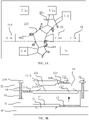
- FIG. 3A is a schematic top view of a semiconductor structure according to yet another exemplary embodiment of the present disclosure
- FIG. 3B is a schematic sectional view along a dashed line in FIG. 3A according to yet another exemplary embodiment of the present disclosure.
- FIG. 3B differs from FIG. 2B in that the releasing hole 60 is formed outside the effective region of the resonator in FIG. 3B .
- the releasing hole 60 is formed at the position of the releasing channel 225.
- FIG. 3C is a bottom view as viewed in a direction of an arrow in FIG. 3B . As shown in FIG. 3C , there is no releasing hole or releasing channel for releasing the sacrificial layer material in the air cavity 211A on the bulk acoustic wave resonators on the lower side and the lower side of the second substrate.
- 601 and 602 correspond to two forms of the releasing hole 60 that are both arranged outside the effective region of the resonator, and the cross-sectional shapes thereof may be a circle, a square, or other shapes.
- the sacrificial layer materials in the air cavities located on the upper and lower sides of the second substrate are simultaneously released from the releasing channel 225.
- the structure of FIG. 3B can achieve the same technical effects as the structure of FIG. 2B .
- the thickness of the second substrate used as a double-side functional substrate may be in the range of 6 ⁇ m to 50 ⁇ m.
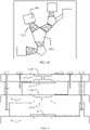
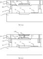
- FIG. 4 is a schematic sectional view along a dashed line similar to that of FIG. 1A according to yet another exemplary embodiment of the present disclosure.
- a third unit is provided in FIG. 4 .
- the third unit is an uppermost unit stacked on the upper side of the second unit, in which the second unit is arranged at the middle of the units.
- the third unit includes a third substrate 80 and two acoustic components located on the upper and lower sides of the third substrate, for example, filters.
- FIG. 4 is a schematic sectional view along a dashed line similar to that of FIG. 1A according to yet another exemplary embodiment of the present disclosure.
- the third unit is an uppermost unit stacked on the upper side of the second unit, in which the second unit is arranged at the middle of the units.
- the third unit includes a third substrate 80 and two acoustic components located on the upper and lower sides of the third substrate, for example, filters.
- the filter is a bulk acoustic wave filter.
- the number of substrates is increased, thereby increasing the number of acoustic components.
- three substrates are used to integrate five filters in FIG. 4 .
- FIG. 4 In the embodiment of FIG. 4 , three stacked substrates are shown, but more stacked substrates may be provided.
- the acoustic components are only arranged on the upper side of the substrate of the lowermost unit, and each of the other substrates is a double-side functional substrate. If all acoustic components arranged on one side of each substrate are collectively referred to as an integrated acoustic component that may include only one acoustic device, 2N-1 acoustic components can be integrated by using N (N is a natural number greater than 1) substrates, thereby greatly reducing the number of substrates and further reducing the volume of the entire semiconductor structure.
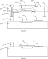
- FIG. 1B The manufacturing process of the structure of FIG. 1B is illustrated below with reference to FIG. 5-1 , FIGS. 5-2Ato 5-2C , and FIGS. 5-3 to 5-6 .
- Step 1 is to manufacture a first unit, as shown in FIG. 5-1 .
- a first acoustic component such as an FBAR component
- a first acoustic component of the bulk acoustic wave resonator include a bottom electrode, a piezoelectric layer, a top electrode, a cavity 11, and an external lead or electrode lead 13.
- a first metal bonding layer 30 is formed. In the illustration of the manufacturing process of the present disclosure, the manufacturing of the sealing layer 70 is not shown.
- Step 2 is to manufacture a second unit, as show in FIGS. 5-2A to 5-2C .
- a second acoustic component is formed on the second substrate 20.
- an external lead hole 50 is formed in FIG. 5-2B , and the hole 50 is formed in a metal bonding layer 40 and extends into a part of the second substrate 20.
- FIG. 5-2A is a partial top view of the second unit that is provided with the second acoustic component
- FIG. 5-2B is a sectional view along line A1-A2 in FIG. 5-2A
- FIG. 5-2C is a sectional view along line B1-B2 in FIG. 5-2A .
- the air cavity 211A is formed by injecting a solution (e.g., hydrofluoric acid) through the releasing channel 215 for the sacrificial layer material and releasing a reaction product.
- a solution e.g., hydrofluoric acid
- step 3 is to place the second substrate 20 upside down on the first substrate 10, and perform a bonding connection through the first metal bonding structure 30 and the second metal bonding structure 40.
- step 4 is to thin the second substrate 20 from the back surface.
- the second substrate is thinned by a CMP (chemical mechanical polishing) method until the hole 50 is exposed, so that the hole 50 is a conductive through hole.
- CMP chemical mechanical polishing
- the thinned thickness needs to be controlled.
- the depth of the air cavity 21 1A of the second substrate 20 is in a range of 0.5 ⁇ m to 10 ⁇ m, and is assumed to be 3 ⁇ m in an embodiment. In this way, the thickness of the thinned second substrate 20 should be controlled to be 3 ⁇ m +20 ⁇ m or more to prevent or reduce the risk of cracking and avoid influence on the process yield.
- step 5 is to form a third acoustic component, such as an FBAR component, on the back surface of the second substrate 20, in which the standard FBAR process may be utilized and thus no repeated description will be given herein.
- a third acoustic component such as an FBAR component
- step 6 is to form external electrical lead pads 14, 214, and 224 of the first acoustic component, the second acoustic component, and the third acoustic component on the back surface of the second substrate 20.
- the external leads of the first acoustic component and the second acoustic component are provided on a plane where the third acoustic component is located except for its own components and external leads.
- the area of the third acoustic component is smaller than those of the first acoustic component and the second acoustic component.
- the frequency of the third acoustic component is higher than those of the first acoustic component and the second acoustic component.
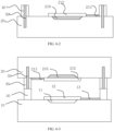
- FIG. 2B The manufacturing process of the structure of FIG. 2B is illustrated below with reference to FIGS. 6-1 to 6-7 .
- step 1 is to manufacture a first unit.
- a first acoustic component such as an FBAR component
- a first substrate 10 in which the standard FBAR process may be utilized and thus no repeated description will be given herein.
- acoustic components of the bulk acoustic wave resonator include a bottom electrode, a piezoelectric layer, a top electrode, a cavity 11, and an external lead or electrode lead 13.
- a first metal bonding layer 30 is formed. In the illustration of the manufacturing process of the present disclosure, the manufacturing of the sealing layer 70 is not shown.
- step 2 is to manufacture a second unit, and a second acoustic component is formed on the second substrate 20.
- external lead holes 50 are formed in FIG. 6-2 , and the holes 50 are formed in a metal bonding layer 40 and extend into a part of the second substrate 20.
- a sacrificial layer 216 is not released in FIG. 6-2 to function to reinforce the second substrate 20 during a subsequent thinning process.
- step 3 is to place the second substrate 20 upside down on the first substrate 10, and to perform a bonding connection through the first metal bonding structure 30 and the second metal bonding structure 40.
- step 4 is to thin the second substrate 20 from the back surface.
- the second substrate is thinned by the CMP (chemical mechanical polishing) method until the holes 50 are exposed, so that the holes 50 are conductive through holes.
- CMP chemical mechanical polishing
- the firmness of the second substrate 20 is improved, and therefore the thickness of the second substrate can be further reduced compared with the structure in FIG. 1B .
- the depth of the air cavity 211A formed on the front surface of the second substrate is in the range of 0.5 ⁇ m to 10 ⁇ m, and is assumed to be 3 ⁇ m.
- phosphor silicate glass is used as a sacrificial layer material, and has a density of about 2.2 g/cm 3 , which is substantially equivalent to that of a silicon substrate since the density of silicon is about 2.3 g/cm 3 .
- Borosilicate glass, boro-phosphor silicate glass and silicon dioxide all have similar properties. Accordingly, the thickness of the thinned second substrate should be controlled to be 3 ⁇ m+5 ⁇ m or more. If polyimide with a lower density is used as the sacrificial layer material, the density thereof is about 1.4 g/cm 3 .
- the mechanical strength of polyimide is poor, such that the thickness of the thinned second substrate 20 should be controlled to be 3 ⁇ m +10 ⁇ m or more.
- the density of the sacrificial material filled in the lower cavity is 80% or more of the density of the substrate, and the thickness of the thinned second substrate is in the range of 6 ⁇ m to 50 ⁇ m.
- the thickness of the thinned second substrate is in a range of 11 ⁇ m to 50 ⁇ m.
- step 5 is to form a sacrificial layer 216 and a sacrificial layer connection hole 60 of the third acoustic component.
- the sacrificial layer connection hole 60 is used to remove the sacrificial layer 216 when the sacrificial layer 216 is subsequently removed, to complete the manufacturing of the air cavities of the second acoustic component and the third acoustic component.
- a diameter of the sacrificial layer connection hole 60 is selected to range from 0.5 ⁇ m to 20 ⁇ m, to prevent photoresist from flowing into the connection hole 60 during a subsequent photoresist coating process.
- step 6 is to form a subsequent structure of the third acoustic component. While the sacrificial layer 216 of the third acoustic component is removed to form the air cavity 211B, the sacrificial layer 216 of the second acoustic component is removed to form the air cavity 211A.
- step 7 is to form external electrical lead pads 14, 214, and 224 of the first acoustic component, the second acoustic component, and the third acoustic component on the back surface of the second substrate 20.
- the external leads of the first acoustic component and the second acoustic component are provided on a plane where the third acoustic component is located except for its own components and external leads.
- the area of the third acoustic component is smaller than those of the first acoustic component and the second acoustic component.
- the acoustic component (filter) with the highest frequency that has the minimum area is arranged on the upper surface of the second unit as the third acoustic component.
- the manufacturing process of the semiconductor structure shown in FIG. 3B is similar to the manufacturing process of FIG. 2B , except that during the manufacturing process of the structure shown in FIG. 3B , when the second acoustic component is formed on the front surface of the second substrate, the air cavity 211A that is correspondingly filled with the sacrificial layer material extends to the lower side of the releasing channel located on the back surface of the second substrate. Other components of the second acoustic component completely cover the air cavity 211A.
- the manufacturing process of the structure shown in FIG. 4 is similar to that of FIG. 2B , and the step of processing the second substrate 20 is repeated on the third substrate 80, i.e., step 2 to step 6. Step 7 is finally performed to form the external lead.
- upper and lower are described based on the bottom surface of the substrate (of which one side is not provided with an acoustic component) on the lowermost side of the unit, which is only provided with the acoustic component on a single side.
- a side of the other components closer to the bottom surface is the lower side, and the side further away from the bottom surface is the upper side.
- the electronic device herein may include, but is not limited to, intermediate products such as a radio-frequency front end, and a filtering and amplifying module, and terminal products such as a mobile phone, WIFI and an unmanned aerial vehicle.
Landscapes
- Physics & Mathematics (AREA)
- Acoustics & Sound (AREA)
- Engineering & Computer Science (AREA)
- Manufacturing & Machinery (AREA)
- Piezo-Electric Or Mechanical Vibrators, Or Delay Or Filter Circuits (AREA)
Applications Claiming Priority (2)
| Application Number | Priority Date | Filing Date | Title |
|---|---|---|---|
| CN202010358033.9A CN111883645B (zh) | 2020-04-29 | 2020-04-29 | 具有叠置单元的半导体结构及制造方法、电子设备 |
| PCT/CN2021/090819 WO2021219051A1 (zh) | 2020-04-29 | 2021-04-29 | 具有叠置单元的半导体结构及制造方法、电子设备 |
Publications (2)
| Publication Number | Publication Date |
|---|---|
| EP4145545A1 true EP4145545A1 (de) | 2023-03-08 |
| EP4145545A4 EP4145545A4 (de) | 2023-11-01 |
Family
ID=73153981
Family Applications (1)
| Application Number | Title | Priority Date | Filing Date |
|---|---|---|---|
| EP21796977.3A Pending EP4145545A4 (de) | 2020-04-29 | 2021-04-29 | Halbleiterstruktur mit gestapelten einheiten und herstellungsverfahren dafür sowie elektronische vorrichtung |
Country Status (3)
| Country | Link |
|---|---|
| EP (1) | EP4145545A4 (de) |
| CN (1) | CN111883645B (de) |
| WO (1) | WO2021219051A1 (de) |
Families Citing this family (2)
| Publication number | Priority date | Publication date | Assignee | Title |
|---|---|---|---|---|
| CN111883645B (zh) * | 2020-04-29 | 2021-09-21 | 诺思(天津)微系统有限责任公司 | 具有叠置单元的半导体结构及制造方法、电子设备 |
| CN116032246B (zh) * | 2023-03-27 | 2023-10-31 | 成都频岢微电子有限公司 | 一种双工器 |
Family Cites Families (10)
| Publication number | Priority date | Publication date | Assignee | Title |
|---|---|---|---|---|
| US6808954B2 (en) * | 2001-09-07 | 2004-10-26 | Intel Corporation | Vacuum-cavity MEMS resonator |
| KR100622955B1 (ko) * | 2004-04-06 | 2006-09-18 | 삼성전자주식회사 | 박막 벌크 음향 공진기 및 그 제조방법 |
| JP4375399B2 (ja) * | 2004-07-20 | 2009-12-02 | 株式会社村田製作所 | 圧電フィルタ |
| CN203503623U (zh) * | 2013-10-21 | 2014-03-26 | 安徽北方芯动联科微系统技术有限公司 | 基于导电柱圆片级封装的单片集成式mems芯片 |
| CN103873010B (zh) * | 2014-03-17 | 2017-03-22 | 电子科技大学 | 一种压电薄膜体声波谐振器及其制备方法 |
| US10110189B2 (en) * | 2016-11-02 | 2018-10-23 | Akoustis, Inc. | Structure and method of manufacture for acoustic resonator or filter devices using improved fabrication conditions and perimeter structure modifications |
| WO2019132921A1 (en) * | 2017-12-28 | 2019-07-04 | Intel Corporation | Hybrid filter architecture with integrated passives, acoustic wave resonators and hermetically sealed cavities between two resonator dies |
| CN108667437B (zh) * | 2018-04-19 | 2022-04-26 | 中芯集成电路(宁波)有限公司 | 一种薄膜体声波谐振器及其制造方法和电子装置 |
| CN111049489B (zh) * | 2019-12-31 | 2021-06-01 | 诺思(天津)微系统有限责任公司 | 具有叠置单元的半导体结构及制造方法、电子设备 |
| CN111883645B (zh) * | 2020-04-29 | 2021-09-21 | 诺思(天津)微系统有限责任公司 | 具有叠置单元的半导体结构及制造方法、电子设备 |
-
2020
- 2020-04-29 CN CN202010358033.9A patent/CN111883645B/zh active Active
-
2021
- 2021-04-29 WO PCT/CN2021/090819 patent/WO2021219051A1/zh not_active Ceased
- 2021-04-29 EP EP21796977.3A patent/EP4145545A4/de active Pending
Also Published As
| Publication number | Publication date |
|---|---|
| CN111883645B (zh) | 2021-09-21 |
| EP4145545A4 (de) | 2023-11-01 |
| WO2021219051A1 (zh) | 2021-11-04 |
| CN111883645A (zh) | 2020-11-03 |
Similar Documents
| Publication | Publication Date | Title |
|---|---|---|
| CN112039472B (zh) | 一种薄膜声波滤波器及其制造方法 | |
| CN112039466B (zh) | 一种薄膜体声波谐振器及其制造方法 | |
| CN110401428B (zh) | 薄膜体声波谐振器及其制造方法 | |
| US7579926B2 (en) | FBAR band pass filter, duplexer having the filter and methods for manufacturing the same | |
| CN110719082B (zh) | 声波谐振器封装件 | |
| CN111049489B (zh) | 具有叠置单元的半导体结构及制造方法、电子设备 | |
| WO2019029912A1 (en) | BAW RESONATOR WITH REDUCED PARASITE MODES AND ENHANCED QUALITY FACTOR | |
| CN108631748B (zh) | 声波谐振器及包括该声波谐振器的滤波器 | |
| US12506458B2 (en) | Packaging module and packaging method of BAW resonator | |
| US12603639B2 (en) | Metal cavity for transversely-excited film bulk acoustic resonator (XBAR) | |
| CN114684778A (zh) | 一种mems器件及其制作方法 | |
| CN112087216B (zh) | 具有声学孔的体声波谐振器及组件、滤波器及电子设备 | |
| CN112787614A (zh) | 一种薄膜拉姆波谐振器、滤波器及其制造方法 | |
| CN111130493B (zh) | 具有叠置单元的半导体结构及制造方法、电子设备 | |
| CN111030627A (zh) | 声波器件的制作方法及声波器件 | |
| CN114793102B (zh) | 体声波谐振器组、制备方法及体声波滤波器、通信器件 | |
| US20230041856A1 (en) | Transversely-excited film bulk acoustic resonator (xbar) | |
| EP4145545A1 (de) | Halbleiterstruktur mit gestapelten einheiten und herstellungsverfahren dafür sowie elektronische vorrichtung | |
| CN115001434B (zh) | 具有分叉电极的膜体声学谐振器 | |
| CN113054941B (zh) | 声波谐振器制作方法及声波谐振器 | |
| US20220399874A1 (en) | Acoustic wave resonator package | |
| CN116436425A (zh) | 体声波滤波器的制造方法、体声波滤波器、多工器及射频模组 | |
| CN114070255A (zh) | 叠置体声波谐振器组件及制造方法、滤波器及电子设备 | |
| US20260113012A1 (en) | Acoustic wave device with enhanced quality factor and fabrication method thereof | |
| US20240195384A1 (en) | Multiple membrane thickness wafers using layer transfer acoustic resonators and method of manufacturing same |
Legal Events
| Date | Code | Title | Description |
|---|---|---|---|
| STAA | Information on the status of an ep patent application or granted ep patent |
Free format text: STATUS: THE INTERNATIONAL PUBLICATION HAS BEEN MADE |
|
| PUAI | Public reference made under article 153(3) epc to a published international application that has entered the european phase |
Free format text: ORIGINAL CODE: 0009012 |
|
| STAA | Information on the status of an ep patent application or granted ep patent |
Free format text: STATUS: REQUEST FOR EXAMINATION WAS MADE |
|
| 17P | Request for examination filed |
Effective date: 20221129 |
|
| AK | Designated contracting states |
Kind code of ref document: A1 Designated state(s): AL AT BE BG CH CY CZ DE DK EE ES FI FR GB GR HR HU IE IS IT LI LT LU LV MC MK MT NL NO PL PT RO RS SE SI SK SM TR |
|
| DAV | Request for validation of the european patent (deleted) | ||
| DAX | Request for extension of the european patent (deleted) | ||
| REG | Reference to a national code |
Ref country code: DE Ref legal event code: R079 Free format text: PREVIOUS MAIN CLASS: H01L0041053000 Ipc: H03H0009100000 |
|
| A4 | Supplementary search report drawn up and despatched |
Effective date: 20230929 |
|
| RIC1 | Information provided on ipc code assigned before grant |
Ipc: H03H 3/02 20060101ALI20230925BHEP Ipc: H03H 9/05 20060101ALI20230925BHEP Ipc: H03H 3/007 20060101ALI20230925BHEP Ipc: H03H 9/10 20060101AFI20230925BHEP |