EP4148478B1 - Ensemble système d'imagerie optique, appareil d'imagerie et dispositif électronique - Google Patents
Ensemble système d'imagerie optique, appareil d'imagerie et dispositif électronique Download PDFInfo
- Publication number
- EP4148478B1 EP4148478B1 EP22177853.3A EP22177853A EP4148478B1 EP 4148478 B1 EP4148478 B1 EP 4148478B1 EP 22177853 A EP22177853 A EP 22177853A EP 4148478 B1 EP4148478 B1 EP 4148478B1
- Authority
- EP
- European Patent Office
- Prior art keywords
- lens element
- image
- imaging system
- system assembly
- lens
- Prior art date
- Legal status (The legal status is an assumption and is not a legal conclusion. Google has not performed a legal analysis and makes no representation as to the accuracy of the status listed.)
- Active
Links
Images










Classifications
-
- G—PHYSICS
- G02—OPTICS
- G02B—OPTICAL ELEMENTS, SYSTEMS OR APPARATUS
- G02B13/00—Optical objectives specially designed for the purposes specified below
- G02B13/001—Miniaturised objectives for electronic devices, e.g. portable telephones, webcams, PDAs, small digital cameras
- G02B13/0015—Miniaturised objectives for electronic devices, e.g. portable telephones, webcams, PDAs, small digital cameras characterised by the lens design
- G02B13/002—Miniaturised objectives for electronic devices, e.g. portable telephones, webcams, PDAs, small digital cameras characterised by the lens design having at least one aspherical surface
- G02B13/0045—Miniaturised objectives for electronic devices, e.g. portable telephones, webcams, PDAs, small digital cameras characterised by the lens design having at least one aspherical surface having five or more lenses
-
- G—PHYSICS
- G02—OPTICS
- G02B—OPTICAL ELEMENTS, SYSTEMS OR APPARATUS
- G02B13/00—Optical objectives specially designed for the purposes specified below
- G02B13/18—Optical objectives specially designed for the purposes specified below with lenses having one or more non-spherical faces, e.g. for reducing geometrical aberration
-
- G—PHYSICS
- G02—OPTICS
- G02B—OPTICAL ELEMENTS, SYSTEMS OR APPARATUS
- G02B9/00—Optical objectives characterised both by the number of the components and their arrangements according to their sign, i.e. + or -
- G02B9/64—Optical objectives characterised both by the number of the components and their arrangements according to their sign, i.e. + or - having more than six components
Definitions
- the present disclosure relates to an optical imaging system assembly and an imaging apparatus. More particularly, the present disclosure relates to an optical imaging system assembly and an imaging apparatus with compact size applicable to electronic devices.
- the reference US 2019/0154974 A1 discloses an optical imaging lens assembly including seven lens elements, and the seventh lens element has an image-side surface being concave in a paraxial region thereof.
- the reference US 2016/0241756 A1 discloses a photographing system including seven lens elements. The first lens element with positive refractive power has an object-side surface being convex in a paraxial region thereof.
- the second lens element with refractive power has an image-side surface being concave in a paraxial region thereof.
- the sixth lens element with refractive power has an image-surface being concave in a paraxial region thereof.
- the seventh lens element with refractive power has an object-side surface being concave in a paraxial region thereof.
- the reference CN 112748535 A discloses an optical lens including seven lens elements. However, in a conventional optical lens assembly, it is hard to balance among image quality, sensitivity, aperture size, volume or field of view. Thus, there is a demand for an optical imaging system assembly that meets the aforementioned needs.
- an optical imaging system assembly includes seven lens elements, the seven lens elements being, in order from an object side to an image side along an optical path, a first lens element, a second lens element, a third lens element, a fourth lens element, a fifth lens element, a sixth lens element and a seventh lens element.
- Each of the seven lens elements has an object-side surface towards the object side and an image-side surface towards the image side.
- the first lens element has positive refractive power.
- the object-side surface of the first lens element is convex in a paraxial region thereof, the image-side surface of the first lens element is concave in a paraxial region thereof.
- the second lens element has negative refractive power.
- the object-side surface of the third lens element is convex in a paraxial region thereof.
- the fifth lens element has positive refractive power.
- the sixth lens element has negative refractive power.
- the seventh lens element has negative refractive power. At least one of the object-side surface and the image-side surface of at least one of the first lens element to the seventh lens element includes at least one inflection point.
- an Abbe number of the fourth lens element is V4
- an Abbe number of the fifth lens element is V5
- an Abbe number of the sixth lens element is V6
- a central thickness of the first lens element is CT1
- a central thickness of the second lens element is CT2
- a central thickness of the third lens element is CT3
- a central thickness of the fourth lens element is CT4
- a central thickness of the fifth lens element is CT5
- a central thickness of the sixth lens element is CT6
- an axial distance between the sixth lens element and the seventh lens element is T67
- an f-number of the optical imaging system assembly is Fno
- half of a maximum field of view of the optical imaging system assembly is HFOV
- a focal length of the optical imaging system assembly is f
- a focal length of the third lens element is f3
- a focal length of the fourth lens element is f4
- a focal length of the seventh lens element is f7
- the Abbe number of the fourth lens element is V4
- the Abbe number of the fifth lens element is V5
- the Abbe number of the sixth lens element is V6
- the central thickness of the first lens element is CT1
- the central thickness of the second lens element is CT2
- the central thickness of the third lens element is CT3
- the central thickness of the fourth lens element is CT4
- the central thickness of the fifth lens element is CT5
- the central thickness of the sixth lens element is CT6
- the axial distance between the sixth lens element and the seventh lens element is T67
- the following conditions are satisfied: 4.9 ⁇ (V5+V6)N4 ⁇ 11; and 2.0 ⁇ (CT1+CT2+CT3+CT4+CT5+CT6)/T67 ⁇ 3.2.
- an electronic device includes the imaging apparatus of the aforementioned aspect.
- An optical imaging system assembly includes seven lens elements, the seven lens elements being, in order from an object side to an image side along an optical path, a first lens element, a second lens element, a third lens element, a fourth lens element, a fifth lens element, a sixth lens element and a seventh lens element.
- Each of the seven lens elements has an object-side surface towards the object side and an image-side surface towards the image side.
- the first lens element has positive refractive power, which is favorable for compressing the volume of the object side of the optical imaging system assembly.
- the object-side surface of the first lens element is convex in a paraxial region thereof, so that the direction of the light entering into the optical imaging system assembly can be adjusted so as to enlarge field of view.
- the image-side surface of the first lens element is concave in a paraxial region thereof, so that it is favorable for correcting aberrations, such as astigmatism etc., by adjusting the surface shape of the first lens element.
- the object-side surface of the third lens element is convex in a paraxial region thereof, so that it is favorable for correcting aberrations, such as spherical aberrations etc., by adjusting the surface shape of the third lens element.
- the fifth lens element has positive refractive power, which is favorable for compressing the volume of the image side of the optical imaging system assembly.
- the object-side surface of the fifth lens element can be concave in a paraxial region thereof, so that it is favorable for balancing the volume arrangement of the optical imaging system assembly by adjusting the traveling direction of the light.
- the image-side surface of the fifth lens element can be convex in a paraxial region thereof, so that it is favorable for enlarging the image surface by adjusting the traveling direction of the light.
- the sixth lens element has negative refractive power, which can be cooperated with the fifth lens element so as to correct aberrations.
- the object-side surface of the sixth lens element can be convex in a paraxial region thereof, so that it is favorable for correcting aberrations by adjusting the surface shape of the sixth lens element.
- the image-side surface of the sixth lens element can be concave in a paraxial region thereof, which can be cooperated with the seventh lens element so as to correct aberrations.
- the seventh lens element has negative refractive power, so that it is favorable for correcting aberrations by balancing the refractive power of the image side of the optical imaging system assembly.
- the object-side surface of the seventh lens element can be concave in a paraxial region thereof, so that it is favorable for enlarging the image surface by adjusting the traveling direction of the light.
- the image-side surface of the seventh lens element can be concave in a paraxial region thereof, so that it is favorable for reducing the back focal length.
- At least one of the object-side surface and the image-side surface of at least one of the first lens element to the seventh lens element includes at least one inflection point. Therefore, it is favorable for correcting aberrations and compressing the size of the lens elements by increasing the variation of the surfaces of the lens elements. Further, at least one of the object-side surface and the image-side surface of each of at least two of the first lens element to the seventh lens element can include at least one inflection point. Furthermore, at least one of the object-side surface and the image-side surface of each of at least three of the first lens element to the seventh lens element can include at least one inflection point.
- the object-side surface of the sixth lens element can have at least one critical point in an off-axis region thereof, so that it is favorable for reducing the surface reflection and correcting off-axis aberrations by adjusting the surface shape of the sixth lens element.
- a distance between the at least one critical point of the object-side surface of the sixth lens element and an optical axis is Yc61
- a maximum distance between an optical effective region of the object-side surface of the sixth lens element and the optical axis is Y61
- the surface shape of the sixth lens element can be further adjusted so as to correct aberrations.
- the image-side surface of the sixth lens element can have at least one critical point in an off-axis region thereof, so that it is favorable for correcting off-axis aberrations, such as field curvature etc., by adjusting the surface shape of the sixth lens element.
- a distance between the at least one critical point of the image-side surface of the sixth lens element and the optical axis is Yc62
- a maximum distance between an optical effective region of the image-side surface of the sixth lens element and the optical axis is Y62
- the surface shape of the sixth lens element can be further adjusted so as to correct aberrations.
- the image-side surface of the seventh lens element can have at least one critical point in an off-axis region thereof, so that it is favorable for enhancing the image quality and the response efficiency of the image sensor by adjusting the incident angle of the light on the image surface.
- a distance between the at least one critical point of the image-side surface of the seventh lens element and the optical axis is Yc72
- a maximum distance between an optical effective region of the image-side surface of the seventh lens element and the optical axis is Y72
- an Abbe number of the fourth lens element is V4
- an Abbe number of the fifth lens element is V5
- an Abbe number of the sixth lens element is V6
- the following condition is satisfied: 4.4 ⁇ (V5+V6)/V4 ⁇ 12. Therefore, it is favorable for correcting aberrations, such as chromatic aberrations etc., by cooperating the material of the lens elements. Further, the following condition can be satisfied: 4.9 ⁇ (V5+V6)N4 ⁇ 11. Furthermore, the following condition can be satisfied: 5.3 ⁇ (V5+V6)N4 ⁇ 10. Moreover, the following condition can be satisfied: 5.7 ⁇ (V5+V6)N4 ⁇ 9.0.
- the following condition is satisfied: 2.1 ⁇ T67/T23 ⁇ 5.4. Therefore, it is favorable for compressing the volume of the optical imaging system assembly by adjusting the lens element arrangement thereof. Further, the following condition can be satisfied: 2.4 ⁇ T671T23 ⁇ 4.8. Furthermore, the following condition can be satisfied: 2.7 ⁇ T67/T23 ⁇ 4.3.
- a central thickness of the first lens element is CT1
- a central thickness of the second lens element is CT2
- a central thickness of the third lens element is CT3
- a central thickness of the fourth lens element is CT4
- a central thickness of the fifth lens element is CT5
- a central thickness of the sixth lens element is CT6, and the axial distance between the sixth lens element and the seventh lens element is T67
- the following condition is satisfied: 1.0 ⁇ (CT1+CT2+CT3+CT4+CT5+CT6)/T67 ⁇ 3.5. Therefore, it is favorable for compressing the volume of the optical imaging system assembly by adjusting the lens element arrangement thereof. Further, the following condition can be satisfied: 2.0 ⁇ (CT1+CT2+CT3+CT4+CT5+CT6)/T67 ⁇ 3.2.
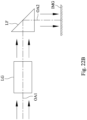
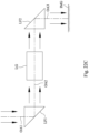
- the optical imaging system assembly includes, in order from an imaged object (not shown in drawings) to an image surface IMG, a first optical axis OA1, the light path folding element LF and a second optical axis OA2, wherein the light path folding element LF can be disposed between the imaged object and a lens group LG of the optical imaging system assembly as shown in Fig. 22A , or can be disposed between the lens group LG of the optical imaging system assembly and the image surface IMG as shown in Fig. 22B .
- Fig. 22C is a schematic view of an arrangement of two light path folding elements LF1, LF2 in the optical imaging system assembly of the present disclosure. As shown in Fig.
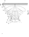
- the sixth lens element E6 with negative refractive power has an object-side surface being convex in a paraxial region thereof and an image-side surface being concave in a paraxial region thereof.
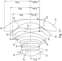
- the sixth lens element E6 is made of a plastic material, and has the object-side surface and the image-side surface being both aspheric. Furthermore, the object-side surface of the sixth lens element E6 includes two inflection points IP (as shown in Fig. 17 ) and one critical point CP (as shown in Fig. 17 ) in an off-axis region thereof, and the image-side surface of the sixth lens element E6 includes two inflection points IP (as shown in Fig. 17 ) and one critical point CP (as shown in Fig. 17 ) in an off-axis region thereof.
- the seventh lens element E7 with negative refractive power has an object-side surface being concave in a paraxial region thereof and an image-side surface being concave in a paraxial region thereof.
- the seventh lens element E7 is made of a plastic material, and has the object-side surface and the image-side surface being both aspheric. Furthermore, the object-side surface of the seventh lens element E7 includes one inflection point IP (as shown in Fig. 17 ), and the image-side surface of the seventh lens element E7 includes two inflection points IP (as shown in Fig. 17 ) and one critical point CP (as shown in Fig. 17 ) in an off-axis region thereof.
- a central thickness of the first lens element E1 is CT1
- a central thickness of the second lens element E2 is CT2
- a central thickness of the third lens element E3 is CT3
- a central thickness of the fourth lens element E4 is CT4
- a central thickness of the fifth lens element E5 is CT5
- a central thickness of the sixth lens element E6 is CT6
- an axial distance between the first lens element E1 and the second lens element E2 is T12
- an axial distance between the second lens element E2 and the third lens element E3 is T23
- an axial distance between the sixth lens element E6 and the seventh lens element E7 is T67
- an entrance pupil diameter of the optical imaging system assembly is EPD
- the focal length of the optical imaging system assembly is f
- a maximum image height of the optical imaging system assembly is ImgH
- a curvature radius of the object-side surface of the sixth lens element E6 is R11
- a curvature radius of the image-side surface of the sixth lens element E6 is R12
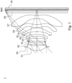
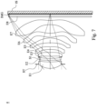
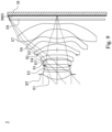
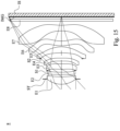
- Fig. 3 is a schematic view of an imaging apparatus 2 according to the 2nd embodiment of the present disclosure.
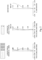
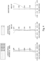
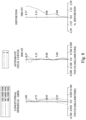
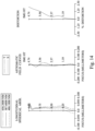
- Fig. 4 shows spherical aberration curves, astigmatic field curves and a distortion curve of the imaging apparatus 2 according to the 2nd embodiment.
- the imaging apparatus 2 includes an optical imaging system assembly (its reference numeral is omitted) and an image sensor IS.
- the first lens element E1 with positive refractive power has an object-side surface being convex in a paraxial region thereof and an image-side surface being concave in a paraxial region thereof.
- the first lens element E1 is made of a plastic material, and has the object-side surface and the image-side surface being both aspheric. Furthermore, the object-side surface of the first lens element E1 includes one inflection point, and the image-side surface of the first lens element E1 includes one inflection point.
- the fourth lens element E4 with negative refractive power has an object-side surface being concave in a paraxial region thereof and an image-side surface being convex in a paraxial region thereof.
- the fourth lens element E4 is made of a plastic material, and has the object-side surface and the image-side surface being both aspheric. Furthermore, the image-side surface of the fourth lens element E4 includes one inflection point.
- the fifth lens element E5 with positive refractive power has an object-side surface being concave in a paraxial region thereof and an image-side surface being convex in a paraxial region thereof.
- the fifth lens element E5 is made of a plastic material, and has the object-side surface and the image-side surface being both aspheric. Furthermore, the object-side surface of the fifth lens element E5 includes one inflection point, and the image-side surface of the fifth lens element E5 includes two inflection points.
- the filter E8 is made of a glass material, which is located between the seventh lens element E7 and the image surface IMG in order, and will not affect the focal length of the optical imaging system assembly.
- Table 3 The detailed optical data of the 2nd embodiment are shown in Table 3 and the aspheric surface data are shown in Table 4 below.
- Effective radius of Surface 6 (stop S1) is 1.290 mm. Effective radius of Surface 11 (stop S2) is 2.005 mm.
- Table 4 - Aspheric Coefficients Surface # 2 3 4 5 7 k 1.37277E-01 3.84522E+00 9.47611E+01 4.84260E+00 -8.51358E+01
- A4 1.234039231E-03 -2.104610909E-02 -6.449983813E-02 -5.765899626E-02 -2.974078130E-02
- A6 -6.473681636E-03 1.225595392E-02 8.270002855E-02 5.905345825E-02 -1.362555596E-02
- the equation of the aspheric surface profiles of the aforementioned lens elements is the same as the equation of the 1st embodiment. Also, the definitions of these parameters shown in the following table are the same as those stated in the 1st embodiment with corresponding values for the 2nd embodiment, so an explanation in this regard will not be provided again.
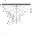
- Fig. 5 is a schematic view of an imaging apparatus 3 according to the 3rd embodiment of the present disclosure.
- Fig. 6 shows spherical aberration curves, astigmatic field curves and a distortion curve of the imaging apparatus 3 according to the 3rd embodiment.
- the imaging apparatus 3 includes an optical imaging system assembly (its reference numeral is omitted) and an image sensor IS.
- the optical imaging system assembly includes, in order from an object side to an image side along an optical path, an aperture stop ST, a first lens element E1, a second lens element E2, a stop S1, a third lens element E3, a fourth lens element E4, a stop S2, a fifth lens element E5, a sixth lens element E6, a seventh lens element E7, a filter E8 and an image surface IMG, wherein the image sensor IS is disposed on the image surface IMG of the optical imaging system assembly.
- the optical imaging system assembly includes seven lens elements (E1, E2, E3, E4, E5, E6, E7) without additional one or more lens elements inserted between the first lens element E1 and the seventh lens element E7.
- the first lens element E1 with positive refractive power has an object-side surface being convex in a paraxial region thereof and an image-side surface being concave in a paraxial region thereof.
- the first lens element E1 is made of a glass material, and has the object-side surface and the image-side surface being both aspheric. Furthermore, the image-side surface of the first lens element E1 includes one inflection point.
- the second lens element E2 with negative refractive power has an object-side surface being convex in a paraxial region thereof and an image-side surface being concave in a paraxial region thereof.
- the second lens element E2 is made of a plastic material, and has the object-side surface and the image-side surface being both aspheric. Furthermore, the object-side surface of the second lens element E2 includes two inflection points.
- the third lens element E3 with positive refractive power has an object-side surface being convex in a paraxial region thereof and an image-side surface being convex in a paraxial region thereof.
- the third lens element E3 is made of a plastic material, and has the object-side surface and the image-side surface being both aspheric. Furthermore, the object-side surface of the third lens element E3 includes one inflection point.
- the fourth lens element E4 with negative refractive power has an object-side surface being concave in a paraxial region thereof and an image-side surface being concave in a paraxial region thereof.
- the fourth lens element E4 is made of a plastic material, and has the object-side surface and the image-side surface being both aspheric. Furthermore, the image-side surface of the fourth lens element E4 includes two inflection points.
- the fifth lens element E5 with positive refractive power has an object-side surface being concave in a paraxial region thereof and an image-side surface being convex in a paraxial region thereof.
- the fifth lens element E5 is made of a plastic material, and has the object-side surface and the image-side surface being both aspheric. Furthermore, the object-side surface of the fifth lens element E5 includes one inflection point, and the image-side surface of the fifth lens element E5 includes two inflection points.
- the sixth lens element E6 with negative refractive power has an object-side surface being convex in a paraxial region thereof and an image-side surface being concave in a paraxial region thereof.
- the sixth lens element E6 is made of a plastic material, and has the object-side surface and the image-side surface being both aspheric. Furthermore, the object-side surface of the sixth lens element E6 includes two inflection points and one critical point in an off-axis region thereof, and the image-side surface of the sixth lens element E6 includes two inflection points and one critical point in an off-axis region thereof.
- the seventh lens element E7 with negative refractive power has an object-side surface being concave in a paraxial region thereof and an image-side surface being concave in a paraxial region thereof.
- the seventh lens element E7 is made of a plastic material, and has the object-side surface and the image-side surface being both aspheric. Furthermore, the object-side surface of the seventh lens element E7 includes one inflection point, and the image-side surface of the seventh lens element E7 includes two inflection points and one critical point in an off-axis region thereof.
- Table 5 The detailed optical data of the 3rd embodiment are shown in Table 5 and the aspheric surface data are shown in Table 6 below.
- the equation of the aspheric surface profiles of the aforementioned lens elements is the same as the equation of the 1st embodiment. Also, the definitions of these parameters shown in the following table are the same as those stated in the 1st embodiment with corresponding values for the 3rd embodiment, so an explanation in this regard will not be provided again.
- the optical imaging system assembly includes, in order from an object side to an image side along an optical path, an aperture stop ST, a first lens element E1, a second lens element E2, a stop S1, a third lens element E3, a fourth lens element E4, a fifth lens element E5, a sixth lens element E6, a seventh lens element E7, a filter E8 and an image surface IMG, wherein the image sensor IS is disposed on the image surface IMG of the optical imaging system assembly.
- the optical imaging system assembly includes seven lens elements (E1, E2, E3, E4, E5, E6, E7) without additional one or more lens elements inserted between the first lens element E1 and the seventh lens element E7.
- Effective radius of Surface 6 (stop S1) is 2.06 mm.
- A4 -2.168082465E-04 -3.763223132E-03 -1.418254226E-02 -1.472000880E-02 -7.581401865E-03
- A6 2.239675357E-04 2.215214259E-04 5.926003575E-03 7.312644566E-03 -1.694524157E-03
- A8 -1.269460556E-04 6.219427978E-04 -1.409847517E-03 -2.491672506E-03 1.599373746E-03
- A10 4.296367941E-05 -4.267013351 E-04 3.000800762E-04 8.558709957E-04
- the first lens element E1 with positive refractive power has an object-side surface being convex in a paraxial region thereof and an image-side surface being concave in a paraxial region thereof.
- the first lens element E1 is made of a plastic material, and has the object-side surface and the image-side surface being both aspheric. Furthermore, the object-side surface of the first lens element E1 includes one inflection point, and the image-side surface of the first lens element E1 includes one inflection point.
- the second lens element E2 with negative refractive power has an object-side surface being convex in a paraxial region thereof and an image-side surface being concave in a paraxial region thereof.
- the second lens element E2 is made of a plastic material, and has the object-side surface and the image-side surface being both aspheric. Furthermore, the object-side surface of the second lens element E2 includes two inflection points.
- the fourth lens element E4 with positive refractive power has an object-side surface being convex in a paraxial region thereof and an image-side surface being concave in a paraxial region thereof.
- the fourth lens element E4 is made of a plastic material, and has the object-side surface and the image-side surface being both aspheric. Furthermore, the object-side surface of the fourth lens element E4 includes one inflection point, and the image-side surface of the fourth lens element E4 includes two inflection points.
- the fifth lens element E5 with positive refractive power has an object-side surface being concave in a paraxial region thereof and an image-side surface being convex in a paraxial region thereof.
- the fifth lens element E5 is made of a plastic material, and has the object-side surface and the image-side surface being both aspheric. Furthermore, the object-side surface of the fifth lens element E5 includes two inflection points, and the image-side surface of the fifth lens element E5 includes two inflection points.
- the sixth lens element E6 with negative refractive power has an object-side surface being convex in a paraxial region thereof and an image-side surface being concave in a paraxial region thereof.
- the sixth lens element E6 is made of a plastic material, and has the object-side surface and the image-side surface being both aspheric. Furthermore, the object-side surface of the sixth lens element E6 includes two inflection points and one critical point in an off-axis region thereof, and the image-side surface of the sixth lens element E6 includes two inflection points and one critical point in an off-axis region thereof.
- the seventh lens element E7 with negative refractive power has an object-side surface being concave in a paraxial region thereof and an image-side surface being concave in a paraxial region thereof.
- the seventh lens element E7 is made of a plastic material, and has the object-side surface and the image-side surface being both aspheric. Furthermore, the object-side surface of the seventh lens element E7 includes one inflection point, and the image-side surface of the seventh lens element E7 includes one inflection point and one critical point in an off-axis region thereof.
- the filter E8 is made of a glass material, which is located between the seventh lens element E7 and the image surface IMG in order, and will not affect the focal length of the optical imaging system assembly.
- Table 9 The detailed optical data of the 5th embodiment are shown in Table 9 and the aspheric surface data are shown in Table 10 below.
- Effective radius of Surface 6 (stop S1) is 1.285 mm. Effective radius of Surface 11 (stop S2) is 2.000 mm.
- Table 10 - Aspheric Coefficients Surface # 2 3 4 5 7 k 3.88221E-02 -3.85864E+00 9.33827E+01 7.66443E+00 -8.92496E+01
- A4 -1.302602543E-03 -1.843688353E-02 -6.218797748E-02 -5.312952999E-02 -3.509645726E-02
- the equation of the aspheric surface profiles of the aforementioned lens elements is the same as the equation of the 1st embodiment. Also, the definitions of these parameters shown in the following table are the same as those stated in the 1st embodiment with corresponding values for the 5th embodiment, so an explanation in this regard will not be provided again.
- Fig. 11 is a schematic view of an imaging apparatus 6 according to the 6th embodiment of the present disclosure.
- Fig. 12 shows spherical aberration curves, astigmatic field curves and a distortion curve of the imaging apparatus 6 according to the 6th embodiment.
- the imaging apparatus 6 includes an optical imaging system assembly (its reference numeral is omitted) and an image sensor IS.
- the optical imaging system assembly includes, in order from an object side to an image side along an optical path, an aperture stop ST, a first lens element E1, a second lens element E2, a stop S1, a third lens element E3, a fourth lens element E4, a stop S2, a fifth lens element E5, a sixth lens element E6, a seventh lens element E7, a filter E8 and an image surface IMG, wherein the image sensor IS is disposed on the image surface IMG of the optical imaging system assembly.
- the optical imaging system assembly includes seven lens elements (E1, E2, E3, E4, E5, E6, E7) without additional one or more lens elements inserted between the first lens element E1 and the seventh lens element E7.
- the equation of the aspheric surface profiles of the aforementioned lens elements is the same as the equation of the 1st embodiment. Also, the definitions of these parameters shown in the following table are the same as those stated in the 1st embodiment with corresponding values for the 7th embodiment, so an explanation in this regard will not be provided again.
- Fig. 15 is a schematic view of an imaging apparatus 8 according to the 8th embodiment of the present disclosure.
- Fig. 16 shows spherical aberration curves, astigmatic field curves and a distortion curve of the imaging apparatus 8 according to the 8th embodiment.
- the imaging apparatus 8 includes an optical imaging system assembly (its reference numeral is omitted) and an image sensor IS.
- the optical imaging system assembly includes, in order from an object side to an image side along an optical path, an aperture stop ST, a first lens element E1, a second lens element E2, a stop S1, a third lens element E3, a fourth lens element E4, a stop S2, a fifth lens element E5, a sixth lens element E6, a seventh lens element E7, a filter E8 and an image surface IMG, wherein the image sensor IS is disposed on the image surface IMG of the optical imaging system assembly.
- the optical imaging system assembly includes seven lens elements (E1, E2, E3, E4, E5, E6, E7) without additional one or more lens elements inserted between the first lens element E1 and the seventh lens element E7.
- the first lens element E1 with positive refractive power has an object-side surface being convex in a paraxial region thereof and an image-side surface being concave in a paraxial region thereof.
- the first lens element E1 is made of a plastic material, and has the object-side surface and the image-side surface being both aspheric. Furthermore, the image-side surface of the first lens element E1 includes one inflection point.
- the third lens element E3 with positive refractive power has an object-side surface being convex in a paraxial region thereof and an image-side surface being concave in a paraxial region thereof.
- the third lens element E3 is made of a plastic material, and has the object-side surface and the image-side surface being both aspheric. Furthermore, the object-side surface of the third lens element E3 includes one inflection point, and the image-side surface of the third lens element E3 includes one inflection point.
- the fourth lens element E4 with positive refractive power has an object-side surface being convex in a paraxial region thereof and an image-side surface being convex in a paraxial region thereof.
- the fourth lens element E4 is made of a plastic material, and has the object-side surface and the image-side surface being both aspheric. Furthermore, the object-side surface of the fourth lens element E4 includes one inflection point, and the image-side surface of the fourth lens element E4 includes one inflection point.
- the sixth lens element E6 with negative refractive power has an object-side surface being convex in a paraxial region thereof and an image-side surface being concave in a paraxial region thereof.
- the sixth lens element E6 is made of a plastic material, and has the object-side surface and the image-side surface being both aspheric. Furthermore, the object-side surface of the sixth lens element E6 includes two inflection points and one critical point in an off-axis region thereof, and the image-side surface of the sixth lens element E6 includes two inflection points and one critical point in an off-axis region thereof.
- the seventh lens element E7 with negative refractive power has an object-side surface being concave in a paraxial region thereof and an image-side surface being concave in a paraxial region thereof.
- the seventh lens element E7 is made of a plastic material, and has the object-side surface and the image-side surface being both aspheric. Furthermore, the object-side surface of the seventh lens element E7 includes one inflection point, and the image-side surface of the seventh lens element E7 includes two inflection points and one critical point in an off-axis region thereof.
- Table 15 The detailed optical data of the 8th embodiment are shown in Table 15 and the aspheric surface data are shown in Table 16 below.
- Effective radius of Surface 6 (stop S1) is 1.300 mm. Effective radius of Surface 11 (stop S2) is 2.000 mm.
- Table 16 - Aspheric Coefficients Surface # 2 3 4 5 7 k 2.03285E-01 8.98050E+00 9.73410E+01 5.84598E+00 -9.27762E+01
- A4 1.738775959E-03 -1.870901198E-02 -5.749579011E-02 -6.154235219E-02 -4.960974924E-02
- A6 -5.954807375E-03 1.816025759E-02 7.104715117E-02 7.731895312E-02 1.588132616E-02
- A8 9.771430160E-03 -2.074197600E-02 -4.791732147E-02 -5.282667387E-02 -2.3370755E-02
- A10 -7.572205566E-03 2.2853517
- the equation of the aspheric surface profiles of the aforementioned lens elements is the same as the equation of the 1st embodiment. Also, the definitions of these parameters shown in the following table are the same as those stated in the 1st embodiment with corresponding values for the 8th embodiment, so an explanation in this regard will not be provided again.
- Fig. 18 is a schematic view of an imaging apparatus 100 according to the 9th embodiment of the present disclosure.
- the imaging apparatus 100 of the 9th embodiment is a camera module
- the imaging apparatus 100 includes an imaging lens assembly 101, a driving apparatus 102 and an image sensor 103
- the imaging lens assembly 101 includes the optical imaging system assembly of the present disclosure and a lens barrel (not shown in drawings) for carrying the optical imaging system assembly.
- the imaging apparatus 100 can focus light from an imaged object via the imaging lens assembly 101, perform image focusing by the driving apparatus 102, and generate an image on the image sensor 103, and the imaging information can be transmitted.
- the driving apparatus 102 can be an auto-focus module, which can be driven by driving systems, such as voice coil motors (VCM), micro electro-mechanical systems (MEMS), piezoelectric systems, and shape memory alloys etc.
- VCM voice coil motors
- MEMS micro electro-mechanical systems
- the optical imaging system assembly can obtain a favorable imaging position by the driving apparatus 102 so as to capture clear images when the imaged object is disposed at different object distances.
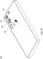
- Fig. 21 is a schematic view of one side of an electronic device 400 according to the 12th embodiment of the present disclosure.
- the electronic device 400 is a smartphone, which include imaging apparatuses 410, 420, 430, 440, 450, 460, 470, 480, 490 and a flash module 401,
- each of the imaging apparatuses 410, 420 can be ultra-wide angle imaging apparatus
- each of the imaging apparatuses 430, 440 can be wide angle imaging apparatus
- each of the imaging apparatuses 450, 460 can be telephoto imaging apparatus
- each of the imaging apparatuses 470, 480 can be telephoto imaging apparatus (which can include light path folding element)
- the imaging apparatus 490 can be TOF module , or can be adaptively adjusted according to the type of the imaging apparatuses, which will not be limited to the arrangement.
Landscapes
- Physics & Mathematics (AREA)
- General Physics & Mathematics (AREA)
- Optics & Photonics (AREA)
- Lenses (AREA)
Claims (10)
- Ensemble système d'imagerie optique comprenant un total de sept lentilles (L1, E2, E3, E4, E5, E6, E7), les sept lentilles (E1, E2, E3, E4, E5, E6, E7) étant, dans l'ordre allant d'un côté objet à un côté image le long d'un trajet optique :une première lentille (E1), une deuxième lentille (E2), une troisième lentille (E3), une quatrième lentille (E4), une cinquième lentille (E5), une sixième lentille (E6) et une septième lentille (E7) ; chacune des sept lentilles (E1, E2, E3, E4, E5, E6, E7) ayant une surface côté objet tournée vers le côté objet et une surface côté image tournée vers le côté image ;la première lentille (E1) ayant un pouvoir de réfraction positif, la surface côté objet de la première lentille (E1) étant convexe dans une région paraxiale de celle-ci, la surface côté image de la première lentille (E1) étant concave dans une région paraxiale de celle-ci ;la deuxième lentille (E2) ayant un pouvoir de réfraction négatif ;la surface côté objet de la troisième lentille (E3) étant convexe dans une région paraxiale de celle-ci ;la cinquième lentille (E5) ayant un pouvoir de réfraction positif ;la sixième lentille (E6) ayant un pouvoir de réfraction négatif ; etla septième lentille (E7) ayant un pouvoir de réfraction négatif ;étant entendu que la surface côté objet et/ou la surface côté image d'au moins une lentille parmi les première (E1) à septième (E7) lentilles comprennent au moins un point d'inflexion (IP) ;étant entendu que le nombre d'Abbe de la quatrième lentille (E4) est V4, le nombre d'Abbe de la cinquième lentille (E5) est V5, le nombre d'Abbe de la sixième lentille (E6) est V6 ; l'épaisseur centrale de la première lentille (E1) est CT1, l'épaisseur centrale de la deuxième lentille (E2) est CT2, l'épaisseur centrale de la troisième lentille (E3) est CT3, l'épaisseur centrale de la quatrième lentille (E4) est CT4, l'épaisseur centrale de la cinquième lentille (E5) est CT5, l'épaisseur centrale de la sixième lentille (E6) est CT6 ; la distance axiale entre la sixième lentille (E6) et la septième lentille (E7) est T67, le nombre f de l'ensemble système d'imagerie optique est Fno, la moitié du champ de vision maximal de l'ensemble système d'imagerie optique est HFOV, la longueur focale de l'ensemble système d'imagerie optique est f, la longueur focale de la troisième lentille (E3) est f3, la longueur focale de la quatrième lentille (E4) est f4, la longueur focale de la septième lentille (E7) est f7 ; le rayon de courbure de la surface côté objet de la septième lentille (E7) est R13, le rayon de courbure de la surface côté image de la septième lentille (E7) est R14, et les conditions suivantes sont satisfaites :


 35,0 degrés < HFOV < 50,0 degrés ;
et
- Ensemble système d'imagerie optique selon la revendication 1, dans lequel les conditions suivantes sont satisfaites :


- Ensemble système d'imagerie optique selon l'une quelconque des revendications 1 et 2, dans lequel la distance axiale entre la surface côté objet de la première lentille (E1) et une surface d'image (IMG) est TL, la distance focale de l'ensemble système d'imagerie optique est f, la distance focale de la cinquième lentille (E5) est f5, et les conditions suivantes sont satisfaites :


- Ensemble système d'imagerie optique selon l'une quelconque des revendications 1 à 3, dans lequel la condition suivante est satisfaite :

- Ensemble système d'imagerie optique selon l'une quelconque des revendications 1 à 4, dans lequel la longueur focale de la premier lentille (E1) est f1, la longueur focale de la sixième lentille (E6) est f6, et la condition suivante est satisfaite :

- Ensemble système d'imagerie optique selon l'une quelconque des revendications 1 à 5, dans lequel la surface côté image de la deuxième lentille (E2) est concave dans une région paraxiale de celle-ci ; la surface côté objet de la cinquième lentille (E5) est concave dans une région paraxiale de celle-ci ; la surface côté image de la cinquième lentille (E5) est convexe dans une région paraxiale de celle-ci.
- Ensemble système d'imagerie optique selon l'une quelconque des revendications 1 à 6, dans lequel la surface côté objet de la sixième lentille (E6) est convexe dans une région paraxiale de celle-ci ; la distance entre au moins un point critique (CP) de la surface côté objet de la sixième lentille (E6) et un axe optique est Yc61, la distance maximale entre une région optique efficace de la surface côté objet de la sixième lentille (E6) et l'axe optique est Y61, et la condition suivante est satisfaite :

- Ensemble système d'imagerie optique selon l'une quelconque des revendications 1 à 7, dans lequel la surface côté objet et/ou la surface côté image de chaque lentille parmi au moins deux lentilles parmi les première (E1) à septième (E7) lentilles comprennent au moins un point d'inflexion (IP) ; la distance maximale entre une région optique efficace de la surface côté objet de la premier lentille (E1) et un axe optique est Y11, la distance maximale entre une région optique efficace de la surface côté image de la septième lentille (E7) et l'axe optique est Y72, et la condition suivante est satisfaite :

- Dispositif d'imagerie (100), comprenant :l'ensemble système d'imagerie optique selon l'une quelconque des revendications 1 à 8, etun capteur d'image (IS) disposé sur la surface d'image (IMG) de l'ensemble système d'imagerie optique.
- Appareil électronique (200), comprenant :
le dispositif d'imagerie (100) selon la revendication 9.
Applications Claiming Priority (1)
| Application Number | Priority Date | Filing Date | Title |
|---|---|---|---|
| TW110133479A TWI800919B (zh) | 2021-09-08 | 2021-09-08 | 光學成像系統組、取像裝置及電子裝置 |
Publications (2)
| Publication Number | Publication Date |
|---|---|
| EP4148478A1 EP4148478A1 (fr) | 2023-03-15 |
| EP4148478B1 true EP4148478B1 (fr) | 2025-07-02 |
Family
ID=81984822
Family Applications (1)
| Application Number | Title | Priority Date | Filing Date |
|---|---|---|---|
| EP22177853.3A Active EP4148478B1 (fr) | 2021-09-08 | 2022-06-08 | Ensemble système d'imagerie optique, appareil d'imagerie et dispositif électronique |
Country Status (4)
| Country | Link |
|---|---|
| US (1) | US12265205B2 (fr) |
| EP (1) | EP4148478B1 (fr) |
| CN (1) | CN115774321B (fr) |
| TW (1) | TWI800919B (fr) |
Families Citing this family (6)
| Publication number | Priority date | Publication date | Assignee | Title |
|---|---|---|---|---|
| US11564002B2 (en) | 2013-03-15 | 2023-01-24 | Sling TV L.L.C. | Automated replacement of video program content |
| CN112578537B (zh) * | 2020-12-29 | 2025-07-18 | 浙江舜宇光学有限公司 | 光学成像系统 |
| KR102842066B1 (ko) * | 2022-09-14 | 2025-08-04 | 삼성전기주식회사 | 촬상 광학계 |
| CN120917359A (zh) * | 2023-04-05 | 2025-11-07 | 三星电子株式会社 | 镜头组件和包括镜头组件的电子装置 |
| US12566320B2 (en) | 2023-06-13 | 2026-03-03 | Bae Systems Information And Electronic Systems Integration Inc. | Panoramic MWIR lens for cooled detectors |
| CN118011599A (zh) | 2024-03-26 | 2024-05-10 | 辰瑞光学(常州)股份有限公司 | 摄像光学镜头 |
Family Cites Families (35)
| Publication number | Priority date | Publication date | Assignee | Title |
|---|---|---|---|---|
| US10018805B2 (en) * | 2013-10-14 | 2018-07-10 | Samsung Electro-Mechanics Co., Ltd. | Lens module |
| TWI534467B (zh) * | 2015-02-17 | 2016-05-21 | 大立光電股份有限公司 | 攝影系統、取像裝置及電子裝置 |
| CN110119021A (zh) | 2016-12-30 | 2019-08-13 | 玉晶光电(厦门)有限公司 | 光学镜片组 |
| TWI614517B (zh) * | 2017-01-04 | 2018-02-11 | 大立光電股份有限公司 | 影像擷取系統、取像裝置及電子裝置 |
| TWI645228B (zh) | 2017-06-03 | 2018-12-21 | 大立光電股份有限公司 | 影像擷取系統鏡頭組、取像裝置及電子裝置 |
| TWI631382B (zh) * | 2017-07-19 | 2018-08-01 | 大立光電股份有限公司 | 攝像系統透鏡組、取像裝置及電子裝置 |
| WO2019037466A1 (fr) * | 2017-08-23 | 2019-02-28 | 浙江舜宇光学有限公司 | Lentille d'appareil photo |
| TWI636295B (zh) * | 2017-11-23 | 2018-09-21 | 大立光電股份有限公司 | 光學取像鏡頭、取像裝置及電子裝置 |
| US10310233B1 (en) * | 2017-12-18 | 2019-06-04 | AAC Technologies Pte. Ltd. | Camera optical lens |
| TWI655474B (zh) | 2017-12-22 | 2019-04-01 | 大立光電股份有限公司 | 取像用光學鏡頭、取像裝置及電子裝置 |
| CN108121054B (zh) | 2017-12-29 | 2020-01-10 | 玉晶光电(厦门)有限公司 | 光学成像镜头 |
| CN109683294B (zh) * | 2018-12-28 | 2021-10-01 | 诚瑞光学(苏州)有限公司 | 摄像光学镜头 |
| CN109828354B (zh) * | 2018-12-31 | 2021-05-04 | 瑞声光学解决方案私人有限公司 | 摄像光学镜头 |
| CN115755345B (zh) * | 2019-01-21 | 2025-05-13 | 大立光电股份有限公司 | 摄像光学透镜组 |
| CN109613684B (zh) * | 2019-02-18 | 2024-06-21 | 浙江舜宇光学有限公司 | 光学成像镜头 |
| US11644642B2 (en) | 2019-02-21 | 2023-05-09 | Samsung Electro-Mechanics Co., Ltd. | Optical imaging system |
| CN110346896B (zh) | 2019-03-30 | 2022-05-13 | 惠州市星聚宇光学有限公司 | 摄像光学透镜组 |
| TWI683126B (zh) * | 2019-04-02 | 2020-01-21 | 大陸商信泰光學(深圳)有限公司 | 成像鏡頭(三十五) |
| CN110673307B (zh) | 2019-10-15 | 2022-05-24 | 玉晶光电(厦门)有限公司 | 光学成像镜头 |
| CN110673309B (zh) | 2019-11-14 | 2022-01-11 | 玉晶光电(厦门)有限公司 | 光学成像镜头 |
| CN113126248B (zh) | 2019-12-31 | 2022-08-26 | 华为技术有限公司 | 光学系统、取像装置及终端设备 |
| CN111538142B (zh) | 2020-07-13 | 2020-10-20 | 瑞声通讯科技(常州)有限公司 | 摄像光学镜头 |
| CN116348798A (zh) | 2020-11-18 | 2023-06-27 | 华为技术有限公司 | 包括内部调光装置的成像镜头 |
| JP7621098B2 (ja) | 2020-11-24 | 2025-01-24 | 東京晨美光学電子株式会社 | 撮像レンズ |
| CN112748524A (zh) | 2020-12-29 | 2021-05-04 | 常州市瑞泰光电有限公司 | 摄像光学镜头 |
| CN112748535A (zh) * | 2020-12-29 | 2021-05-04 | 常州市瑞泰光电有限公司 | 摄像光学镜头 |
| CN112748533A (zh) | 2020-12-29 | 2021-05-04 | 常州市瑞泰光电有限公司 | 摄像光学镜头 |
| CN114690371A (zh) | 2020-12-30 | 2022-07-01 | 华为技术有限公司 | 光学成像系统、摄像模组和终端 |
| CN112904541B (zh) | 2021-02-23 | 2025-05-09 | 江西欧菲光学有限公司 | 光学系统、摄像模组及电子设备 |
| WO2022178657A1 (fr) | 2021-02-23 | 2022-09-01 | 欧菲光集团股份有限公司 | Système optique, module de caméra et dispositif électronique |
| CN113267877B (zh) | 2021-04-14 | 2022-08-19 | 浙江舜宇光学有限公司 | 成像系统 |
| CN214845995U (zh) | 2021-04-14 | 2021-11-23 | 浙江舜宇光学有限公司 | 光学系统 |
| CN113281878B (zh) | 2021-04-28 | 2023-09-05 | 江西晶超光学有限公司 | 光学系统、摄像模组和电子设备 |
| CN113281877B (zh) | 2021-04-28 | 2022-06-24 | 江西晶超光学有限公司 | 光学系统、摄像模组和电子设备 |
| KR102842066B1 (ko) * | 2022-09-14 | 2025-08-04 | 삼성전기주식회사 | 촬상 광학계 |
-
2021
- 2021-09-08 TW TW110133479A patent/TWI800919B/zh active
- 2021-11-12 CN CN202111340743.XA patent/CN115774321B/zh active Active
-
2022
- 2022-04-12 US US17/718,445 patent/US12265205B2/en active Active
- 2022-06-08 EP EP22177853.3A patent/EP4148478B1/fr active Active
Also Published As
| Publication number | Publication date |
|---|---|
| CN115774321A (zh) | 2023-03-10 |
| TW202311796A (zh) | 2023-03-16 |
| US20230070553A1 (en) | 2023-03-09 |
| EP4148478A1 (fr) | 2023-03-15 |
| CN115774321B (zh) | 2026-04-24 |
| TWI800919B (zh) | 2023-05-01 |
| US12265205B2 (en) | 2025-04-01 |
Similar Documents
| Publication | Publication Date | Title |
|---|---|---|
| US12216255B2 (en) | Photographing optical lens assembly including eight lenses of +−+−−++−, +−++−++−, ++++−++− or +−+−+−+−refractive powers, imaging apparatus and electronic device | |
| US11982875B2 (en) | Image capturing lens assembly, imaging apparatus and electronic device | |
| US11789236B2 (en) | Photographing optical lens assembly, imaging apparatus and electronic device | |
| US11249282B2 (en) | Photographing optical lens assembly, imaging apparatus and electronic device | |
| EP4148478B1 (fr) | Ensemble système d'imagerie optique, appareil d'imagerie et dispositif électronique | |
| EP4105701B1 (fr) | Ensemble lentille de capture d'imagerie optique, unité de capture d'images et dispositif électronique | |
| US20230121630A1 (en) | Imaging system lens assembly, imaging apparatus and electronic device | |
| US12044829B2 (en) | Image capturing lens assembly, imaging apparatus and electronic device | |
| US11899172B2 (en) | Imaging optical lens assembly including five lenses +−++−, −++−, −−++−, +−+++, +++−+, +−+−+, +−+−−, or −++−+ of refractive powers, imaging apparatus and electronic device | |
| EP4001985A2 (fr) | Système de lentille d'imagerie optique, unité de capture d'image et dispositif électronique | |
| US12117596B2 (en) | Image lens assembly, imaging apparatus and electronic device | |
| US11487089B2 (en) | Image capturing optical lens assembly including five lenses of +−++− or +−−+− refractive powers, imaging apparatus and electronic device | |
| US20250004250A1 (en) | Image capturing system lens assembly, imaging apparatus and electronic device | |
| US11966031B2 (en) | Image lens assembly, zoom imaging apparatus and electronic device | |
| EP4224234B1 (fr) | Ensemble lentille de système optique d'imagerie, appareil d'imagerie et dispositif électronique | |
| EP4177656B1 (fr) | Assemblage de lentilles pour un système de capture d'images, appareil d'imagerie et dispositif électronique | |
| EP4071534B1 (fr) | Ensemble lentille d'imagerie optique, unité de capture d'image et dispositif électronique | |
| US20240264410A1 (en) | Photographing system lens assembly, imaging apparatus and electronic device | |
| EP4293407B1 (fr) | Ensemble lentille de système d'imagerie, appareil d'imagerie et dispositif électronique | |
| US12000991B2 (en) | Optical image capturing lens assembly, imaging apparatus and electronic device | |
| EP4296743B1 (fr) | Ensemble lentille d'imagerie, unité de capture d'images et dispositif électronique | |
| EP4191314B1 (fr) | Système d'imagerie optique, unité de capture d'image et dispositif électronique | |
| US20260072251A1 (en) | Imaging optical lens system, imaging apparatus and electronic device |
Legal Events
| Date | Code | Title | Description |
|---|---|---|---|
| PUAI | Public reference made under article 153(3) epc to a published international application that has entered the european phase |
Free format text: ORIGINAL CODE: 0009012 |
|
| STAA | Information on the status of an ep patent application or granted ep patent |
Free format text: STATUS: REQUEST FOR EXAMINATION WAS MADE |
|
| 17P | Request for examination filed |
Effective date: 20220608 |
|
| AK | Designated contracting states |
Kind code of ref document: A1 Designated state(s): AL AT BE BG CH CY CZ DE DK EE ES FI FR GB GR HR HU IE IS IT LI LT LU LV MC MK MT NL NO PL PT RO RS SE SI SK SM TR |
|
| GRAP | Despatch of communication of intention to grant a patent |
Free format text: ORIGINAL CODE: EPIDOSNIGR1 |
|
| STAA | Information on the status of an ep patent application or granted ep patent |
Free format text: STATUS: GRANT OF PATENT IS INTENDED |
|
| INTG | Intention to grant announced |
Effective date: 20250203 |
|
| GRAS | Grant fee paid |
Free format text: ORIGINAL CODE: EPIDOSNIGR3 |
|
| GRAA | (expected) grant |
Free format text: ORIGINAL CODE: 0009210 |
|
| STAA | Information on the status of an ep patent application or granted ep patent |
Free format text: STATUS: THE PATENT HAS BEEN GRANTED |
|
| P01 | Opt-out of the competence of the unified patent court (upc) registered |
Free format text: CASE NUMBER: APP_21752/2025 Effective date: 20250507 |
|
| AK | Designated contracting states |
Kind code of ref document: B1 Designated state(s): AL AT BE BG CH CY CZ DE DK EE ES FI FR GB GR HR HU IE IS IT LI LT LU LV MC MK MT NL NO PL PT RO RS SE SI SK SM TR |
|
| REG | Reference to a national code |
Ref country code: GB Ref legal event code: FG4D |
|
| REG | Reference to a national code |
Ref country code: CH Ref legal event code: EP |
|
| REG | Reference to a national code |
Ref country code: DE Ref legal event code: R096 Ref document number: 602022016729 Country of ref document: DE |
|
| REG | Reference to a national code |
Ref country code: IE Ref legal event code: FG4D |
|
| REG | Reference to a national code |
Ref country code: NL Ref legal event code: FP |
|
| PG25 | Lapsed in a contracting state [announced via postgrant information from national office to epo] |
Ref country code: PT Free format text: LAPSE BECAUSE OF FAILURE TO SUBMIT A TRANSLATION OF THE DESCRIPTION OR TO PAY THE FEE WITHIN THE PRESCRIBED TIME-LIMIT Effective date: 20251103 |
|
| REG | Reference to a national code |
Ref country code: AT Ref legal event code: MK05 Ref document number: 1809872 Country of ref document: AT Kind code of ref document: T Effective date: 20250702 |
|
| PG25 | Lapsed in a contracting state [announced via postgrant information from national office to epo] |
Ref country code: IS Free format text: LAPSE BECAUSE OF FAILURE TO SUBMIT A TRANSLATION OF THE DESCRIPTION OR TO PAY THE FEE WITHIN THE PRESCRIBED TIME-LIMIT Effective date: 20251102 |
|
| PG25 | Lapsed in a contracting state [announced via postgrant information from national office to epo] |
Ref country code: NO Free format text: LAPSE BECAUSE OF FAILURE TO SUBMIT A TRANSLATION OF THE DESCRIPTION OR TO PAY THE FEE WITHIN THE PRESCRIBED TIME-LIMIT Effective date: 20251002 |
|
| REG | Reference to a national code |
Ref country code: LT Ref legal event code: MG9D |
|
| PG25 | Lapsed in a contracting state [announced via postgrant information from national office to epo] |
Ref country code: AT Free format text: LAPSE BECAUSE OF FAILURE TO SUBMIT A TRANSLATION OF THE DESCRIPTION OR TO PAY THE FEE WITHIN THE PRESCRIBED TIME-LIMIT Effective date: 20250702 |
|
| PG25 | Lapsed in a contracting state [announced via postgrant information from national office to epo] |
Ref country code: FI Free format text: LAPSE BECAUSE OF FAILURE TO SUBMIT A TRANSLATION OF THE DESCRIPTION OR TO PAY THE FEE WITHIN THE PRESCRIBED TIME-LIMIT Effective date: 20250702 |
|
| PG25 | Lapsed in a contracting state [announced via postgrant information from national office to epo] |
Ref country code: HR Free format text: LAPSE BECAUSE OF FAILURE TO SUBMIT A TRANSLATION OF THE DESCRIPTION OR TO PAY THE FEE WITHIN THE PRESCRIBED TIME-LIMIT Effective date: 20250702 |
|
| PG25 | Lapsed in a contracting state [announced via postgrant information from national office to epo] |
Ref country code: GR Free format text: LAPSE BECAUSE OF FAILURE TO SUBMIT A TRANSLATION OF THE DESCRIPTION OR TO PAY THE FEE WITHIN THE PRESCRIBED TIME-LIMIT Effective date: 20251003 |
|
| PG25 | Lapsed in a contracting state [announced via postgrant information from national office to epo] |
Ref country code: CZ Free format text: LAPSE BECAUSE OF FAILURE TO SUBMIT A TRANSLATION OF THE DESCRIPTION OR TO PAY THE FEE WITHIN THE PRESCRIBED TIME-LIMIT Effective date: 20250702 Ref country code: SE Free format text: LAPSE BECAUSE OF FAILURE TO SUBMIT A TRANSLATION OF THE DESCRIPTION OR TO PAY THE FEE WITHIN THE PRESCRIBED TIME-LIMIT Effective date: 20250702 |
|
| PG25 | Lapsed in a contracting state [announced via postgrant information from national office to epo] |
Ref country code: LV Free format text: LAPSE BECAUSE OF FAILURE TO SUBMIT A TRANSLATION OF THE DESCRIPTION OR TO PAY THE FEE WITHIN THE PRESCRIBED TIME-LIMIT Effective date: 20250702 |
|
| PG25 | Lapsed in a contracting state [announced via postgrant information from national office to epo] |
Ref country code: PL Free format text: LAPSE BECAUSE OF FAILURE TO SUBMIT A TRANSLATION OF THE DESCRIPTION OR TO PAY THE FEE WITHIN THE PRESCRIBED TIME-LIMIT Effective date: 20250702 Ref country code: BG Free format text: LAPSE BECAUSE OF FAILURE TO SUBMIT A TRANSLATION OF THE DESCRIPTION OR TO PAY THE FEE WITHIN THE PRESCRIBED TIME-LIMIT Effective date: 20250702 |
|
| PG25 | Lapsed in a contracting state [announced via postgrant information from national office to epo] |
Ref country code: RS Free format text: LAPSE BECAUSE OF FAILURE TO SUBMIT A TRANSLATION OF THE DESCRIPTION OR TO PAY THE FEE WITHIN THE PRESCRIBED TIME-LIMIT Effective date: 20251002 |
|
| PG25 | Lapsed in a contracting state [announced via postgrant information from national office to epo] |
Ref country code: ES Free format text: LAPSE BECAUSE OF FAILURE TO SUBMIT A TRANSLATION OF THE DESCRIPTION OR TO PAY THE FEE WITHIN THE PRESCRIBED TIME-LIMIT Effective date: 20250702 |
|
| PG25 | Lapsed in a contracting state [announced via postgrant information from national office to epo] |
Ref country code: SM Free format text: LAPSE BECAUSE OF FAILURE TO SUBMIT A TRANSLATION OF THE DESCRIPTION OR TO PAY THE FEE WITHIN THE PRESCRIBED TIME-LIMIT Effective date: 20250702 |
|
| PG25 | Lapsed in a contracting state [announced via postgrant information from national office to epo] |
Ref country code: DK Free format text: LAPSE BECAUSE OF FAILURE TO SUBMIT A TRANSLATION OF THE DESCRIPTION OR TO PAY THE FEE WITHIN THE PRESCRIBED TIME-LIMIT Effective date: 20250702 |
|
| PG25 | Lapsed in a contracting state [announced via postgrant information from national office to epo] |
Ref country code: IT Free format text: LAPSE BECAUSE OF FAILURE TO SUBMIT A TRANSLATION OF THE DESCRIPTION OR TO PAY THE FEE WITHIN THE PRESCRIBED TIME-LIMIT Effective date: 20250702 |
|
| PG25 | Lapsed in a contracting state [announced via postgrant information from national office to epo] |
Ref country code: SK Free format text: LAPSE BECAUSE OF FAILURE TO SUBMIT A TRANSLATION OF THE DESCRIPTION OR TO PAY THE FEE WITHIN THE PRESCRIBED TIME-LIMIT Effective date: 20250702 Ref country code: EE Free format text: LAPSE BECAUSE OF FAILURE TO SUBMIT A TRANSLATION OF THE DESCRIPTION OR TO PAY THE FEE WITHIN THE PRESCRIBED TIME-LIMIT Effective date: 20250702 |