EP4148720B1 - Panneau d'affichage et appareil d'affichage - Google Patents
Panneau d'affichage et appareil d'affichage Download PDFInfo
- Publication number
- EP4148720B1 EP4148720B1 EP21733700.5A EP21733700A EP4148720B1 EP 4148720 B1 EP4148720 B1 EP 4148720B1 EP 21733700 A EP21733700 A EP 21733700A EP 4148720 B1 EP4148720 B1 EP 4148720B1
- Authority
- EP
- European Patent Office
- Prior art keywords
- transistor
- base substrate
- light emitting
- orthographic projection
- emitting control
- Prior art date
- Legal status (The legal status is an assumption and is not a legal conclusion. Google has not performed a legal analysis and makes no representation as to the accuracy of the status listed.)
- Active
Links
Images







Classifications
-
- G—PHYSICS
- G09—EDUCATION; CRYPTOGRAPHY; DISPLAY; ADVERTISING; SEALS
- G09G—ARRANGEMENTS OR CIRCUITS FOR CONTROL OF INDICATING DEVICES USING STATIC MEANS TO PRESENT VARIABLE INFORMATION
- G09G3/00—Control arrangements or circuits, of interest only in connection with visual indicators other than cathode-ray tubes
- G09G3/20—Control arrangements or circuits, of interest only in connection with visual indicators other than cathode-ray tubes for presentation of an assembly of a number of characters, e.g. a page, by composing the assembly by combination of individual elements arranged in a matrix no fixed position being assigned to or needed to be assigned to the individual characters or partial characters
- G09G3/22—Control arrangements or circuits, of interest only in connection with visual indicators other than cathode-ray tubes for presentation of an assembly of a number of characters, e.g. a page, by composing the assembly by combination of individual elements arranged in a matrix no fixed position being assigned to or needed to be assigned to the individual characters or partial characters using controlled light sources
- G09G3/30—Control arrangements or circuits, of interest only in connection with visual indicators other than cathode-ray tubes for presentation of an assembly of a number of characters, e.g. a page, by composing the assembly by combination of individual elements arranged in a matrix no fixed position being assigned to or needed to be assigned to the individual characters or partial characters using controlled light sources using electroluminescent panels
- G09G3/32—Control arrangements or circuits, of interest only in connection with visual indicators other than cathode-ray tubes for presentation of an assembly of a number of characters, e.g. a page, by composing the assembly by combination of individual elements arranged in a matrix no fixed position being assigned to or needed to be assigned to the individual characters or partial characters using controlled light sources using electroluminescent panels semiconductive, e.g. using light-emitting diodes [LED]
- G09G3/3208—Control arrangements or circuits, of interest only in connection with visual indicators other than cathode-ray tubes for presentation of an assembly of a number of characters, e.g. a page, by composing the assembly by combination of individual elements arranged in a matrix no fixed position being assigned to or needed to be assigned to the individual characters or partial characters using controlled light sources using electroluminescent panels semiconductive, e.g. using light-emitting diodes [LED] organic, e.g. using organic light-emitting diodes [OLED]
- G09G3/3225—Control arrangements or circuits, of interest only in connection with visual indicators other than cathode-ray tubes for presentation of an assembly of a number of characters, e.g. a page, by composing the assembly by combination of individual elements arranged in a matrix no fixed position being assigned to or needed to be assigned to the individual characters or partial characters using controlled light sources using electroluminescent panels semiconductive, e.g. using light-emitting diodes [LED] organic, e.g. using organic light-emitting diodes [OLED] using an active matrix
- G09G3/3233—Control arrangements or circuits, of interest only in connection with visual indicators other than cathode-ray tubes for presentation of an assembly of a number of characters, e.g. a page, by composing the assembly by combination of individual elements arranged in a matrix no fixed position being assigned to or needed to be assigned to the individual characters or partial characters using controlled light sources using electroluminescent panels semiconductive, e.g. using light-emitting diodes [LED] organic, e.g. using organic light-emitting diodes [OLED] using an active matrix with pixel circuitry controlling the current through the light-emitting element
-
- H—ELECTRICITY
- H10—SEMICONDUCTOR DEVICES; ELECTRIC SOLID-STATE DEVICES NOT OTHERWISE PROVIDED FOR
- H10K—ORGANIC ELECTRIC SOLID-STATE DEVICES
- H10K59/00—Integrated devices, or assemblies of multiple devices, comprising at least one organic light-emitting element covered by group H10K50/00
- H10K59/10—OLED displays
- H10K59/12—Active-matrix OLED [AMOLED] displays
- H10K59/131—Interconnections, e.g. wiring lines or terminals
-
- G—PHYSICS
- G09—EDUCATION; CRYPTOGRAPHY; DISPLAY; ADVERTISING; SEALS
- G09G—ARRANGEMENTS OR CIRCUITS FOR CONTROL OF INDICATING DEVICES USING STATIC MEANS TO PRESENT VARIABLE INFORMATION
- G09G3/00—Control arrangements or circuits, of interest only in connection with visual indicators other than cathode-ray tubes
- G09G3/20—Control arrangements or circuits, of interest only in connection with visual indicators other than cathode-ray tubes for presentation of an assembly of a number of characters, e.g. a page, by composing the assembly by combination of individual elements arranged in a matrix no fixed position being assigned to or needed to be assigned to the individual characters or partial characters
- G09G3/22—Control arrangements or circuits, of interest only in connection with visual indicators other than cathode-ray tubes for presentation of an assembly of a number of characters, e.g. a page, by composing the assembly by combination of individual elements arranged in a matrix no fixed position being assigned to or needed to be assigned to the individual characters or partial characters using controlled light sources
- G09G3/30—Control arrangements or circuits, of interest only in connection with visual indicators other than cathode-ray tubes for presentation of an assembly of a number of characters, e.g. a page, by composing the assembly by combination of individual elements arranged in a matrix no fixed position being assigned to or needed to be assigned to the individual characters or partial characters using controlled light sources using electroluminescent panels
- G09G3/32—Control arrangements or circuits, of interest only in connection with visual indicators other than cathode-ray tubes for presentation of an assembly of a number of characters, e.g. a page, by composing the assembly by combination of individual elements arranged in a matrix no fixed position being assigned to or needed to be assigned to the individual characters or partial characters using controlled light sources using electroluminescent panels semiconductive, e.g. using light-emitting diodes [LED]
- G09G3/3208—Control arrangements or circuits, of interest only in connection with visual indicators other than cathode-ray tubes for presentation of an assembly of a number of characters, e.g. a page, by composing the assembly by combination of individual elements arranged in a matrix no fixed position being assigned to or needed to be assigned to the individual characters or partial characters using controlled light sources using electroluminescent panels semiconductive, e.g. using light-emitting diodes [LED] organic, e.g. using organic light-emitting diodes [OLED]
- G09G3/3225—Control arrangements or circuits, of interest only in connection with visual indicators other than cathode-ray tubes for presentation of an assembly of a number of characters, e.g. a page, by composing the assembly by combination of individual elements arranged in a matrix no fixed position being assigned to or needed to be assigned to the individual characters or partial characters using controlled light sources using electroluminescent panels semiconductive, e.g. using light-emitting diodes [LED] organic, e.g. using organic light-emitting diodes [OLED] using an active matrix
-
- G—PHYSICS
- G09—EDUCATION; CRYPTOGRAPHY; DISPLAY; ADVERTISING; SEALS
- G09G—ARRANGEMENTS OR CIRCUITS FOR CONTROL OF INDICATING DEVICES USING STATIC MEANS TO PRESENT VARIABLE INFORMATION
- G09G3/00—Control arrangements or circuits, of interest only in connection with visual indicators other than cathode-ray tubes
- G09G3/20—Control arrangements or circuits, of interest only in connection with visual indicators other than cathode-ray tubes for presentation of an assembly of a number of characters, e.g. a page, by composing the assembly by combination of individual elements arranged in a matrix no fixed position being assigned to or needed to be assigned to the individual characters or partial characters
- G09G3/22—Control arrangements or circuits, of interest only in connection with visual indicators other than cathode-ray tubes for presentation of an assembly of a number of characters, e.g. a page, by composing the assembly by combination of individual elements arranged in a matrix no fixed position being assigned to or needed to be assigned to the individual characters or partial characters using controlled light sources
- G09G3/30—Control arrangements or circuits, of interest only in connection with visual indicators other than cathode-ray tubes for presentation of an assembly of a number of characters, e.g. a page, by composing the assembly by combination of individual elements arranged in a matrix no fixed position being assigned to or needed to be assigned to the individual characters or partial characters using controlled light sources using electroluminescent panels
- G09G3/32—Control arrangements or circuits, of interest only in connection with visual indicators other than cathode-ray tubes for presentation of an assembly of a number of characters, e.g. a page, by composing the assembly by combination of individual elements arranged in a matrix no fixed position being assigned to or needed to be assigned to the individual characters or partial characters using controlled light sources using electroluminescent panels semiconductive, e.g. using light-emitting diodes [LED]
- G09G3/3208—Control arrangements or circuits, of interest only in connection with visual indicators other than cathode-ray tubes for presentation of an assembly of a number of characters, e.g. a page, by composing the assembly by combination of individual elements arranged in a matrix no fixed position being assigned to or needed to be assigned to the individual characters or partial characters using controlled light sources using electroluminescent panels semiconductive, e.g. using light-emitting diodes [LED] organic, e.g. using organic light-emitting diodes [OLED]
- G09G3/3225—Control arrangements or circuits, of interest only in connection with visual indicators other than cathode-ray tubes for presentation of an assembly of a number of characters, e.g. a page, by composing the assembly by combination of individual elements arranged in a matrix no fixed position being assigned to or needed to be assigned to the individual characters or partial characters using controlled light sources using electroluminescent panels semiconductive, e.g. using light-emitting diodes [LED] organic, e.g. using organic light-emitting diodes [OLED] using an active matrix
- G09G3/3258—Control arrangements or circuits, of interest only in connection with visual indicators other than cathode-ray tubes for presentation of an assembly of a number of characters, e.g. a page, by composing the assembly by combination of individual elements arranged in a matrix no fixed position being assigned to or needed to be assigned to the individual characters or partial characters using controlled light sources using electroluminescent panels semiconductive, e.g. using light-emitting diodes [LED] organic, e.g. using organic light-emitting diodes [OLED] using an active matrix with pixel circuitry controlling the voltage across the light-emitting element
-
- H—ELECTRICITY
- H10—SEMICONDUCTOR DEVICES; ELECTRIC SOLID-STATE DEVICES NOT OTHERWISE PROVIDED FOR
- H10D—INORGANIC ELECTRIC SEMICONDUCTOR DEVICES
- H10D86/00—Integrated devices formed in or on insulating or conducting substrates, e.g. formed in silicon-on-insulator [SOI] substrates or on stainless steel or glass substrates
-
- H—ELECTRICITY
- H10—SEMICONDUCTOR DEVICES; ELECTRIC SOLID-STATE DEVICES NOT OTHERWISE PROVIDED FOR
- H10D—INORGANIC ELECTRIC SEMICONDUCTOR DEVICES
- H10D86/00—Integrated devices formed in or on insulating or conducting substrates, e.g. formed in silicon-on-insulator [SOI] substrates or on stainless steel or glass substrates
- H10D86/40—Integrated devices formed in or on insulating or conducting substrates, e.g. formed in silicon-on-insulator [SOI] substrates or on stainless steel or glass substrates characterised by multiple TFTs
- H10D86/421—Integrated devices formed in or on insulating or conducting substrates, e.g. formed in silicon-on-insulator [SOI] substrates or on stainless steel or glass substrates characterised by multiple TFTs having a particular composition, shape or crystalline structure of the active layer
-
- H—ELECTRICITY
- H10—SEMICONDUCTOR DEVICES; ELECTRIC SOLID-STATE DEVICES NOT OTHERWISE PROVIDED FOR
- H10D—INORGANIC ELECTRIC SEMICONDUCTOR DEVICES
- H10D86/00—Integrated devices formed in or on insulating or conducting substrates, e.g. formed in silicon-on-insulator [SOI] substrates or on stainless steel or glass substrates
- H10D86/40—Integrated devices formed in or on insulating or conducting substrates, e.g. formed in silicon-on-insulator [SOI] substrates or on stainless steel or glass substrates characterised by multiple TFTs
- H10D86/421—Integrated devices formed in or on insulating or conducting substrates, e.g. formed in silicon-on-insulator [SOI] substrates or on stainless steel or glass substrates characterised by multiple TFTs having a particular composition, shape or crystalline structure of the active layer
- H10D86/423—Integrated devices formed in or on insulating or conducting substrates, e.g. formed in silicon-on-insulator [SOI] substrates or on stainless steel or glass substrates characterised by multiple TFTs having a particular composition, shape or crystalline structure of the active layer comprising semiconductor materials not belonging to the Group IV, e.g. InGaZnO
-
- H—ELECTRICITY
- H10—SEMICONDUCTOR DEVICES; ELECTRIC SOLID-STATE DEVICES NOT OTHERWISE PROVIDED FOR
- H10D—INORGANIC ELECTRIC SEMICONDUCTOR DEVICES
- H10D86/00—Integrated devices formed in or on insulating or conducting substrates, e.g. formed in silicon-on-insulator [SOI] substrates or on stainless steel or glass substrates
- H10D86/40—Integrated devices formed in or on insulating or conducting substrates, e.g. formed in silicon-on-insulator [SOI] substrates or on stainless steel or glass substrates characterised by multiple TFTs
- H10D86/481—Integrated devices formed in or on insulating or conducting substrates, e.g. formed in silicon-on-insulator [SOI] substrates or on stainless steel or glass substrates characterised by multiple TFTs integrated with passive devices, e.g. auxiliary capacitors
-
- H—ELECTRICITY
- H10—SEMICONDUCTOR DEVICES; ELECTRIC SOLID-STATE DEVICES NOT OTHERWISE PROVIDED FOR
- H10D—INORGANIC ELECTRIC SEMICONDUCTOR DEVICES
- H10D86/00—Integrated devices formed in or on insulating or conducting substrates, e.g. formed in silicon-on-insulator [SOI] substrates or on stainless steel or glass substrates
- H10D86/40—Integrated devices formed in or on insulating or conducting substrates, e.g. formed in silicon-on-insulator [SOI] substrates or on stainless steel or glass substrates characterised by multiple TFTs
- H10D86/60—Integrated devices formed in or on insulating or conducting substrates, e.g. formed in silicon-on-insulator [SOI] substrates or on stainless steel or glass substrates characterised by multiple TFTs wherein the TFTs are in active matrices
-
- H—ELECTRICITY
- H10—SEMICONDUCTOR DEVICES; ELECTRIC SOLID-STATE DEVICES NOT OTHERWISE PROVIDED FOR
- H10K—ORGANIC ELECTRIC SOLID-STATE DEVICES
- H10K59/00—Integrated devices, or assemblies of multiple devices, comprising at least one organic light-emitting element covered by group H10K50/00
- H10K59/10—OLED displays
- H10K59/12—Active-matrix OLED [AMOLED] displays
- H10K59/121—Active-matrix OLED [AMOLED] displays characterised by the geometry or disposition of pixel elements
-
- H—ELECTRICITY
- H10—SEMICONDUCTOR DEVICES; ELECTRIC SOLID-STATE DEVICES NOT OTHERWISE PROVIDED FOR
- H10K—ORGANIC ELECTRIC SOLID-STATE DEVICES
- H10K59/00—Integrated devices, or assemblies of multiple devices, comprising at least one organic light-emitting element covered by group H10K50/00
- H10K59/10—OLED displays
- H10K59/12—Active-matrix OLED [AMOLED] displays
- H10K59/121—Active-matrix OLED [AMOLED] displays characterised by the geometry or disposition of pixel elements
- H10K59/1216—Active-matrix OLED [AMOLED] displays characterised by the geometry or disposition of pixel elements the pixel elements being capacitors
-
- G—PHYSICS
- G09—EDUCATION; CRYPTOGRAPHY; DISPLAY; ADVERTISING; SEALS
- G09G—ARRANGEMENTS OR CIRCUITS FOR CONTROL OF INDICATING DEVICES USING STATIC MEANS TO PRESENT VARIABLE INFORMATION
- G09G2300/00—Aspects of the constitution of display devices
- G09G2300/04—Structural and physical details of display devices
- G09G2300/0421—Structural details of the set of electrodes
- G09G2300/0426—Layout of electrodes and connections
-
- G—PHYSICS
- G09—EDUCATION; CRYPTOGRAPHY; DISPLAY; ADVERTISING; SEALS
- G09G—ARRANGEMENTS OR CIRCUITS FOR CONTROL OF INDICATING DEVICES USING STATIC MEANS TO PRESENT VARIABLE INFORMATION
- G09G2300/00—Aspects of the constitution of display devices
- G09G2300/04—Structural and physical details of display devices
- G09G2300/0421—Structural details of the set of electrodes
- G09G2300/043—Compensation electrodes or other additional electrodes in matrix displays related to distortions or compensation signals, e.g. for modifying TFT threshold voltage in column driver
-
- G—PHYSICS
- G09—EDUCATION; CRYPTOGRAPHY; DISPLAY; ADVERTISING; SEALS
- G09G—ARRANGEMENTS OR CIRCUITS FOR CONTROL OF INDICATING DEVICES USING STATIC MEANS TO PRESENT VARIABLE INFORMATION
- G09G2300/00—Aspects of the constitution of display devices
- G09G2300/08—Active matrix structure, i.e. with use of active elements, inclusive of non-linear two terminal elements, in the pixels together with light emitting or modulating elements
- G09G2300/0809—Several active elements per pixel in active matrix panels
- G09G2300/0819—Several active elements per pixel in active matrix panels used for counteracting undesired variations, e.g. feedback or autozeroing
-
- G—PHYSICS
- G09—EDUCATION; CRYPTOGRAPHY; DISPLAY; ADVERTISING; SEALS
- G09G—ARRANGEMENTS OR CIRCUITS FOR CONTROL OF INDICATING DEVICES USING STATIC MEANS TO PRESENT VARIABLE INFORMATION
- G09G2300/00—Aspects of the constitution of display devices
- G09G2300/08—Active matrix structure, i.e. with use of active elements, inclusive of non-linear two terminal elements, in the pixels together with light emitting or modulating elements
- G09G2300/0809—Several active elements per pixel in active matrix panels
- G09G2300/0842—Several active elements per pixel in active matrix panels forming a memory circuit, e.g. a dynamic memory with one capacitor
-
- G—PHYSICS
- G09—EDUCATION; CRYPTOGRAPHY; DISPLAY; ADVERTISING; SEALS
- G09G—ARRANGEMENTS OR CIRCUITS FOR CONTROL OF INDICATING DEVICES USING STATIC MEANS TO PRESENT VARIABLE INFORMATION
- G09G2300/00—Aspects of the constitution of display devices
- G09G2300/08—Active matrix structure, i.e. with use of active elements, inclusive of non-linear two terminal elements, in the pixels together with light emitting or modulating elements
- G09G2300/0876—Supplementary capacities in pixels having special driving circuits and electrodes instead of being connected to common electrode or ground; Use of additional capacitively coupled compensation electrodes
-
- G—PHYSICS
- G09—EDUCATION; CRYPTOGRAPHY; DISPLAY; ADVERTISING; SEALS
- G09G—ARRANGEMENTS OR CIRCUITS FOR CONTROL OF INDICATING DEVICES USING STATIC MEANS TO PRESENT VARIABLE INFORMATION
- G09G2320/00—Control of display operating conditions
- G09G2320/04—Maintaining the quality of display appearance
- G09G2320/043—Preventing or counteracting the effects of ageing
- G09G2320/045—Compensation of drifts in the characteristics of light emitting or modulating elements
Definitions
- This disclosure relates to the technical field of display, in particular to a display panel and a display device.
- An electroluminescent diode such as an OLED (Organic Light Emitting Diode) and a QLED (Quantum Dot Light Emitting Diode) has the advantages of self luminescence and low energy consumption so as to become one of hot spots in the field of application research of electroluminescent display devices at present.
- CN 111128080 A discloses a display panel, as known in the prior art.
- Embodiments of the disclosure provide a display panel, including
- an orthographic projection of the second power line part on the base substrate covers an orthographic projection of the second connection part on the base substrate; the orthographic projection of the second power line part on the base substrate exceeds edges of two sides, in a second direction, of an orthographic projection of the gate electrode of the driving transistor on the base substrate, and exceeds edges of two sides, in the second direction, of an orthographic projection of the storage conducting part on the base substrate.
- the first conducting layer further includes a plurality of third scanning lines spaced from each other, the third scanning lines are extended in a first direction and arranged in the second direction.
- the sub-pixel further includes a data writing transistor a gate electrode of the data writing transistor is electrically connected to the third scanning line.
- An orthographic projection of the third scanning line on the base substrate and the orthographic projection of the second power line part on the base substrate have an overlapping region.
- the second conducting layer further includes a plurality of auxiliary scanning lines spaced from each other.
- an orthographic projection of the auxiliary scanning line on the base substrate and an orthographic projection of the active oxide layer of the oxide transistor on the base substrate has a sixth overlapping region, and the orthographic projection of the second power line part on the base substrate is overlapped with the sixth overlapping region.
- the sub-pixel further includes a first light emitting control transistor and a second light emitting control transistor.
- the silicon semiconductor layer further includes an active silicon layer of the first light emitting control transistor and an active silicon layer of the second light emitting control transistor.
- the first conducting layer further includes a gate electrode of the first light emitting control transistor and a gate electrode of the second light emitting control transistor.
- the first power line part is electrically connected to a first electrode of the first light emitting control transistor
- a second electrode of the first light emitting control transistor is electrically connected to a first electrode of the driving transistor
- a first electrode of the second light emitting control transistor is electrically connected to a second electrode of the driving transistor
- a second electrode of the second light emitting control transistor is electrically connected to a first electrode of a light emitting device.
- the first conducting layer further includes a plurality of light emitting control lines spaced from each other.
- an orthographic projection of the light emitting control line on the base substrate is at a side, facing away from an orthographic projection of the auxiliary scanning line on the base substrate, of the orthographic projection of the gate electrode of the driving transistor on the base substrate.
- the light emitting control line is electrically connected to the gate electrode of the first light emitting control transistor and the gate electrode of the second light emitting control transistor.
- the orthographic projection of the second power line part on the base substrate and the orthographic projection of the light emitting control line on the base substrate have an overlapping region.
- the second connection part includes a first conducting part and a first main part.
- the first conducting part is electrically connected to the first main part; the first conducting part is electrically connected to the active oxide layer of the oxide transistor.
- An orthographic projection of the first main part on the base substrate and the orthographic projection of the gate electrode of the driving transistor on the base substrate have an overlapping region, and the orthographic projection of the first main part on the base substrate is not overlapped with the orthographic projection of the third scanning line on the base substrate.
- a minimum straight-line distance between the orthographic projection of the first main part on the base substrate and an orthographic projection of the first power line part on the base substrate is less than a minimum straight-line distance between the orthographic projection of the first main part on the base substrate and an orthographic projection of the gate electrode of the first light emitting control transistor.
- the third conducting layer further includes a first connection part spaced from the first power line part and the second connection part.
- the first connection part is electrically connected to the active oxide layer of the oxide transistor.
- a distance between the first connection part and the first conducting part is larger than a threshold.
- embodiments of the disclosure further provides another display panel, includes:
- the active oxide layer of the oxide transistor is electrically connected to the gate electrode of the driving transistor through the second connection part; a first electrode of the initialization transistor is electrically connected to the gate electrode of the driving transistor through the first connection part and the second connection part; and the first connection part includes a part with an extension direction substantially parallel to the first direction.
- the first connection part includes a first sub-connection part electrically connected to the active oxide layer of the oxide transistor.
- An extension direction of the first sub-connection part is substantially parallel to the first direction, and intersects with an extension direction of the active oxide layer of the oxide transistor.
- the first connection part further includes a second sub-connection part electrically connected to the first sub-connection part.
- An extension direction of the second sub-connection part is substantially parallel to the extension direction of the active oxide layer of the oxide transistor.
- an orthographic projection of the second connection part on the base substrate is within an orthographic projection of the gate electrode of the driving transistor on the base substrate.
- the sub-pixel further includes an initialization line; the initialization transistor is electrically connected to the initialization line; and an initialization signal is transmitted to gate electrode of the driving transistor at least through the first sub-connection part and the second connection part.
- the second conducting layer further includes storage conducting parts; the third conducting layer further includes first power line parts spaced from each other; and the first power line parts are electrically connected to the storage conducting parts.
- the display panel further includes a fourth conducting layer, at a side, facing away from the base substrate, of the third conducting layer, the fourth conducting layer including a second power line part.
- the first power line part is electrically connected to the second power line part.
- an orthographic projection of the second power line part on the base substrate covers an orthographic projection of the second connection part on the base substrate; the orthographic projection of the second power line part on the base substrate exceeds edges of two sides, in a second direction, of the orthographic projection of the gate electrode of the driving transistor on the base substrate, and exceeds edges of two sides, in the second direction, of an orthographic projection of the storage conducting part on the base substrate.
- the first conducting layer further includes a plurality of third scanning lines spaced from each other, the third scanning lines are extended in a first direction and arranged in the second direction.
- the sub-pixel circuit further includes a data writing transistor, a gate electrode of the data writing transistor is electrically connected to the third scanning line.
- An orthographic projection of the third scanning line on the base substrate and the orthographic projection of the second connection part on the base substrate have an overlapping region.
- the sub-pixel further includes a first light emitting control transistor and a second light emitting control transistor.
- the silicon semiconductor layer further includes an active silicon layer of the first light emitting control transistor and an active silicon layer of the second light emitting control transistor.
- the first conducting layer further includes a gate electrode of the first light emitting control transistor and a gate electrode of the second light emitting control transistor.
- the first power line part is electrically connected to a first electrode of the first light emitting control transistor
- a second electrode of the first light emitting control transistor is electrically connected to a first electrode of the driving transistor
- a first electrode of the second light emitting control transistor is electrically connected to a second electrode of the driving transistor
- a second electrode of the second light emitting control transistor is electrically connected to a first electrode of a light emitting device.
- the first conducting layer further includes a plurality of light emitting control lines EM spaced from each other.
- an orthographic projection of the light emitting control line on the base substrate is at a side, facing away from an orthographic projection of the auxiliary scanning line on the base substrate, of the orthographic projection of the gate electrode of the driving transistor on the base substrate.
- the light emitting control line is electrically connected to the gate electrode of the first light emitting control transistor and a gate electrode of the second light emitting control transistor.
- the orthographic projection of the second power line part on the base substrate and the orthographic projection of the light emitting control line on the base substrate have an overlapping region.
- embodiments of the present disclosure provide a display device, including the above-mentioned display panel.
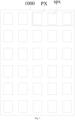
- a display panel may include a base substrate 1000, and a plurality of pixel units PX in a display region of the base substrate 1000.
- Each of the pixel units PX may include a plurality of sub-pixels spx.
- at least one of the plurality of sub-pixels spx may include a pixel driving circuit 0121 and a light emitting device 0120.
- the pixel driving circuit 0121 is provided with a transistor and a capacitor. An electric signal is generated by the interaction of the transistor and the capacitor, and the generated electric signal is input to a first electrode of the light emitting device 0120.
- a second electrode of the light emitting device 0120 is loaded with a corresponding voltage to drive the light emitting device 0120 to emit light.
- the pixel driving circuit 0121 may include a driving control circuit 0122, a first light emitting control circuit 0123, a second light emitting control circuit 0124, a voltage stabilizing circuit 0125, a data writing circuit 0126, a storage circuit 0127, a threshold compensation circuit 0128 and a reset circuit 0129.
- the driving control circuit 0122 may include a control end, a first end and a second end. Moreover, the driving control circuit 0122 is configured to provide a driving current for the light emitting device 0120 to drive the light emitting device 0120 to emit light.
- the first light emitting control circuit 0123 is connected to the first end of the driving control circuit 0122 and a first voltage end VDD. Moreover, the first light emitting control circuit 0123 is configured to realize the connection or disconnection between the driving control circuit 0122 and the first voltage end VDD.
- the second light emitting control circuit 0124 is electrically connected to the second end of the driving control circuit 0122 and the first electrode of the light emitting device 0120. Moreover, the second light emitting control circuit 0124 is configured to realize the connection or disconnection between the driving control circuit 0122 and the light emitting device 0120.
- the voltage stabilizing circuit 0125 is electrically connected to the control end of the driving control circuit 0122, the reset circuit 0129 and the threshold compensation circuit 0128 respectively, and the voltage stabilizing circuit 0125 is configured to connect the control end of the driving control circuit 0122 with the reset circuit 0129 to reset the control end of the driving control circuit 0122.
- the voltage stabilizing circuit 0125 is configured to connect the control end of the driving control circuit 0122 with the threshold compensation circuit 0128 so as to perform threshold compensation.
- the data writing circuit 0126 is electrically connected to the first end of the driving control circuit 0122. Moreover, the data writing circuit 0126 is configured to write a signal on a data line VD into the storage circuit 0127.
- the storage circuit 0127 is electrically connected to the control end of the driving control circuit 0122 and the first voltage end VDD. Moreover, the storage circuit 0127 is configured to store a data signal.
- the threshold compensation circuit 0128 is electrically connected to the voltage stabilizing circuit 0125 and the second end of the driving control circuit 0122. Moreover, the threshold compensation circuit 0128 is configured to perform threshold compensation on the driving control circuit 0122.
- the reset circuit 0129 is further electrically connected to the first electrode of the light emitting device 0120. Moreover, the reset circuit 0129 is configured to reset the first electrode of the light emitting device 0120 and provide a signal transmitted on an initialization line VINIT to the voltage stabilizing circuit 0125 so as to reset the control end of the driving control circuit 0122 when the control end of the driving control circuit 0122 is connected with the reset circuit 0129 by the voltage stabilizing circuit 0125.
- the light emitting device 0120 may be set as an electroluminescent diode such as at least one of an OLED and a QLED.
- the light emitting device 0120 may include a first electrode, a light emitting functional layer and a second electrode which are stacked.
- the first electrode may be an anode
- the second electrode may be a cathode.
- the light emitting functional layer may include a light emitting layer.
- the light emitting functional layer may further include film layers such as a hole injection layer, a hole transport layer, a light emitting layer, an electron transfer layer and an electron injection layer.
- the light emitting device 0120 may be designed and determined according to a demand of an actual application environment, which is not limited herein.
- the driving control circuit 0122 includes a driving transistor T1
- the control end of the driving control circuit 0122 includes a gate electrode of the driving transistor T1
- the first end of the driving control circuit 0122 includes a first electrode of the driving transistor T1
- the second end of the driving control circuit 0122 includes a second electrode of the driving transistor T1.
- the data writing circuit 0126 includes a data writing transistor T2.
- the storage circuit 0127 includes a storage capacitor CST.
- the threshold compensation circuit 0128 includes a threshold compensation transistor T3.
- the first light emitting control circuit 0123 includes a first light emitting control transistor T4.
- the second light emitting control circuit 0124 includes a second light emitting control transistor T5.
- the reset circuit 0129 includes an initialization transistor T6 and a second reset transistor T7.
- the voltage stabilizing circuit 0125 includes an oxide transistor T8.
- a first electrode of the data writing transistor T2 is electrically connected to the first electrode of the driving transistor T1
- a second electrode of the data writing transistor T2 is configured to be electrically connected to the data line VD so as to receive a data signal
- a gate electrode of the data writing transistor T2 is configured to be electrically connected to a third scanning line GA3 so as to receive a signal.
- a first electrode of the storage capacitor CST is electrically connected to a first power end VDD, and a second electrode of the storage capacitor CST is electrically connected to the gate electrode of the driving transistor T1.
- a first electrode of the threshold compensation transistor T3 is electrically connected to the second electrode of the driving transistor T1
- a second electrode of the threshold compensation transistor T3 is electrically connected to a first electrode of the oxide transistor T8
- a gate electrode of the threshold compensation transistor T3 is configured to be electrically connected to a third scanning line GA3 so as to receive a signal.
- a first electrode of the initialization transistor T6 is configured to be electrically connected to the initialization line VINIT so as to receive a reset signal
- a second electrode of the initialization transistor T6 is electrically connected to the first electrode of the oxide transistor T8
- a gate electrode of the initialization transistor T6 is configured to be electrically connected to a first scanning line GA1 so as to receive a signal.
- a first electrode of the second reset transistor T7 is configured to be electrically connected to the initialization line VINIT so as to receive a reset signal
- a second electrode of the second reset transistor T7 is electrically connected to the first electrode of the light emitting device 0120
- a gate electrode of the second reset transistor T7 is configured to be electrically connected to a fourth scanning line GA4 so as to receive a signal.
- a first electrode of the first light emitting control transistor T4 is electrically connected to the first power end VDD, a second electrode of the first light emitting control transistor T4 is electrically connected to the first electrode of the driving transistor T1, and a gate electrode of the first light emitting control transistor T4 is configured to be electrically connected to a light emitting control line EM so as to receive a light emitting control signal.
- a first electrode of the second light emitting control transistor T5 is electrically connected to the second electrode of the driving transistor T1
- a second electrode of the second light emitting control transistor T5 is electrically connected to the first electrode of the light emitting device 0120
- a gate electrode of the second light emitting control transistor T5 is configured to be electrically connected to the light emitting control line EM so as to receive a light emitting control signal.
- a second electrode of the oxide transistor T8 is electrically connected to the gate electrode of the driving transistor T1, and a gate electrode of the oxide transistor T8 is configured to be electrically connected to the first scanning line GA2 so as to receive a signal.
- the second electrode of the light emitting device 0120 is electrically connected to a second power end VSS.
- the first electrodes and the second electrodes of the above-mentioned transistors may be determined as source electrodes or drain electrodes according to actual application, which is not limited herein.
- one of the first power end VDD and the second power end VSS is a high-voltage end, and the other one is a low-voltage end.
- the first power end VDD is a voltage source so as to output a constant first voltage which is a positive voltage
- the second power end VSS may be a voltage source so as to output a constant second voltage which is a negative voltage.
- the second power end VSS may be grounded.
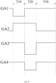
- a timing diagram of signals corresponding to the pixel driving circuit as shown in Fig. 2A is shown in Fig. 2b .
- a working process of the pixel driving circuit is divided into three stages: stage T10, stage T20 and stage T30, ga1 represents a signal transmitted on a first scanning line GA1, ga2 represents a signal transmitted on a second scanning line GA2, ga3 represents a signal transmitted on a third scanning line GA3, ga4 represents a signal transmitted on a fourth scanning line GA4, and em represents a signal transmitted on a light emitting control line EM.
- the signal ga1 controls the initialization transistor T6 to be turned on, and the signal ga2 controls the oxide transistor T8 to be turned on, so that the signal transmitted on the initialization line VINIT may be provided to the gate electrode of the driving transistor T1 to reset the gate electrode of the driving transistor T1.
- the signal ga4 controls the second reset transistor T7 to be turned on, so that the signal transmitted on the initialization line VINIT may be provided to the first electrode of the light emitting device 0120 to reset the first electrode of the light emitting device 0120.
- the signal ga3 controls both the data writing transistor T2 and the threshold compensation transistor T3 to be turned off.
- the signal em controls both the first light emitting control transistor T4 and the second light emitting control transistor T5 to be turned off.
- the signal ga3 controls both the data writing transistor T2 and the threshold compensation transistor T3 to be turned on.
- the signal ga2 controls the oxide transistor T8 to be turned on, so that the data signal transmitted on the data line VD may charge the gate electrode of the driving transistor T1 to change a voltage of the gate electrode of the driving transistor T1 to be Vdata+Vth, Vth represents a threshold voltage of the driving transistor T1, and Vdata represents a voltage of the data signal.
- the signal ga1 controls the initialization transistor T6 to be turned off, and the signal ga4 controls the second reset transistor T7 to be turned off.
- the signal em controls both the first light emitting control transistor T4 and the second light emitting control transistor T5 to be turned off.
- the signal em controls both the first light emitting control transistor T4 and the second light emitting control transistor T5 to be turned on.
- the turned-on first light emitting control transistor T4 provides a voltage V vdd of the first power end VDD to the first electrode of the driving transistor T1, so that a voltage of the first electrode of the driving transistor T1 is V vdd .
- the driving transistor T1 generates a driving current according to the voltage Vdata+Vth of the gate electrode and the voltage V vdd of the first electrode of the driving transistor T1.
- the driving current is provided to the light emitting device 0120 by the turned-on second light emitting control transistor T5 so as to drive the light emitting device 0120 to emit light.
- the signal ga1 controls the initialization transistor T6 to be turned off, and the signal ga4 controls the second reset transistor T7 to be turned off.
- the signal ga3 controls both the data writing transistor T2 and the threshold compensation transistor T3 to be turned off.
- the signal ga2 controls the oxide transistor T8 to be turned off.
- FIG. 2C another timing diagram of signals corresponding to the pixel driving circuit as shown in Fig. 2A is shown in Fig. 2C .
- a working process of the pixel driving circuit is divided into three stages: stage T10, stage T20 and stage T30, ga1 represents a signal transmitted on a first scanning line GA1, ga2 represents a signal transmitted on a second scanning line GA2, ga3 represents a signal transmitted on a third scanning line GA3, ga4 represents a signal transmitted on a fourth scanning line GA4, and em represents a signal transmitted on a light emitting control line EM.
- the signal ga4 controls the second reset transistor T7 to be turned off
- the rest working process may refer to the above-mentioned embodiment, which is not described in detail herein.
- the signal ga4 controls the second reset transistor T7 to be turned on, so that the signal transmitted on the initialization line VINIT may be provided to the first electrode of the light emitting device 0120 to reset the first electrode of the light emitting device 0120.
- the rest working process may refer to the above-mentioned embodiment, which is not described in detail herein.
- the working process at this stage may refer to the above-mentioned embodiment, which is not described in detail herein.
- a further timing diagram of signals corresponding to the pixel driving circuit as shown in Fig. 2A is shown in Fig. 2D .
- a working process of the pixel driving circuit is divided into four stages: stage T10, stage T20, stage T30 and stage T40, ga1 represents a signal transmitted on a first scanning line GA1, ga2 represents a signal transmitted on a second scanning line GA2, ga3 represents a signal transmitted on a third scanning line GA3, ga4 represents a signal transmitted on a fourth scanning line GA4, and em represents a signal transmitted on a light emitting control line EM.
- the signal ga4 controls the second reset transistor T7 to be turned on, so that the signal transmitted on the initialization line VINIT is provided to the first electrode of the light emitting device 0120 to reset the first electrode of the light emitting device 0120.
- the signal ga1 controls the initialization transistor T6 to be turned off
- the signal ga3 controls both the data writing transistor T2 and the threshold compensation transistor T3 to be turned off.
- the signal em controls both the first light emitting control transistor T4 and the second light emitting control transistor T5 to be turned off.
- the signal ga2 controls the oxide transistor T8 to be turned off.
- the signal ga1 controls the initialization transistor T6 to be turned on, and the signal ga2 controls the oxide transistor T8 to be turned on, so that the signal transmitted on the initialization line VINIT may be provided to the gate electrode of the driving transistor T1 to reset the gate electrode of the driving transistor T1.
- the signal ga4 controls the second reset transistor T7 to be turned off, and the signal ga3 controls both the data writing transistor T2 and the threshold compensation transistor T3 to be turned off.
- the signal em controls both the first light emitting control transistor T4 and the second light emitting control transistor T5 to be turned off.
- the signal ga3 controls both the data writing transistor T2 and the threshold compensation transistor T3 to be turned on.
- the signal ga2 controls the oxide transistor T8 to be turned on, so that the data signal transmitted on the data line VD may charge the gate electrode of the driving transistor T1 to change a voltage of the gate electrode of the driving transistor T1 to be Vdata+Vth, Vth represents a threshold voltage of the driving transistor T1, and Vdata represents a voltage of the data signal.
- the signal ga1 controls the initialization transistor T6 to be turned off, and the signal ga4 controls the second reset transistor T7 to be turned off.
- the signal em controls both the first light emitting control transistor T4 and the second light emitting control transistor T5 to be turned off.
- the signal em controls both the first light emitting control transistor T4 and the second light emitting control transistor T5 to be turned on.
- the turned-on first light emitting control transistor T4 provides a voltage V vdd of the first power end VDD to the first electrode of the driving transistor T1, so that a voltage of the first electrode of the driving transistor T1 is V vdd .
- the driving transistor T1 generates a driving current according to the voltage Vdata+Vth of the gate electrode and the voltage V vdd of the first electrode of the driving transistor T1.
- the driving current is provided to the light emitting device 0120 by the turned-on second light emitting control transistor T5 so as to drive the light emitting device 0120 to emit light.
- the signal ga1 controls the initialization transistor T6 to be turned off, and the signal ga4 controls the second reset transistor T7 to be turned off.
- the signal ga3 controls both the data writing transistor T2 and the threshold compensation transistor T3 to be turned off.
- the signal ga2 controls the oxide transistor T8 to be turned off.
- a yet further timing diagram of signals corresponding to the pixel driving circuit as shown in Fig. 2A is shown in Fig. 2E .
- a working process of the pixel driving circuit is divided into four stages: stage T10, stage T20, stage T30 and stage T40, ga1 represents a signal transmitted on a first scanning line GA1, ga2 represents a signal transmitted on a second scanning line GA2, ga3 represents a signal transmitted on a third scanning line GA3, ga4 represents a signal transmitted on a fourth scanning line GA4, and em represents a signal transmitted on a light emitting control line EM.
- the signal ga1 controls the initialization transistor T6 to be turned on, and the signal ga2 controls the oxide transistor T8 to be turned on, so that the signal transmitted on the initialization line VINIT may be provided to the gate electrode of the driving transistor T1 to reset the gate electrode of the driving transistor T1.
- the signal ga4 controls the second reset transistor T7 to be turned off, and the signal ga3 controls both the data writing transistor T2 and the threshold compensation transistor T3 to be turned off.
- the signal em controls both the first light emitting control transistor T4 and the second light emitting control transistor T5 to be turned off.
- the signal ga4 controls the second reset transistor T7 to be turned on, so that the signal transmitted on the initialization line VINIT may be provided to the first electrode of the light emitting device 0120 to reset the first electrode of the light emitting device 0120.
- the signal ga1 controls the initialization transistor T6 to be turned off
- the signal ga3 controls both the data writing transistor T2 and the threshold compensation transistor T3 to be turned off.
- the signal em controls both the first light emitting control transistor T4 and the second light emitting control transistor T5 to be turned off.
- the signal ga3 controls both the data writing transistor T2 and the threshold compensation transistor T3 to be turned on.
- the signal ga2 controls the oxide transistor T8 to be turned on, so that the data signal transmitted on the data line VD may charge the gate electrode of the driving transistor T1 to change a voltage of the gate electrode of the driving transistor T1 to be Vdata+Vth, Vth represents a threshold voltage of the driving transistor T1, and Vdata represents a voltage of the data signal.
- the signal ga1 controls the initialization transistor T6 to be turned off, and the signal ga4 controls the second reset transistor T7 to be turned off.
- the signal em controls both the first light emitting control transistor T4 and the second light emitting control transistor T5 to be turned off.
- the signal em controls both the first light emitting control transistor T4 and the second light emitting control transistor T5 to be turned on.
- the turned-on first light emitting control transistor T4 provides a voltage V vdd of the first power end VDD to the first electrode of the driving transistor T1, so that a voltage of the first electrode of the driving transistor T1 is V vdd .
- the driving transistor T1 generates a driving current according to the voltage Vdata+Vth of the gate electrode and the voltage V vdd of the first electrode of the driving transistor T1.
- the driving current is provided to the light emitting device 0120 by the turned-on second light emitting control transistor T5 so as to drive the light emitting device 0120 to emit light.
- the signal ga1 controls the initialization transistor T6 to be turned off, and the signal ga4 controls the second reset transistor T7 to be turned off.
- the signal ga3 controls both the data writing transistor T2 and the threshold compensation transistor T3 to be turned off.
- the signal ga2 controls the oxide transistor T8 to be turned off.
- the pixel driving circuit in the sub-pixel may also be of a structure including another number of transistors in addition to the structure as shown in Fig. 2A , which is not limited herein.
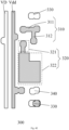
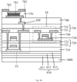
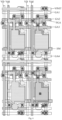
- Fig. 3 is a schematic structural diagram showing layout of a pixel driving circuit provided by embodiments of the disclosure.
- Fig. 4A to Fig. 4F are schematic diagrams of each layer of the pixel driving circuit provided by embodiments of the disclosure. Examples shown in Fig. 3 to Fig. 4F are described with a pixel driving circuit of one sub-pixel spx as an example.
- Fig. 3 to Fig. 4F further show a first scanning line GA1, a second scanning line GA2, a third scanning line GA3, a fourth scanning line GA4, an initialization line VINIT, a light emitting control line EM, a data line VD and a first power line part Vdd which are electrically connected to a pixel driving circuit 0121.
- the first power line part Vdd is configured to input a driving voltage (that is, a first voltage) to the first power end VDD.
- a plurality of data lines VD may be arranged in a first direction F1.
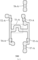
- a silicon semiconductor layer 500 of the pixel driving circuit 0121 is shown.
- the silicon semiconductor layer 500 may be formed by patterning an amorphous silicon material or an LTPS (Low Temperature Poly-Silicon) material.
- the silicon semiconductor layer 500 may be used for manufacturing active silicon layers of the driving transistor T1, the data writing transistor T2, the threshold compensation transistor T3, the first light emitting control transistor T4, the second light emitting control transistor T5, the initialization transistor T6 and the second reset transistor T7.
- each of the active silicon layer may include a first region, a second region and a first channel region between the first region and the second region.
- each of the above-mentioned first region and second region may be a conductor region formed by a region, in which n-type impurities or p-type impurities are doped, in the silicon semiconductor layer 500. Therefore, the first region and the second region may be used as a source electrode region and a drain electrode region of the active silicon layer for performing an electrical connection.
- the active silicon layer of the initialization transistor T6 may extend approximately in a straight line in a second direction F2.
- an extension direction of the active silicon layer of the initialization transistor T6 is approximately parallel to the second direction F2.
- the extension direction of the active silicon layer of the initialization transistor T6 may not be completely parallel to the second direction, it is possible to generate some deviations, and therefore, as long as the above-mentioned extension direction of the active silicon layer of the initialization transistor T6 and the second direction shall approximately meet parallel conditions, it shall fall within the protective scope of the disclosure.
- the above-mentioned parallel may be allowed within an error allowable range.
- the active silicon layer of the threshold compensation transistor T3 may extend approximately in a straight line in the second direction F2.
- an extension direction of the active silicon layer of the threshold compensation transistor T3 is approximately parallel to the second direction F2.
- the extension direction of the active silicon layer of the threshold compensation transistor T3 may not be completely parallel to the second direction, it is possible to generate some deviations, and therefore, as long as the above-mentioned extension direction of the active silicon layer of the threshold compensation transistor T3 and the second direction approximately meet parallel conditions, it shall fall within the protective scope of the disclosure.
- the above-mentioned parallel may be allowed within an error allowable range.
- a first insulating layer 710 is formed on the above-mentioned silicon semiconductor layer 500 and is used for protecting the above-mentioned silicon semiconductor layer 500.
- a first conducting layer 100 of the pixel driving circuit 0121 is shown. The first conducting layer 100 is arranged at a side, facing away from the base substrate 1000, of the first insulating layer 710, thereby being insulated from the silicon semiconductor layer 500.
- the first conducting layer 100 may include a plurality of scanning lines spaced from one another, a plurality of light emitting control lines EM spaced from one another as well as a gate electrode CC2a of the driving transistor T1, a gate electrode T2-G of the data writing transistor T2, a gate electrode T3-G of the threshold compensation transistor T3, a gate electrode T4-G of the first light emitting control transistor T4, a gate electrode T5-G of the second light emitting control transistor T5, a gate electrode T6-G of the initialization transistor T6, a gate electrode T7-G of the second reset transistor T7 and a first gate electrode T8-G1 of the oxide transistor T8.
- the plurality of scanning lines may include, for example, a plurality of first scanning lines GA1, a plurality of second scanning lines GA2, a plurality of third scanning lines GA3 and a plurality of fourth scanning lines GA4 spaced from one another.
- a row of sub-pixels corresponds to one of the first scanning lines GA1, one of the second scanning lines GA2, one of the third scanning lines GA3, one of the fourth scanning lines GA4 and one of the light emitting control lines EM.
- the gate electrode T2-G of the data writing transistor T2 may be a first part, overlapped with the silicon semiconductor layer 500, of the third scanning line GA3.
- An orthographic projection of the third scanning line GA3 on the base substrate 1000 is overlapped with an orthographic projection of the first channel region T3-A of the active silicon layer of the threshold compensation transistor T3 on the base substrate 1000 to form a third overlapping region, and a part, in the third overlapping region, of the third scanning line GA3 is the gate electrode T3-G of the threshold compensation transistor T3, that is, the gate electrode T3-G of the threshold compensation transistor T3 may be a second part, overlapped with the silicon semiconductor layer 500, of the third scanning line GA3.
- An orthographic projection of the light emitting control line EM on the base substrate 1000 is overlapped with the first channel region T4-A of the active silicon layer of the first light emitting control transistor T4 to form a fourth overlapping region, and a part, in the fourth overlapping region, of the light emitting control line EM is the gate electrode T4-G of the first light emitting control transistor T4, that is, the gate electrode T4-G of the first light emitting control transistor T4 may be a first part, overlapped with the silicon semiconductor layer 500, of the light emitting control line EM.
- An orthographic projection of the light emitting control line EM on the base substrate 1000 is overlapped with the first channel region T5-A of the active silicon layer of the second light emitting control transistor T5 to form a fifth overlapping region, and a part, in the fifth overlapping region, of the light emitting control line EM is the gate electrode T5-G of the second light emitting control transistor T5, that is, the gate electrode T5-G of the second light emitting control transistor T5 may be a second part, overlapped with the silicon semiconductor layer 500, of the light emitting control line EM.
- an orthographic projection of the first scanning line GA1 on the base substrate 1000 is overlapped with an orthographic projection of the first channel region T6-A of the active silicon layer of the initialization transistor T6 on the base substrate 1000 to form a first overlapping region, and a part, in the first overlapping region, of the first scanning line GA1 is the gate electrode T6-G of the initialization transistor T6, that is, the gate electrode T6-G of the initialization transistor T6 may be a first part, overlapped with the silicon semiconductor layer 500, of the first scanning line GA1, and the gate electrode T7-G of the second reset transistor T7 may be a first part, overlapped with the silicon semiconductor layer 500, of the fourth scanning line GA4.
- the first gate electrode T8-G1 of the oxide transistor T8 may be a first part, overlapped with the silicon semiconductor layer 500, of the second scanning line GA2.
- the gate electrode CC2a of the driving transistor T1 may be set as an electrode plate of the storage capacitor CST.
- the gate electrode CC2a of the driving transistor T1 and one electrode plate of the storage capacitor CST are of an integrated structure.
- an orthographic projection of the second scanning line GA2 on the base substrate 1000 is overlapped with an orthographic projection of the second channel region T8-A of an active oxide layer of the oxide transistor T8 on the base substrate 1000 to form a second overlapping region, and a part, in the second overlapping region, of the second scanning line GA2 is the first gate electrode T8-G1 of the oxide transistor T8.
- the first scanning line GA1, the second scanning line GA2, the third scanning line GA3, the light emitting control line EM and the fourth scanning line GA4 extend in the first direction F1.
- the first scanning line GA1, the second scanning line GA2, the third scanning line GA3, the light emitting control line EM and the fourth scanning line GA4 are arranged in the second direction F2.
- the orthographic projection of the second scanning line GA2 on the base substrate 1000 is located between the orthographic projection of the first scanning line GA1 on the base substrate 1000 and the orthographic projection of the third scanning line GA3 on the base substrate 1000.
- the orthographic projection of the third scanning line GA3 on the base substrate 1000 is located between the orthographic projection of the second scanning line GA2 on the base substrate 1000 and the orthographic projection of the light emitting control line EM on the base substrate 1000.
- An orthographic projection of the fourth scanning line GA4 on the base substrate 1000 is at a side, facing away from the orthographic projection of the third scanning line GA3 on the base substrate 1000, of the orthographic projection of the light emitting control line EM on the base substrate 1000.
- an orthographic projection of the active oxide layer of the oxide transistor T8 on the base substrate 1000 is located between the orthographic projection of the first scanning line GA1 on the base substrate 1000 and the orthographic projection of the third scanning line GA3 on the base substrate 1000, and the orthographic projection of the second scanning line GA2 on the base substrate 1000 is respectively not overlapped with an orthographic projection of the active silicon layer of the threshold compensation transistor T3 on the base substrate 1000 and an orthographic projection of the active silicon layer of the initialization transistor T6 on the base substrate 1000.
- the orthographic projection of the second scanning line GA2 on the base substrate 1000 is partially overlapped with an orthographic projection of the first region of the active silicon layer of the threshold compensation transistor T3 on the base substrate 1000.
- the orthographic projection of the second scanning line GA2 on the base substrate 1000 may also partially overlapped with an orthographic projection of the second region of the active silicon layer of the initialization transistor T6 on the base substrate 1000.
- these setting ways may be designed and determined according to a demand of actual application, which is not limited herein.
- an orthographic projection of the light emitting control line EM on the base substrate 1000 is at a side, facing away from the orthographic projection of the second scanning line GA2 on the base substrate 1000, of the orthographic projection of the third scanning line GA3 on the base substrate 1000.
- the orthographic projection of the fourth scanning line GA4 on the base substrate 1000 is at the side, facing away from the orthographic projection of the second scanning line GA2 on the base substrate 1000, of the orthographic projection of the light emitting control line EM on the base substrate 1000.
- Both orthographic projections of the active silicon layer and the gate electrode of the driving transistor T1 on the base substrate 1000 are between the orthographic projection of the light emitting control line EM on the base substrate 1000 and the orthographic projection of the third scanning line GA3 on the base substrate 1000.
- an orthographic projection of the gate electrode CC2a of the driving transistor T1 on the base substrate 1000 is between the orthographic projection of the third scanning line GA3 on the base substrate 1000 and the orthographic projection of the light emitting control line EM on the base substrate 1000.
- the gate electrode T2-G of the data writing transistor T2, the gate electrode T3-G of the threshold compensation transistor T3, the gate electrode T6-G of the initialization transistor T6 and the first gate electrode T8-G1 of the oxide transistor T8 are located at the side, facing away from the light emitting control line EM, of the gate electrode of the driving transistor T1, and the gate electrode T7-G of the second reset transistor T7, the gate electrode T4-G of the first light emitting control transistor T4 and the gate electrode T5-G of the second light emitting control transistor T5 are located at the side, facing away from the first scanning line GA1, of the gate electrode of the driving transistor T1.
- both the gate electrode T2-G of the data writing transistor T2 and the gate electrode T4-G of the first light emitting control transistor T4 are located at a third side of the gate electrode of the driving transistor T1
- the gate electrode T3-G of the threshold compensation transistor T3 the gate electrode T5-G of the second light emitting control transistor T5
- the gate electrode T6-G of the initialization transistor T6 and the gate electrode T7-G of the second reset transistor T7 are located at a fourth side of the gate electrode of the driving transistor T1.
- the third side and the fourth side of the gate electrode of the driving transistor T1 are two sides, opposite to each other in the first direction F1, of the gate electrode of the driving transistor T1.
- the first gate electrode T8-G1 of the oxide transistor T8 and the gate electrode of the driving transistor T1 are arranged, in the first direction F1, in a straight line.
- the center of the first gate electrode T8-G1 of the oxide transistor T8 and the center of the gate electrode of the driving transistor T1 are arranged, in the first direction F1, in a straight line.
- a second insulating layer 720 is formed on the above-mentioned first conducting layer 100 and is used for protecting the above-mentioned first conducting layer 100.
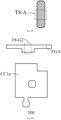
- an oxide semiconductor layer 600 of the pixel driving circuit 0121 is shown.
- the oxide semiconductor layer 600 is arranged at a side, facing away from the base substrate 1000, of the second insulating layer 720.
- the oxide semiconductor layer 600 may be formed by patterning an oxide semiconductor material.
- the oxide semiconductor material may be, for example, IGZO (Indium Gallium Zinc Oxide).
- the oxide semiconductor layer 600 may include the active oxide layer of the oxide transistor T8.
- the active oxide layer is provided with a third region, a fourth region and a second channel region T8-Abetween the third region and the fourth region.
- Fig. 4C shows the second channel region T8-A of the oxide transistor T8.
- each of the third region and the fourth region may be a conductor region formed by a region, in which n-type impurities or p-type impurities are doped, in the oxide semiconductor layer 600. Therefore, the third region and the fourth region may be used as a source electrode region and a drain electrode region of the active oxide layer for performing an electrical connection.
- the active oxide layer of the oxide transistor T8 extends approximately in a straight line in the second direction F2.
- an extension direction of the active oxide layer of the oxide transistor T8 is approximately parallel to the second direction F2.
- the extension direction of the active oxide layer of the oxide transistor T8 may not be completely parallel to the second direction, it is possible to generate some deviations, and therefore, as long as the extension direction of the active oxide layer of the above-mentioned oxide transistor T8 and the second direction approximately meet parallel directions, it shall fall within the protective scope of the disclosure.
- the above-mentioned parallel may be allowed within an error allowable range.
- a third insulating layer 730 is formed on the above-mentioned oxide semiconductor layer 600 and is used for protecting the above-mentioned oxide semiconductor layer 600.
- a second conducting layer 200 of the pixel driving circuit 0121 is shown.
- the second conducting layer 200 is arranged at a side, facing away from the base substrate 1000, of the third insulating layer 730.
- the second conducting layer 200 may include a plurality of auxiliary scanning lines FGA spaced from one another and a storage conducting part CC1a spaced from the auxiliary scanning lines FGA.
- an orthographic projection of the storage conducting part CC1a on the base substrate 1000 is at least partially overlapped with the orthographic projection of the gate electrode CC2a of the driving transistor T1 on the base substrate 1000 to form a storage capacitor CST.
- a row of sub-pixels corresponds to one of the auxiliary scanning lines FGA.
- An orthographic projection of the auxiliary scanning line FGA on the base substrate 1000 is overlapped with an orthographic projection of the second channel region T8-A of the active oxide layer of the oxide transistor T8 on the base substrate 1000 to form a sixth overlapping region.
- the second gate electrode T8-G2 of the oxide transistor T8 may be a first part, overlapped with the second channel region T8-A, of the auxiliary scanning line FGA.
- the oxide transistor T8 is a double-gate transistor.
- the part, in the second overlapping region, of the second scanning line GA2 is a first gate electrode T8-G1 of the oxide transistor T8, and the part, in the sixth overlapping region, of the auxiliary scanning line FGA is a second gate electrode T8-G2 of the oxide transistor T8.
- the orthographic projection of the auxiliary scanning line FGA on the base substrate 1000 is overlapped with the orthographic projection of the second scanning line GA2 on the base substrate 1000, and the auxiliary scanning line FGA and the second scanning line GA2 in the same sub-pixel are electrically connected.
- the auxiliary scanning line FGA and the second scanning line GA2 in the same sub-pixel may be electrically connected on an edge of an effective display region through a via hole.
- the auxiliary scanning line FGA and the second scanning line GA2 in the same sub-pixel may be electrically connected in the display region through the via hole.
- a fourth insulating layer 740 is formed on the above-mentioned second conducting layer 200 and is used for protecting the above-mentioned second conducting layer 200.
- a third conducting layer 300 of the pixel driving circuit 0121 is shown. The third conducting layer 300 is arranged at a side, facing away from the base substrate 1000, of the fourth insulating layer 740.
- the third conducting layer 300 may include a plurality of data lines VD, a plurality of first power line parts Vdd, a plurality of first connection parts 310, a plurality of second connection parts 320, a plurality of third connection parts 330 and a plurality of fourth connection parts 340 spaced from one another.
- the data lines VD, the first power line parts Vdd, the first connection parts 310, the second connection parts 320, the third connection parts 330 and the fourth connection parts 340 are spaced from one another.
- the data lines VD and the first power line parts Vdd are arranged in a first direction, and the first data line parts VD and the power lines Vdd extend in a second direction.
- One of the first connection parts 310, one of the second connection parts 320, one of the third connection parts 330 and one of the fourth connection parts 340 are arranged in one sub-pixel.
- a column of sub-pixels corresponds to one of the first data line parts Vdd and one of the data lines VD.
- an orthographic projection of the first data line part Vdd on the base substrate 1000 is located between an orthographic projection of the data line VD on the base substrate 1000 and an orthographic projection of the second connection part 320 on the base substrate 1000.
- both the orthographic projection of the active silicon layer of the initialization transistor T6 on the base substrate 1000 and the orthographic projection of the active silicon layer of the threshold compensation transistor T3 on the base substrate 1000 are located at a side, facing away from the orthographic projection of the data line VD on the base substrate 1000, of the orthographic projection of the active oxide layer of the oxide transistor T8 on the base substrate 1000.
- the orthographic projection of the active silicon layer of the initialization transistor T6 on the base substrate 1000 is a first orthographic projection
- the orthographic projection of the active silicon layer of the threshold compensation transistor T3 on the base substrate 1000 is a second orthographic projection
- the orthographic projection of the active oxide layer of the oxide transistor T8 on the base substrate 1000 is a third orthographic projection
- the orthographic projection of the data line VD on the base substrate 1000 is a fourth orthographic projection
- the first orthographic projection is located at a side, facing away from the fourth orthographic projection, of the third orthographic projection
- the second orthographic projection is also located at the side, facing away from the fourth orthographic projection, of the third orthographic projection, so that both the first orthographic projection and the second orthographic projection may be located at the side, facing away from the fourth orthographic projection, of the third orthographic projection.
- a fifth insulating layer 750 is formed on the above-mentioned third conducting layer 300 and is used for protecting the above-mentioned third conducting layer 300.
- a fourth conducting layer 400 of the pixel driving circuit 0121 is shown.
- the fourth conducting layer 400 is arranged at a side, facing away from the base substrate 1000, of the fifth insulating layer 750.
- the fourth conducting layer 400 may include a plurality of initialization lines VINIT spaced from one another, a plurality of second power line parts 410 spaced from one another and a plurality of switching parts 420.
- the initialization lines VINIT, the second power line parts 410 and the switching parts 420 are spaced from one another.
- a sub-pixel is provided with one second power line part 410 and one switching part 420.
- a row of sub-pixels corresponds to one of the initialization lines VINIT.
- an orthographic projection of the initialization line VINIT on the base substrate 1000 is located at the side, facing away from the orthographic projection of the second scanning line GA2 on the base substrate 1000, of the orthographic projection of the first scanning line GA1 on the base substrate 1000.
- Fig. 5A is a sectional view in AA' direction in the schematic structural diagram showing the layout of the pixel driving circuit in Fig. 3 .
- Fig. 5B is a sectional view in BB' direction in the schematic structural diagram showing the layout in Fig. 3 .
- Fig. 5C is a sectional view in CC' direction in the schematic structural diagram showing the layout in Fig. 3 .
- Fig. 5D is a partial sectional view in the schematic structural diagram showing the layout in Fig. 3 .
- Fig. 6 is a schematic structural diagram showing layout of pixel driving circuits in two rows and two columns of sub-pixels in embodiments of the disclosure.
- Fig. 5D only shows the oxide transistor T8 and the second light emitting control transistor T5 in the pixel driving circuit 0121.
- a first buffer layer 810 is arranged between the silicon semiconductor layer 500 and the base substrate 1000.
- the first insulating layer 710 is arranged between the silicon semiconductor layer 500 and the first conducting layer 100
- the second insulating layer 720 is arranged between the first conducting layer 100 and the oxide semiconductor layer 600.
- the third insulating layer 730 is arranged between the oxide semiconductor layer 600 and the second conducting layer 200.
- the fourth insulating layer 740 is arranged between the second conducting layer 200 and the third conducting layer 300.
- the fifth insulating layer 750 is arranged between the third conducting layer 300 and the fourth conducting layer 400. Further, the side, facing away from the base substrate 1000, of the fourth conducting layer 400 is provided with a first planarization layer 760.
- a side, facing away from the base substrate 1000, of the first planarization layer 760 is provided with a first electrode layer.
- a side, facing away from the base substrate 1000, of the first electrode layer is sequentially provided with a pixel defining layer 770, a light emitting functional layer 781 and a second electrode layer 782.
- the first electrode layer may include a plurality of first electrodes 783 spaced from one another, and the first electrodes 783 are electrically connected to the switching parts 420 through via holes penetrating through the first planarization layer 760. It should be noted that the via holes penetrating through the first planarization layer 760 are not shown in Fig. 5A and Fig. 5B .
- the above-mentioned insulating layers may be made of organic material or inorganic material (such as SiOx and SiNx), which is not limited herein.
- the first buffer layer 810 may include a first sub-buffer layer 811, a second sub-buffer layer 812 and a third sub-buffer layer 813 which are stacked.
- the first sub-buffer layer 811 is between the base substrate 1000 and the second sub-buffer layer 812
- the third sub-buffer layer 813 is between the second sub-buffer layer 812 and the silicon semiconductor layer 500.
- at least one of the first sub-buffer layer 811, the second sub-buffer layer 812 and the third sub-buffer layer 813 may be set to be made of the inorganic material or the organic material.
- the first sub-buffer layer 811 is set to be made of the organic material such as PI (Polyimide), and the second sub-buffer layer 812 and the third sub-buffer layer 813 may be set to be made of the inorganic material such as SiOx and SiNx.
- PI Polyimide
- the second sub-buffer layer 812 and the third sub-buffer layer 813 may be set to be made of the inorganic material such as SiOx and SiNx.
- the second insulating layer 720 may include a second sub-insulating layer 721 and a second buffer layer 722 which are stacked.
- the second sub-insulating layer 721 is located between the first conducting layer 100 and the second buffer layer 722, and the second buffer layer 722 is located between the second sub-insulating layer 721 and the oxide semiconductor layer 600.
- the second sub-insulating layer 721 may be set to be made of an inorganic material such as SiNx and SiOx, and SiNx may be adopted during specific implementation.
- the second buffer layer 722 may be set to be made of an inorganic material such as SiNx and SiOx, and SiOx may be adopted during specific implementation.
- the fifth insulating layer 750 may include a PVX (Passivation) layer 751 and a second planarization layer 752 which are stacked.
- the PVX layer 751 is located between the third conducting layer 300 and the second planarization layer 752, and the second planarization layer 752 is located between the PVX layer 751 and the fourth conducting layer 400.
- the PVX layer 751 may be made of an inorganic material such as SiOx and SiNx, and the second planarization layer 752 may be made of an organic material.
- the sub-pixel spx may include first connection through holes 511, 512, 513, 514, 515 and 516.
- the sub-pixel spx may include a second connection through hole 521.
- the sub-pixel spx may include third connection through holes 531 and 532.
- the sub-pixel spx may include a fourth connection through hole 541.
- the sub-pixel spx may include fifth connection through holes 551, 552 and 553.
- the first connection through holes 511, 512, 513, 514, 515 and 516 penetrate through the first insulating layer 710, the second insulating layer 720, the third insulating layer 730 and the fourth insulating layer 740.
- the second connection through hole 521 penetrates through the second insulating layer 720, the third insulating layer 730 and the fourth insulating layer 740.
- the third connection through holes 531 and 532 penetrate through the third insulating layer 730 and the fourth insulating layer 740.
- the fourth connection through hole 541 penetrates through the fourth insulating layer 740.
- the fifth connection through holes 551, 552 and 553 penetrate through the fifth insulating layer 750.
- the above-mentioned connection through holes are disposed at intervals.
- the third connection through hole 531 is used as a first via hole
- the first connection through hole 513 is used as a second via hole
- the first connection through hole 512 is used as a third via hole.
- the data line VD is electrically connected to the first region of the data writing transistor T2 in the silicon semiconductor layer 500 through at least one first connection through hole 511.
- the first power line part Vdd is electrically connected to a first region T4-S of the first light emitting control transistor T4 in the silicon semiconductor layer 500 through at least one first connection through hole 515 (that is, a fourth via hole).
- the first power line part Vdd is further electrically connected to the storage conducting part CC1a through at least one fourth connection through hole 541 (that is, an eighth via hole).
- One end of the third connection part 330 is electrically connected to a first region T6-S of the initialization transistor T6 in the silicon semiconductor layer 500 through at least one first connection through hole 514 (that is, a tenth via hole).
- the other end of the third connection part 330 is electrically connected to the initialization line VINIT through at least one fifth connection through hole 552 (that is, a ninth via hole).
- the first connection part 310 is electrically connected to a second region T6-D of the initialization transistor T6 in the silicon semiconductor layer 500 through at least one first connection through hole 513 (that is, the second via hole).
- the first connection part 310 is further electrically connected to a second region T3-D of the threshold compensation transistor T3 in the silicon semiconductor layer 500 through at least one first connection through hole 512 (that is, the third via hole).
- the first connection part 310 is further electrically connected to a third region T8-S of the oxide transistor T8 in the oxide semiconductor layer 600 through at least one third connection through hole 531 (that is, the first via hole).
- One end of the fourth connection part 340 is electrically connected to each of a second region T5-D of the second light emitting control transistor T5 in the silicon semiconductor layer 500 and a second region T7-D of the second reset transistor T7 in the silicon semiconductor layer 500 through at least one first connection through hole 516 (that is, a fifth via hole).
- the other end of the fourth connection part 340 is electrically connected to the switching part 420 through at least one fifth connection through hole 553.
- One end of the second connection part 320 is electrically connected to a fourth region T8-D of the oxide transistor T8 in the oxide semiconductor layer 600 through at least one third connection through hole 532 (that is, a sixth via hole).
- the other end of the second connection part 320 is electrically connected to the gate electrode CC2a of the driving transistor T1 through at least one second connection through hole 521 (that is, a seventh via hole).
- the second power line part 410 is electrically connected to the first power line part Vdd through at least one fifth connection through hole 551.
- the number of each of the first connection through holes 511, 512, 513, 514, 515 and 516 in the sub-pixel may be set to be one or two or more. In actual application, the number may be designed and determined according to a demand of an actual application environment, which is not limited herein.
- the number of the second connection through hole 521 in the sub-pixel may be set to be one or two or more. In actual application, the number may be designed and determined according to a demand of an actual application environment, which is not limited herein.
- the number of each of the third connection through holes 531 and 532 in the sub-pixel may be set to be one or two or more. In actual application, the number may be designed and determined according to a demand of an actual application environment, which is not limited herein.
- the number of the fourth connection through hole 541 in the sub-pixel may be set to be one or two or more. In actual application, the number may be designed and determined according to a demand of an actual application environment, which is not limited herein.
- the number of each of the fifth connection through holes 551, 552 and 553 in the sub-pixel may be set to be one or two or more. In actual application, the number may be designed and determined according to a demand of an actual application environment, which is not limited herein.
- a positional arrangement relationship among the transistors in each sub-pixel spx is not limited to examples as shown in Fig. 3 to Fig. 4F , and positions of the above-mentioned transistors may be set specifically according to a demand of actual application.
- first direction F1 may be a row direction of the sub-pixels
- second direction F2 may be a column direction of the sub-pixels
- first direction F1 may be the column direction of the sub-pixels
- second direction F2 may be the row direction of the sub-pixels.
- first direction F1 and the second direction F2 may be set according to a demand of actual application, which is not limited herein.
- the first region T6-S of the active silicon layer of the initialization transistor T6 is used as the first electrode of the initialization transistor T6, and the second region T6-D of the active silicon layer of the initialization transistor T6 is used as the second electrode of the initialization transistor T6.
- the third region T8-S of the active oxide layer of the oxide transistor T8 is used as the first electrode of the oxide transistor T8, and the fourth region T8-D of the active oxide layer of the oxide transistor T8 is used as the second electrode of the oxide transistor T8.
- the second region T6-D of the active silicon layer of the initialization transistor T6 is electrically connected to the third region T8-S of the active oxide layer of the oxide transistor T8, and the fourth region T8-D of the active oxide layer of the oxide transistor T8 is electrically connected to the gate electrode of the driving transistor T1.
- an active oxide layer may be arranged between the gate electrode of the driving transistor and the second region T6-D of the active silicon layer of the initialization transistor T6, so that a signal flow path between the gate electrode of the driving transistor and the second region T6-D of the active silicon layer of the initialization transistor T6 may pass through the active oxide layer.
- the transistor with the active layer made of a metal oxide semiconductor material generates a little leakage current, an off-state current of the oxide transistor T8 is relatively small and is even negligible. Therefore, influences of the leakage current to the voltage of the gate electrode of the driving transistor may be reduced, and the stability of the voltage of the gate electrode of the driving transistor may be improved.
- a first region T3-S of the active silicon layer of the threshold compensation transistor T3 is used as the first electrode of the threshold compensation transistor T3, and a second region T3-D of the active silicon layer of the threshold compensation transistor T3 is used as the second electrode of the threshold compensation transistor T3.
- a first region T1-S of the active silicon layer of the driving transistor T1 is used as the first electrode of the driving transistor T1
- a second region T1-D of the active silicon layer of the driving transistor T1 is used as the second electrode of the driving transistor T1.
- the second region T3-D of the active silicon layer of the threshold compensation transistor T3 is electrically connected to the third region T8-S of the active oxide layer of the oxide transistor T8, and the first region T3-S of the active silicon layer of the threshold compensation transistor T3 is electrically connected to the second region T1-D of the active silicon layer of the driving transistor T1.
- an active oxide layer may be arranged between the gate electrode of the driving transistor and the second region T3-D of the active silicon layer of the threshold compensation transistor T3, so that a signal flow path between the gate electrode of the driving transistor and the second region T3-D of the active silicon layer of the threshold compensation transistor T3 may pass through the active oxide layer.
- the transistor with the active layer made of a metal oxide semiconductor material generates a little leakage current, an off-state current of the oxide transistor T8 is relatively small and is even negligible. Therefore, influences of the leakage current to the voltage of the gate electrode of the driving transistor may be reduced, and the stability of the voltage of the gate electrode of the driving transistor may be improved.
- the first connection part 310 may include a first sub-connection part 311 and a second sub-connection part 312 which are electrically connected with each other.
- a first end of the first sub-connection part 311 is electrically connected to the third region T8-S of the active oxide layer of the oxide transistor T8 through the first via hole (that is, the third connection through hole 531), and a second end of the first sub-connection part 311 is electrically connected to the second region T6-D of the active silicon layer of the initialization transistor T6 through the second via hole (that is, the first connection through hole 513).
- a first end of the second sub-connection part 312 is electrically connected to the second region T3-D of the active silicon layer of the threshold compensation transistor T3 through the third via hole (that is, the first connection through hole 512), and a second end of the second sub-connection part 312 is electrically connected to the first sub-connection part.
- the first sub-connection part 311 may extend in the first direction.
- the first sub-connection part 311 may extend in a straight line in the first direction, in other words, an extension direction of the first sub-connection part 311may be approximately parallel to the first direction F1.
- the extension direction of the first sub-connection part 311 may not be completely parallel to the first direction F1, it is possible to generate some deviations, and therefore, as long as the extension direction of the above-mentioned first sub-connection part 311 and the first direction F1 approximately meet parallel conditions, it shall fall within the protective scope of the disclosure.
- the above-mentioned parallel may be allowed within an error allowable range.
- the second sub-connection part 312 may extend in the second direction F2.
- the second sub-connection part 312 may extend in a straight line in the second direction F2, in other words, an extension direction of the second sub-connection part 312 may be approximately parallel to the second direction F2.
- the extension direction of the second sub-connection part 312 may not be completely parallel to the second direction F2, it is possible to generate some deviations, and therefore, as long as the extension direction of the above-mentioned second sub-connection part 312 and the second direction F2 approximately meet parallel conditions, it shall fall within the protective scope of the disclosure.
- the above-mentioned parallel may be allowed within an error allowable range.
- an orthographic projection of the first connection part 310 on the base substrate 1000 may be approximately T-shaped.
- the third connection through hole 531 is used as the first via hole
- the first connection through hole 513 is used as the second via hole
- the first connection through hole 512 is used as the third via hole.
- the first via hole, the second via hole and the third via hole may be approximately arranged in a triangle.
- the first via hole and the second via hole extend approximately in a straight line in the first direction F1.
- An orthographic projection of the third via hole on a straight line where the first via hole and the second via hole are located is close to the second via hole.
- the orthographic projection of the first connection part 310 on the base substrate 1000 may not be completely T-shaped, and the first via hole and the second via hole may not completely extend in a straight line in the first direction F1, it is possible to generate some deviations, and therefore, the above-mentioned ways shall fall within the protective scope of the disclosure as long as parallel conditions are approximately met. For example, the above-mentioned ways may be allowed within an error allowable range.
- an orthographic projection of the first sub-connection part 311 on the base substrate 1000 is located between the orthographic projection of the first scanning line GA1 on the base substrate 1000 and the orthographic projection of the second scanning line GA2 on the base substrate 1000, and an orthographic projection of the second sub-connection part 312 on the base substrate 1000 is overlapped with the orthographic projection of the second scanning line GA2 on the base substrate 1000 to form an overlapping region.
- an orthographic projection of the first via hole (that is, the third connection through hole 531) on the base substrate 1000 and an orthographic projection of the second via hole (that is, the first connection through hole 513) on the base substrate 1000 are approximately arranged in a straight line in the first direction F1.
- the first region T4-S of the active silicon layer of the first light emitting control transistor T4 is used as the first electrode of the first light emitting control transistor T4, and the second region T4-D of the active silicon layer of the first light emitting control transistor T4 is used as the second electrode of the first light emitting control transistor T4.
- the first region T5-S of the active silicon layer of the second light emitting control transistor T5 is used as the first electrode of the second light emitting control transistor T5
- the second region T5-D of the active silicon layer of the second light emitting control transistor T5 is used as the second electrode of the second light emitting control transistor T5.
- the second region T4-D of the active silicon layer of the first light emitting control transistor T4 is electrically connected to the first region T1-S of the active silicon layer of the driving transistor T1
- the first region T5-S of the active silicon layer of the second light emitting control transistor T5 is electrically connected to the second region T1-D of the active silicon layer of the driving transistor T1
- the second region T5-D of the active silicon layer of the second light emitting control transistor T5 is electrically connected to the first electrode of the light emitting device through the fifth via hole.
- the second connection part 320 includes a first conducting part 321 and a first main part 322.
- the first conducting part 321 is electrically connected to the fourth region T8-D of the active oxide layer of the oxide transistor T8 through the sixth via hole (that is, the third connection through hole 532).
- an orthographic projection of the first conducting part 321 on the base substrate 1000 is respectively overlapped with the orthographic projection of the third scanning line GA3 on the base substrate 1000 and the orthographic projection of the fourth region T8-D of the active oxide layer of the oxide transistor T8 on the base substrate 1000 to form overlapping regions.
- an orthographic projection of the first main part 322 on the base substrate 1000 is overlapped with the orthographic projection of the gate electrode of the driving transistor T1 on the base substrate 1000 to form an overlapping region, and the orthographic projection of the first main part 322 on the base substrate 1000 is not overlapped with the orthographic projection of the third scanning line GA3 on the base substrate 1000.
- the orthographic projection of the first main part 322 on the base substrate 1000 is at least partially not overlapped with an orthographic projection of the first region T5-S of the second light emitting control transistor T5 on the base substrate 1000.
- the orthographic projection of the first main part 322 on the base substrate 1000 may be tangent to the orthographic projection of the first region T5-S of the second light emitting control transistor T5 on the base substrate 1000.
- the orthographic projection of the first main part 322 on the base substrate 1000 may be not overlapped with the orthographic projection of the first region T5-S of the second light emitting control transistor T5 on the base substrate 1000.
- the present disclosure includes, but is not limited to this.
- the orthographic projection of the first main part 322 on the base substrate 1000 is tangent to the orthographic projection of the light emitting control line EM on the base substrate 1000, the orthographic projection of the first main part 322 on the base substrate 1000 is close to the orthographic projection of the first power line part Vdd on the base substrate 1000, and the orthographic projection of the first main part 322 on the base substrate 1000 is close to the orthographic projection of the third scanning line GA3 on the base substrate 1000.
- an orthographic projection of the storage conducting part CC1a on the base substrate 1000 respectively covers the orthographic projection of the gate electrode of the driving transistor T1 on the base substrate 1000 and the orthographic projection of the first main part 322 on the base substrate 1000.
- the orthographic projection of the storage conducting part CC1a on the base substrate 1000 is not overlapped with an orthographic projection of the seventh via hole (that is, the second connection through hole 521) on the base substrate 1000, and the orthographic projection of the storage conducting part CC1a on the base substrate 1000 is not overlapped with the orthographic projection of the third scanning line GA3 on the base substrate 1000.
- the orthographic projection of the storage conducting part CC1a on the base substrate 1000 is overlapped with the orthographic projection of the first power line part Vdd on the base substrate 1000 to form an overlapping region, and the orthographic projection of the storage conducting part CC1a on the base substrate 1000 is not overlapped with the orthographic projection of the data line VD on the base substrate 1000.
- a signal on the storage conducting part CC1a may be prevented from being interfered by a signal transmitted on the data line VD.
- the voltage transmitted by the first power line part Vdd is a fixed voltage
- the orthographic projection of the storage conducting part CC1a on the base substrate 1000 is overlapped with the orthographic projection of the first power line part Vdd on the base substrate 1000 to form the overlapping region, and thus, not only may an area of the storage conducting part CC1a be increased, but also signal interference may be reduced.
- orthographic projections of the eighth via hole (that is, the fourth connection through hole 541), the fourth via hole (that is, the first connection through hole 515) and the fifth via hole (that is, the first connection through hole 516) on the base substrate 1000 are located between the orthographic projection of the light emitting control line EM on the base substrate 1000 and the orthographic projection of the fourth scanning line GA4 on the base substrate 1000.
- the orthographic projections of the eighth via hole (that is, the fourth connection through hole 541), the fourth via hole (that is, the first connection through hole 515) and the fifth via hole (that is, the first connection through hole 516) on the base substrate 1000 are approximately arranged in a straight line in the first direction F1.
- the second power line part 410 may include a second conducting part 411 and a second main part 412 electrically connected to each other.
- the second conducting part 411 is electrically connected to the first power line part Vdd through at least one fifth connection through hole 551.
- an orthographic projection of the second main part 412 on the base substrate 1000 covers the orthographic projection of the first main part 322 on the base substrate 1000. In this way, the second power line part and the storage conducting part CC1a in the same sub-pixel may be electrically connected.
- the sub-pixel may further include an eleventh via hole (that is, the fifth connection through hole 551).
- the second conducting part 411 may include a first sub-conducting part 4111 and a second sub-conducting part 4112.
- the first sub-conducting part 4111 extends in the first direction F1, and the second sub-conducting part 4112 extends in the second direction F2; a first end of the first sub-conducting part 4111 is electrically connected to the first power line part Vdd through the eleventh via hole (that is, the fifth connection through hole 551), a second end of the first sub-conducting part 4111 is electrically connected to a first end of the second sub-conducting part 4112, and a second end of the second sub-conducting part 4112 is electrically connected to the second main part 412.
- the orthographic projection of the third scanning line GA3 on the base substrate 1000 is overlapped with an orthographic projection of the first sub-conducting part 4111 on the base substrate 1000 to form an overlapping region
- an orthographic projection of the second end of the first sub-conducting part 4111 on the base substrate 1000 is overlapped with the orthographic projection of the second channel region T8-A of the oxide semiconductor layer of the oxide transistor T8 on the base substrate 1000 to form an overlapping region
- an orthographic projection of the second sub-conducting part 4112 on the base substrate 1000 is respectively overlapped with an orthographic projection of the sixth via hole on the base substrate 1000 and the orthographic projection of the third scanning line GA3 on the base substrate 1000 to form overlapping regions.
- the second power line part 410, the storage conducting part CC1a and the first power line part Vdd in the same sub-pixel are electrically connected to form the first electrode of the storage capacitor CST, so that the second power line part 410 and the storage conducting part CC1a have the same potential which is the potential of the first power line part Vdd.
- the gate electrode CC2a of the driving transistor T1 is electrically connected to the second connection part 320 to form the second electrode of the storage capacitor CST, so that the gate electrode CC2a of the driving transistor T1 and the second connection part 320 have the same potential which is the potential of the gate electrode of the driving transistor T1.
- the storage capacitor may include four stacked substrates, thereby increasing an area and a capacitance value of the storage capacitor CST under the condition that the occupied space is not increased.
- the second planarization layer 752 at the corresponding positions of the second power line part 410 and the second connection part 320 may be thinned or removed, and thus, the capacitance value of the storage capacitor CST may be increased.
- embodiments of the disclosure further provide a display device, including the above-mentioned display panel provided by the embodiments of the disclosure.
- the implementation of the display device may refer to the embodiments of the above-mentioned display panel, the repetition parts are not described herein.
- the display device may be any product or component with a display function, such as a mobile phone, a tablet personal computer, a television, a display, a notebook computer, a digital photo frame and a navigator.
- a display function such as a mobile phone, a tablet personal computer, a television, a display, a notebook computer, a digital photo frame and a navigator.
Landscapes
- Engineering & Computer Science (AREA)
- Physics & Mathematics (AREA)
- Computer Hardware Design (AREA)
- General Physics & Mathematics (AREA)
- Theoretical Computer Science (AREA)
- Microelectronics & Electronic Packaging (AREA)
- Geometry (AREA)
- Electroluminescent Light Sources (AREA)
- Devices For Indicating Variable Information By Combining Individual Elements (AREA)
- Control Of El Displays (AREA)
- Thin Film Transistor (AREA)
Claims (20)
- Panneau d'affichage comprenantun substrat de base (1000), pourvu d'une pluralité de sous-pixels (spx), au moins un de la pluralité de sous-pixels (spx) comprenant un circuit de pixel, dans lequel le circuit de pixel comprend un transistor de commande (T1), un transistor à oxyde (T8) et un condensateur de stockage (CST) ;une couche semi-conductrice en silicium (500), sur le substrat de base (1000), la couche semi-conductrice en silicium (500) comprenant une couche active en silicium du transistor de commande (T1) ;une première couche conductrice (100), sur une face opposée au substrat de base (1000), de la couche semi-conductrice en silicium (500), la première couche conductrice (100) comprenant une électrode de grille (CC2a) du transistor de commande (T1) ;couche semi-conductrice d'oxyde (600), sur une face, opposée au substrat de base (1000), de la première couche conductrice (100), la couche semi-conductrice d'oxyde (600) comprenant une couche d'oxyde active du transistor à oxyde (T8) ;une deuxième couche conductrice (200), sur une face opposée au substrat de base (1000) de la première couche conductrice (100), la deuxième couche conductrice (200) comprenant une partie conductrice de stockage (CC1a) ;une troisième couche conductrice (300), sur une face opposée au substrat de base (1000) de la deuxième couche conductrice (200), la troisième couche conductrice (300) comprenant une première partie de ligne d'alimentation électrique (Vdd) et une deuxième partie de connexion (320), la première partie de ligne d'alimentation électrique (Vdd) étant espacée de la deuxième partie de connexion (320) ;dans lequel, dans un même sous-pixel (spx), une deuxième électrode du transistor à oxyde (T8) est connectée électriquement à l'électrode de grille (CC2a) du transistor de commande (T1) par l'intermédiaire de la deuxième partie de connexion (320), et la première partie de la ligne d'alimentation électrique (Vdd) est connectée électriquement à la partie conductrice de stockage (CC1a) ;une quatrième couche conductrice (400), sur une face opposée au substrat de base (1000) de la troisième couche conductrice (300), la quatrième couche conductrice (400) comprenant une deuxième partie de ligne électrique (410) ;dans lequel, dans le même sous-pixel (spx), la première partie de la ligne d'alimentation électrique (Vdd) est connectée électriquement à la deuxième partie de la ligne d'alimentation électrique (410) ;dans lequel, dans le même sous-pixel (spx), une projection orthographique de la deuxième partie de ligne d'alimentation électrique (410) sur le substrat de base (1000) recouvre une projection orthographique de la deuxième partie de connexion (320) sur le substrat de base (1000) ; la projection orthographique de la deuxième partie de ligne d'alimentation électrique (410) sur le substrat de base (1000) dépasse les bords de deux côtés, dans une deuxième direction (F2), d'une projection orthographique de l'électrode de grille (CC2a) du transistor de commande (T1) sur le substrat de base (1000), et dépasse les bords de deux côtés, dans la deuxième direction (F2), d'une projection orthographique de la partie conductrice de stockage (CC1a) sur le substrat de base (1000).
- Panneau d'affichage selon la revendication 1, dans lequel :la première couche conductrice (100) comprend en outre une pluralité de troisièmes lignes de balayage (GA3) espacées les unes des autres, , les troisièmes lignes de balayage (GA3) sont étendues dans une première direction (F1) et disposées dans la deuxième direction (F2) ;le sous-pixel (spx) comprend en outre un transistor d'écriture de données (T2), une électrode de grille du transistor d'écriture de données (T2) étant connectée électriquement à la troisième ligne de balayage (GA3) ;une projection orthographique de la troisième ligne de balayage (GA3) sur le substrat de base (1000) et la projection orthographique de la deuxième partie de la ligne d'alimentation électrique (410) sur le substrat de base (1000) ont une région de chevauchement.
- Panneau d'affichage selon la revendication 2, dans lequel la deuxième couche conductrice (200) comprend en outre une pluralité de lignes de balayage auxiliaires (FGA) espacées les unes des autres ; dans le même sous-pixel (spx), une projection orthographique de la ligne de balayage auxiliaire (FGA) sur le substrat de base (1000) et une projection orthographique de la couche d'oxyde active du transistor à oxyde (T8) sur le substrat de base (1000) ont une sixième région de chevauchement, et la projection orthographique de la deuxième partie de la ligne d'alimentation électrique (410) sur le substrat de base (1000) est chevauchée par la sixième région de chevauchement.
- Panneau d'affichage selon la revendication 3, dans lequel :le sous-pixel (spx) comprend en outre un premier transistor de contrôle électroluminescent (T4) et un second transistor de contrôle électroluminescent (T5) ;la couche semi-conductrice en silicium (500) comprend en outre une couche de silicium active du premier transistor de contrôle électroluminescent (T4) et une couche de silicium active du second transistor de contrôle électroluminescent (T5) ;la première couche conductrice (100) comprend en outre une électrode de grille du premier transistor de contrôle électroluminescent (T4) et une électrode de grille du deuxième transistor de contrôle électroluminescent (T5) ; etdans le même sous-pixel (spx), la première partie de la ligne d'alimentation électrique (Vdd) est connectée électriquement à une première électrode du premier transistor de contrôle électroluminescent (T4), une deuxième électrode du premier transistor de contrôle électroluminescent (T4) est connectée électriquement à une première électrode du transistor de commande (T1), une première électrode du deuxième transistor de contrôle électroluminescent (T5) est connectée électriquement à une deuxième électrode du transistor de commande (T1), et une deuxième électrode du transistor de contrôle électroluminescent (T5) est connectée électriquement à une première électrode d'un dispositif d'émission de lumière (0120).
- Panneau d'affichage selon la revendication 4, dans lequel la première couche conductrice (100) comprend en outre une pluralité de lignes de contrôle électroluminescentes (EM) espacées les unes des autres ;dans le sous-pixel (spx), une projection orthographique de la ligne de contrôle électroluminescente (EM) sur le substrat de base (1000) se trouve sur une face opposée à la projection orthographique de la ligne de balayage auxiliaire (FGA) sur le substrat de base (1000), de la projection orthographique de l'électrode de grille (CC2a) du transistor de commande (T1) sur le substrat de base (1000) ;la ligne de contrôle électroluminescente (EM) est connectée électriquement à l'électrode de grille du premier transistor de contrôle électroluminescent (T4) et à l'électrode de grille du deuxième transistor de contrôle électroluminescent (T5).
- Panneau d'affichage selon la revendication 5, dans lequel la projection orthographique de la deuxième ligne d'alimentation électrique (410) sur le substrat de base (1000) et la projection orthographique de la ligne de contrôle électroluminescente (EM) sur le substrat de base (1000) ont une région de chevauchement.
- Panneau d'affichage selon la revendication 6, dans lequel la deuxième partie de connexion (320) comprend une première partie conductrice (321) et une première partie principale (322), dans laquelle la première partie conductrice (321) est électriquement connectée à la première partie principale (322). la première partie conductrice (321) est connectée électriquement à la première partie principale (322) ;la première partie conductrice (321) est connectée électriquement à la couche d'oxyde active du transistor à oxyde (T8) ; etune projection orthographique de la première partie principale (322) sur le substrat de base (1000) et la projection orthographique de l'électrode de grille (CC2a) du transistor de commande (T1) sur le substrat de base (1000) ont une région de chevauchement, et la projection orthographique de la première partie principale (322) sur le substrat de base (1000) n'est pas chevauchée, par la projection orthographique de la troisième ligne de balayage (GA3) sur le substrat de base (1000).
- Panneau d'affichage selon la revendication 7, dans lequel, dans le même sous-pixel (spx), une distance minimale en ligne droite entre la projection orthographique de la première partie principale (322) sur le substrat de base (1000) et une projection orthographique de la première partie de ligne d'alimentation électrique (Vdd) sur le substrat de base (1000) est inférieure à une distance minimale en ligne droite entre la projection orthographique de la première partie principale (322) sur le substrat de base (1000) et une projection orthographique de l'électrode de grille du premier transistor de contrôle électroluminescent (T4).
- Panneau d'affichage selon l'une quelconque des revendications 7 à 8, dans lequel la troisième couche conductrice (300) comprend en outre une première partie de connexion (310) espacée de la première partie de ligne d'alimentation électrique (Vdd) et de la deuxième partie de connexion (320) ; et
dans le même sous-pixel (spx), la première partie de connexion (310) est électriquement connectée à la couche d'oxyde active du transistor à oxyde (T8). - Panneau d'affichage comprenantun substrat de base (1000), pourvu d'une pluralité de sous-pixels (spx), au moins l'un de la pluralité de sous-pixels (spx) comprenant un circuit de pixel, dans lequel le circuit de pixel comprend un transistor de commande (T1), un transistor d'initialisation (T6) et un transistor à oxyde (T8) ;une couche semi-conductrice en silicium (500), sur le substrat de base (1000), la couche semi-conductrice en silicium (500) comprenant une couche active en silicium du transistor de commande (T1) ;une première couche conductrice (100), sur une face opposée au substrat de base (1000), de la couche semi-conductrice en silicium (500), ), la première couche conductrice (100) comprenant une électrode de grille (CC2a) du transistor de commande (T1) ;couche semi-conductrice d'oxyde (600), sur une face opposée au substrat de base (1000), de la première couche conductrice (100), la couche semi-conductrice d'oxyde (600) comprenant une couche d'oxyde active du transistor à oxyde (T8) ;une deuxième couche conductrice (200), une face opposée au substrat de base (1000), de la première couche conductrice (100), la deuxième couche conductrice (200) comprenant une pluralité de lignes de balayage auxiliaires (FGA) espacées les unes des autres, les lignes de balayage auxiliaires (FGA) étant étendues dans une première direction (F1) et étant connectées électriquement à une électrode de grille du transistor à oxyde (T8) ;une troisième couche conductrice (300), sur une face opposée au substrat de base (1000) de la première couche conductrice (100), la troisième couche conductrice (300) comprenant des premières parties de connexion (310) et des deuxièmes parties de connexion (320) ; etdans lequel, dans un même sous-pixel (spx), la couche d'oxyde active du transistor à oxyde (T8) est connectée électriquement à l'électrode de grille (CC2a) du transistor de commande (T1) par l'intermédiaire de la deuxième partie de connexion (320) ; une première électrode du transistor d'initialisation (T6) est connectée électriquement à l'électrode de grille (CC2a) du transistor de commande (T1).à travers la première partie de connexion (310) et la deuxième partie de connexion (320) ; et la première partie de connexion (310) comprend une partie dont la direction d'extension est sensiblement parallèle à la première direction (F1).
- Panneau d'affichage selon la revendication 10, dans lequel la première partie de connexion (310) comprend une première partie de sous-connexion (311) connectée électriquement à la couche d'oxyde active du transistor à oxyde (T8) ; et
une direction d'extension de la première partie de sous-connexion (311) est sensiblement parallèle à la première direction (F1), et croise une direction d'extension de la couche d'oxyde active du transistor à oxyde (T8). - Panneau d'affichage selon la revendication 11, dans lequel la première partie de connexion (310) comprend en outre une deuxième partie de sous-connexion (312) connectée électriquement à la première partie de sous-connexion (311) ; et
une direction d'extension de la deuxième partie de sous-connexion (312) est sensiblement parallèle à la direction d'extension de la couche d'oxyde active du transistor à oxyde (T8). - Panneau d'affichage selon la revendication 10, dans lequel une projection orthographique de la deuxième partie de connexion (312) sur le substrat de base (1000) se trouve à l'intérieur d'une projection orthographique de l'électrode de grille (CC2a) du transistor de commande (T1) sur le substrat de base (1000).
- Panneau d'affichage selon la revendication 13, dans lequel le sous-pixel (spx) comprend en outre une ligne d'initialisation (VINT) ; le transistor d'initialisation (T6) est connecté électriquement à la ligne d'initialisation (VINT) ; et un signal d'initialisation est transmis à l'électrode de grille (CC2a) du transistor de commande (T1) au moins à travers la première partie de sous-connexion (311) et la deuxième partie de connexion (312).
- Panneau d'affichage selon la revendication 14, dans lequel la deuxième couche conductrice (200) comprend en outre des parties conductrices de stockage (CC1a) ; la troisième couche conductrice (300) comprend en outre des premières parties de ligne d'alimentation électrique (Vdd) espacées les unes des autres ; et les premières parties de ligne d'alimentation électrique (Vdd) sont électriquement connectées aux parties conductrices de stockage (CCla).
- Panneau d'affichage selon la revendication 15, comprenant en outre :une quatrième couche conductrice (400), sur une face, opposée au substrat de base (1000), de la troisième couche conductrice (300), la quatrième couche conductrice (400) comprenant une deuxième partie de ligne d'alimentation électrique (410) ;dans lequel, dans le même sous-pixel (spx), la première partie de ligne d'alimentation électrique (Vdd) est électriquement connectée à la deuxième partie de ligne d'alimentation (410) ;dans lequel, dans le même sous-pixel (spx), une projection orthographique de la deuxième partie de ligne d'alimentation électrique (410) sur le substrat de base (1000) recouvre une projection orthographique de la deuxième partie de connexion (320) sur le substrat de base (1000) ; la projection orthographique de la deuxième partie de ligne d'alimentation électrique (410) sur le substrat de base (1000) dépasse les bords de deux côtés, dans une deuxième direction (F2), de la projection orthographique de l'électrode de grille (CC2a) du transistor de commande (T1) sur le substrat de base (1000), et dépasse les bords de deux côtés, dans la deuxième direction (F2), d'une projection orthographique de la partie conductrice de stockage (CC1a) sur le substrat de base (1000).
- Panneau d'affichage selon la revendication 16, dans lequel :la première couche conductrice (100) comprend en outre une pluralité de troisièmes lignes de balayage (GA3) espacées les unes des autres, les troisièmes lignes de balayage (GA3) sont étendues dans une première direction (F1) et disposées dans la deuxième direction (F2) ;le sous-pixel (spx) comprend en outre un transistor d'écriture de données (T2), une électrode de grille du transistor d'écriture de données (T2) est est connectée électriquement à la troisième ligne de balayage (GA3) ;une projection orthographique de la troisième ligne de balayage (GA3) sur le substrat de base (1000) et la projection orthographique de la deuxième partie de la ligne d'alimentation électrique (410) sur le substrat de base (1000) ont une région de chevauchement.
- Panneau d'affichage selon la revendication 17, dans lequelle sous-pixel (spx) comprend en outre un premier transistor de contrôle électroluminescent (T4) et un second transistor de contrôle électroluminescent (T5) ;la couche semi-conductrice en silicium (500) comprend en outre une couche de silicium active du premier transistor de contrôle électroluminescent (T4) et une couche de silicium active du deuxième transistor de contrôle électroluminescent (T5) ;la première couche conductrice (100) comprend en outre une électrode de grille du premier transistor de contrôle électroluminescent (T4) et une électrode de grille du deuxième transistor de contrôle électroluminescent (T5) ; etdans le même sous-pixel (spx), la première partie de la ligne d'alimentation électrique (Vdd) est connectée électriquement à une première électrode du premier transistor de contrôle électroluminescent (T4), une deuxième électrode du premier transistor de contrôle électroluminescent (T4) est connectée électriquement à une première électrode du transistor de commande (T1), une première électrode du deuxième transistor de contrôle électroluminescent (T5) est connectée électriquement à une deuxième électrode du transistor de commande (T1), et une deuxième électrode du deuxième transistor de contrôle électroluminescent (T5) est connectée électriquement à une première électrode d'un dispositif d'émission de lumière (0120).
- Panneau d'affichage selon la revendication 18, dans lequel la première couche conductrice (100) comprend en outre une pluralité de lignes de contrôle électroluminescentes (EM) espacées les unes des autres ;dans le même sous-pixel (spx), une projection orthographique de la ligne de contrôle électroluminescente (EM) sur le substrat de base (1000) se trouve sur une face , à l'opposé d'une projection orthographique du dispositif de balayage auxiliaire(FGA) sur le substrat de base (1000), de la projection orthographique de l'électrode de grille (CC2a) du transistor de commande (T1) sur le substrat de base (1000) ;la ligne de contrôle électroluminescente (EM) est connectée électriquement à l'électrode de grille du premier transistor de contrôle électroluminescent (T4) et à une électrode de grille du second transistor de contrôle électroluminescent (T5).
- Panneau d'affichage selon la revendication 19, dans lequel la projection orthographique de la deuxième partie de la ligne d'alimentation électrique (410) sur le substrat de base (1000) et la projection orthographique de la ligne de contrôle électroluminescente (EM) sur le substrat de base (1000) ont une région de chevauchement.
Priority Applications (1)
| Application Number | Priority Date | Filing Date | Title |
|---|---|---|---|
| EP24212910.4A EP4485536B1 (fr) | 2020-05-09 | 2021-05-08 | Panneau d'affichage et dispositif d'affichage |
Applications Claiming Priority (2)
| Application Number | Priority Date | Filing Date | Title |
|---|---|---|---|
| PCT/CN2020/089467 WO2021226759A1 (fr) | 2020-05-09 | 2020-05-09 | Écran d'affichage et dispositif d'affichage |
| PCT/CN2021/092469 WO2021227998A1 (fr) | 2020-05-09 | 2021-05-08 | Panneau d'affichage et appareil d'affichage |
Related Child Applications (2)
| Application Number | Title | Priority Date | Filing Date |
|---|---|---|---|
| EP24212910.4A Division EP4485536B1 (fr) | 2020-05-09 | 2021-05-08 | Panneau d'affichage et dispositif d'affichage |
| EP24212910.4A Division-Into EP4485536B1 (fr) | 2020-05-09 | 2021-05-08 | Panneau d'affichage et dispositif d'affichage |
Publications (3)
| Publication Number | Publication Date |
|---|---|
| EP4148720A1 EP4148720A1 (fr) | 2023-03-15 |
| EP4148720A4 EP4148720A4 (fr) | 2023-10-25 |
| EP4148720B1 true EP4148720B1 (fr) | 2024-12-25 |
Family
ID=78525220
Family Applications (2)
| Application Number | Title | Priority Date | Filing Date |
|---|---|---|---|
| EP24212910.4A Active EP4485536B1 (fr) | 2020-05-09 | 2021-05-08 | Panneau d'affichage et dispositif d'affichage |
| EP21733700.5A Active EP4148720B1 (fr) | 2020-05-09 | 2021-05-08 | Panneau d'affichage et appareil d'affichage |
Family Applications Before (1)
| Application Number | Title | Priority Date | Filing Date |
|---|---|---|---|
| EP24212910.4A Active EP4485536B1 (fr) | 2020-05-09 | 2021-05-08 | Panneau d'affichage et dispositif d'affichage |
Country Status (6)
| Country | Link |
|---|---|
| US (1) | US11482170B2 (fr) |
| EP (2) | EP4485536B1 (fr) |
| JP (1) | JP7699060B2 (fr) |
| KR (1) | KR102811273B1 (fr) |
| CN (3) | CN114207703B (fr) |
| WO (2) | WO2021226759A1 (fr) |
Families Citing this family (21)
| Publication number | Priority date | Publication date | Assignee | Title |
|---|---|---|---|---|
| WO2021226807A1 (fr) * | 2020-05-11 | 2021-11-18 | 京东方科技集团股份有限公司 | Panneau d'affichage et appareil d'affichage |
| KR102715735B1 (ko) * | 2020-06-02 | 2024-10-10 | 삼성디스플레이 주식회사 | 표시 장치 |
| CN113140179B (zh) * | 2021-04-12 | 2022-08-05 | 武汉华星光电半导体显示技术有限公司 | 像素驱动电路及其驱动方法、显示面板 |
| CN115641805A (zh) * | 2021-07-20 | 2023-01-24 | 京东方科技集团股份有限公司 | 显示基板及其亮度补偿方法、显示装置 |
| CN115734657A (zh) * | 2021-08-25 | 2023-03-03 | 合肥京东方卓印科技有限公司 | 显示基板及其制作方法、显示装置 |
| CN115942815B (zh) * | 2021-09-30 | 2025-10-10 | 京东方科技集团股份有限公司 | 显示基板、显示面板和显示装置 |
| CN117136408A (zh) * | 2021-11-26 | 2023-11-28 | 京东方科技集团股份有限公司 | 显示基板和显示装置 |
| CN114333700A (zh) * | 2021-12-21 | 2022-04-12 | 武汉华星光电半导体显示技术有限公司 | 像素电路以及显示面板 |
| CN114495835B (zh) * | 2022-01-20 | 2023-09-29 | 京东方科技集团股份有限公司 | 像素驱动电路及其驱动方法、显示面板、显示装置 |
| CN114823727B (zh) * | 2022-04-15 | 2025-04-04 | 京东方科技集团股份有限公司 | 阵列基板、显示面板和显示装置 |
| US20250008788A1 (en) * | 2022-04-20 | 2025-01-02 | Chengdu Boe Optoelectronics Technology Co., Ltd. | Display panel and display device |
| CN114883344B (zh) * | 2022-04-24 | 2023-06-30 | 绵阳惠科光电科技有限公司 | 显示面板及显示装置 |
| US12424128B2 (en) * | 2022-04-29 | 2025-09-23 | Beijing Shiyan Technology Co., Ltd. | Display panel and display device |
| WO2023230791A1 (fr) * | 2022-05-30 | 2023-12-07 | 京东方科技集团股份有限公司 | Circuit de pixels, procédé d'attaque associé, substrat d'affichage et dispositif d'affichage |
| US12322337B2 (en) * | 2022-05-31 | 2025-06-03 | Chengdu Boe Optoelectronics Technology Co., Ltd. | Display panel and display device |
| US12310196B2 (en) | 2022-05-31 | 2025-05-20 | Chengdu Boe Optoelectronics Technology Co., Ltd. | Display paneland display device |
| CN115148746B (zh) * | 2022-06-30 | 2025-04-29 | 合肥维信诺科技有限公司 | 阵列基板及显示面板 |
| WO2024045059A1 (fr) * | 2022-08-31 | 2024-03-07 | 京东方科技集团股份有限公司 | Écran d'affichage et dispositif d'affichage |
| WO2024156106A1 (fr) * | 2023-01-29 | 2024-08-02 | 京东方科技集团股份有限公司 | Substrat d'affichage, écran d'affichage et dispositif d'affichage |
| CN116189593A (zh) * | 2023-03-23 | 2023-05-30 | 重庆京东方显示技术有限公司 | 显示装置、像素电路及其驱动方法 |
| US20240324286A1 (en) * | 2023-03-24 | 2024-09-26 | Samsung Display Co., Ltd. | Display apparatus |
Family Cites Families (37)
| Publication number | Priority date | Publication date | Assignee | Title |
|---|---|---|---|---|
| US7122803B2 (en) * | 2005-02-16 | 2006-10-17 | Hologic, Inc. | Amorphous selenium flat panel x-ray imager for tomosynthesis and static imaging |
| CN101286478A (zh) * | 2007-04-11 | 2008-10-15 | 联华电子股份有限公司 | 互补式金属氧化物半导体晶体管及其制造方法 |
| JP2009133914A (ja) * | 2007-11-28 | 2009-06-18 | Sony Corp | 表示装置 |
| EP2715711A4 (fr) * | 2011-05-28 | 2014-12-24 | Ignis Innovation Inc | Système et procédé de programmation de compensation rapide de pixels dans un écran d'affichage |
| WO2013005604A1 (fr) | 2011-07-07 | 2013-01-10 | シャープ株式会社 | Dispositif à semi-conducteur et procédé de fabrication de celui-ci |
| JP5779582B2 (ja) * | 2011-07-25 | 2015-09-16 | 株式会社Joled | 表示装置 |
| KR101924996B1 (ko) * | 2012-03-29 | 2018-12-05 | 삼성디스플레이 주식회사 | 유기 발광 표시 장치 |
| KR102227474B1 (ko) * | 2013-11-05 | 2021-03-15 | 삼성디스플레이 주식회사 | 박막트랜지스터 어레이 기판, 유기발광표시장치 및 박막트랜지스터 어레이 기판의 제조 방법 |
| US9490276B2 (en) * | 2014-02-25 | 2016-11-08 | Lg Display Co., Ltd. | Display backplane and method of fabricating the same |
| CN108140353B (zh) * | 2015-10-22 | 2020-09-01 | 夏普株式会社 | 液晶显示面板及其驱动方法 |
| KR102527226B1 (ko) * | 2015-11-23 | 2023-05-02 | 삼성디스플레이 주식회사 | 유기 발광 표시 장치 |
| CN106920801B (zh) * | 2015-12-24 | 2020-07-14 | 群创光电股份有限公司 | 显示装置 |
| DE112017000341T5 (de) * | 2016-01-12 | 2018-09-20 | Ignis Innovation Inc. | Verfahren und System zum Ansteuern einer Aktivmatrixanzeigeschaltung |
| WO2018074324A1 (fr) * | 2016-10-19 | 2018-04-26 | シャープ株式会社 | Substrat à matrice active et son procédé de fabrication |
| US10418385B2 (en) * | 2016-11-18 | 2019-09-17 | Shanghai Tianma Micro-electronics Co., Ltd. | Array substrate and fabrication method thereof, display panel |
| KR102636515B1 (ko) * | 2017-01-06 | 2024-02-15 | 삼성디스플레이 주식회사 | 유기발광 표시장치 |
| KR102305442B1 (ko) * | 2017-03-30 | 2021-09-28 | 삼성디스플레이 주식회사 | 화소 및 이를 포함하는 유기 발광 표시 장치 |
| CN107038997A (zh) * | 2017-05-26 | 2017-08-11 | 京东方科技集团股份有限公司 | 像素电路、像素驱动方法和显示装置 |
| CN107068066A (zh) | 2017-06-22 | 2017-08-18 | 京东方科技集团股份有限公司 | 像素补偿电路及显示装置、驱动方法 |
| CN109270796B (zh) * | 2017-07-17 | 2020-12-04 | 京东方科技集团股份有限公司 | 阵列基板的制备方法 |
| CN107358915B (zh) * | 2017-08-11 | 2020-01-07 | 上海天马有机发光显示技术有限公司 | 一种像素电路、其驱动方法、显示面板及显示装置 |
| CN107591124B (zh) * | 2017-09-29 | 2019-10-01 | 上海天马微电子有限公司 | 像素补偿电路、有机发光显示面板及有机发光显示装置 |
| KR102547410B1 (ko) * | 2017-10-31 | 2023-06-22 | 엘지디스플레이 주식회사 | 발광 표시 장치 |
| KR102185116B1 (ko) * | 2017-12-19 | 2020-12-01 | 엘지디스플레이 주식회사 | 표시 장치 |
| CN108172171B (zh) * | 2017-12-20 | 2020-01-17 | 武汉华星光电半导体显示技术有限公司 | 像素驱动电路及有机发光二极管显示器 |
| KR102637791B1 (ko) * | 2018-02-13 | 2024-02-19 | 삼성디스플레이 주식회사 | 디스플레이 장치 |
| KR102480426B1 (ko) * | 2018-03-15 | 2022-12-22 | 삼성디스플레이 주식회사 | 표시 장치 및 그 구동 방법 |
| CN110619849B (zh) * | 2018-06-19 | 2025-03-04 | 三星显示有限公司 | 显示装置 |
| US20200111815A1 (en) * | 2018-10-09 | 2020-04-09 | Innolux Corporation | Display device |
| CN109686314B (zh) * | 2019-03-01 | 2021-01-29 | 京东方科技集团股份有限公司 | 像素电路、显示基板和显示装置 |
| KR102813716B1 (ko) * | 2019-07-17 | 2025-05-28 | 삼성디스플레이 주식회사 | 표시 장치 |
| CN110517639A (zh) * | 2019-08-29 | 2019-11-29 | 京东方科技集团股份有限公司 | 像素补偿电路、像素电路、显示装置及像素补偿方法 |
| CN110767665B (zh) | 2019-11-29 | 2022-05-31 | 京东方科技集团股份有限公司 | 一种显示面板、其制备方法及显示装置 |
| CN110910825B (zh) | 2019-12-10 | 2021-04-02 | 京东方科技集团股份有限公司 | 一种显示面板及显示装置 |
| CN112967682B (zh) * | 2019-12-19 | 2022-05-27 | 武汉天马微电子有限公司 | 一种显示面板及显示装置 |
| KR102905610B1 (ko) * | 2020-03-06 | 2025-12-30 | 삼성디스플레이 주식회사 | 표시 장치 |
| CN111128080B (zh) | 2020-03-30 | 2020-08-04 | 京东方科技集团股份有限公司 | 显示基板及显示装置 |
-
2020
- 2020-05-09 WO PCT/CN2020/089467 patent/WO2021226759A1/fr not_active Ceased
- 2020-05-09 US US17/278,713 patent/US11482170B2/en active Active
- 2020-05-09 CN CN202080000695.7A patent/CN114207703B/zh active Active
-
2021
- 2021-05-08 CN CN202410772961.8A patent/CN119095436A/zh active Pending
- 2021-05-08 JP JP2021571639A patent/JP7699060B2/ja active Active
- 2021-05-08 EP EP24212910.4A patent/EP4485536B1/fr active Active
- 2021-05-08 KR KR1020227006987A patent/KR102811273B1/ko active Active
- 2021-05-08 WO PCT/CN2021/092469 patent/WO2021227998A1/fr not_active Ceased
- 2021-05-08 CN CN202180001075.XA patent/CN113924613B/zh active Active
- 2021-05-08 EP EP21733700.5A patent/EP4148720B1/fr active Active
Also Published As
| Publication number | Publication date |
|---|---|
| WO2021226759A1 (fr) | 2021-11-18 |
| US20220114958A1 (en) | 2022-04-14 |
| EP4485536B1 (fr) | 2026-04-08 |
| CN119095436A (zh) | 2024-12-06 |
| US11482170B2 (en) | 2022-10-25 |
| EP4148720A1 (fr) | 2023-03-15 |
| WO2021227998A1 (fr) | 2021-11-18 |
| KR20230007304A (ko) | 2023-01-12 |
| CN114207703B (zh) | 2022-08-12 |
| EP4485536A2 (fr) | 2025-01-01 |
| CN113924613A (zh) | 2022-01-11 |
| JP2023525606A (ja) | 2023-06-19 |
| CN114207703A (zh) | 2022-03-18 |
| EP4485536A3 (fr) | 2025-04-02 |
| JP7699060B2 (ja) | 2025-06-26 |
| KR102811273B1 (ko) | 2025-05-23 |
| CN113924613B (zh) | 2024-07-02 |
| EP4148720A4 (fr) | 2023-10-25 |
Similar Documents
| Publication | Publication Date | Title |
|---|---|---|
| EP4148720B1 (fr) | Panneau d'affichage et appareil d'affichage | |
| EP4152396B1 (fr) | Panneau d'affichage et appareil d'affichage | |
| US12159577B2 (en) | Array substrate of organic light emitting diode (OLED) display improving response speed of pixel circuit | |
| EP4109440B1 (fr) | Panneau d'affichage et dispositif d'affichage | |
| US12268062B2 (en) | Display panel and display device with light- emitting devices overlapping winding area | |
| US12029073B2 (en) | Display substrate and display apparatus | |
| CN110910825A (zh) | 一种显示面板及显示装置 | |
| US12347374B2 (en) | Array substrate for display panel improving response speed of pixel circuit | |
| US20250344584A1 (en) | Display panel and display device | |
| US20250324850A1 (en) | Display panel and display device | |
| US10756150B2 (en) | Thin-film transistor substrate and display device including the same | |
| US11522034B2 (en) | Display device having overlapped conducting layers with holes in peripheral area and method of manufacturing the same | |
| US11844255B2 (en) | Display device having a second electrode layer connected to an auxiliary electrode layer, display panel and manufacturing method thereof |
Legal Events
| Date | Code | Title | Description |
|---|---|---|---|
| STAA | Information on the status of an ep patent application or granted ep patent |
Free format text: STATUS: UNKNOWN |
|
| STAA | Information on the status of an ep patent application or granted ep patent |
Free format text: STATUS: THE INTERNATIONAL PUBLICATION HAS BEEN MADE |
|
| PUAI | Public reference made under article 153(3) epc to a published international application that has entered the european phase |
Free format text: ORIGINAL CODE: 0009012 |
|
| STAA | Information on the status of an ep patent application or granted ep patent |
Free format text: STATUS: REQUEST FOR EXAMINATION WAS MADE |
|
| 17P | Request for examination filed |
Effective date: 20210630 |
|
| AK | Designated contracting states |
Kind code of ref document: A1 Designated state(s): AL AT BE BG CH CY CZ DE DK EE ES FI FR GB GR HR HU IE IS IT LI LT LU LV MC MK MT NL NO PL PT RO RS SE SI SK SM TR |
|
| DAV | Request for validation of the european patent (deleted) | ||
| DAX | Request for extension of the european patent (deleted) | ||
| A4 | Supplementary search report drawn up and despatched |
Effective date: 20230925 |
|
| RIC1 | Information provided on ipc code assigned before grant |
Ipc: H01L 27/12 20060101ALI20230919BHEP Ipc: G09G 3/3233 20160101AFI20230919BHEP |
|
| GRAP | Despatch of communication of intention to grant a patent |
Free format text: ORIGINAL CODE: EPIDOSNIGR1 |
|
| STAA | Information on the status of an ep patent application or granted ep patent |
Free format text: STATUS: GRANT OF PATENT IS INTENDED |
|
| RIC1 | Information provided on ipc code assigned before grant |
Ipc: H01L 27/12 20060101ALI20240619BHEP Ipc: G09G 3/3233 20160101AFI20240619BHEP |
|
| INTG | Intention to grant announced |
Effective date: 20240716 |
|
| GRAS | Grant fee paid |
Free format text: ORIGINAL CODE: EPIDOSNIGR3 |
|
| GRAA | (expected) grant |
Free format text: ORIGINAL CODE: 0009210 |
|
| STAA | Information on the status of an ep patent application or granted ep patent |
Free format text: STATUS: THE PATENT HAS BEEN GRANTED |
|
| AK | Designated contracting states |
Kind code of ref document: B1 Designated state(s): AL AT BE BG CH CY CZ DE DK EE ES FI FR GB GR HR HU IE IS IT LI LT LU LV MC MK MT NL NO PL PT RO RS SE SI SK SM TR |
|
| REG | Reference to a national code |
Ref country code: GB Ref legal event code: FG4D |
|
| REG | Reference to a national code |
Ref country code: CH Ref legal event code: EP |
|
| REG | Reference to a national code |
Ref country code: DE Ref legal event code: R096 Ref document number: 602021023890 Country of ref document: DE |
|
| REG | Reference to a national code |
Ref country code: IE Ref legal event code: FG4D |
|
| REG | Reference to a national code |
Ref country code: NL Ref legal event code: FP |
|
| REG | Reference to a national code |
Ref country code: LT Ref legal event code: MG9D |
|
| PG25 | Lapsed in a contracting state [announced via postgrant information from national office to epo] |
Ref country code: HR Free format text: LAPSE BECAUSE OF FAILURE TO SUBMIT A TRANSLATION OF THE DESCRIPTION OR TO PAY THE FEE WITHIN THE PRESCRIBED TIME-LIMIT Effective date: 20241225 |
|
| PG25 | Lapsed in a contracting state [announced via postgrant information from national office to epo] |
Ref country code: FI Free format text: LAPSE BECAUSE OF FAILURE TO SUBMIT A TRANSLATION OF THE DESCRIPTION OR TO PAY THE FEE WITHIN THE PRESCRIBED TIME-LIMIT Effective date: 20241225 |
|
| PG25 | Lapsed in a contracting state [announced via postgrant information from national office to epo] |
Ref country code: BG Free format text: LAPSE BECAUSE OF FAILURE TO SUBMIT A TRANSLATION OF THE DESCRIPTION OR TO PAY THE FEE WITHIN THE PRESCRIBED TIME-LIMIT Effective date: 20241225 |
|
| PG25 | Lapsed in a contracting state [announced via postgrant information from national office to epo] |
Ref country code: NO Free format text: LAPSE BECAUSE OF FAILURE TO SUBMIT A TRANSLATION OF THE DESCRIPTION OR TO PAY THE FEE WITHIN THE PRESCRIBED TIME-LIMIT Effective date: 20250325 |
|
| PG25 | Lapsed in a contracting state [announced via postgrant information from national office to epo] |
Ref country code: GR Free format text: LAPSE BECAUSE OF FAILURE TO SUBMIT A TRANSLATION OF THE DESCRIPTION OR TO PAY THE FEE WITHIN THE PRESCRIBED TIME-LIMIT Effective date: 20250326 Ref country code: LV Free format text: LAPSE BECAUSE OF FAILURE TO SUBMIT A TRANSLATION OF THE DESCRIPTION OR TO PAY THE FEE WITHIN THE PRESCRIBED TIME-LIMIT Effective date: 20241225 |
|
| PG25 | Lapsed in a contracting state [announced via postgrant information from national office to epo] |
Ref country code: RS Free format text: LAPSE BECAUSE OF FAILURE TO SUBMIT A TRANSLATION OF THE DESCRIPTION OR TO PAY THE FEE WITHIN THE PRESCRIBED TIME-LIMIT Effective date: 20250325 |
|
| REG | Reference to a national code |
Ref country code: AT Ref legal event code: MK05 Ref document number: 1754884 Country of ref document: AT Kind code of ref document: T Effective date: 20241225 |
|
| PGFP | Annual fee paid to national office [announced via postgrant information from national office to epo] |
Ref country code: NL Payment date: 20250515 Year of fee payment: 5 |
|
| PG25 | Lapsed in a contracting state [announced via postgrant information from national office to epo] |
Ref country code: SM Free format text: LAPSE BECAUSE OF FAILURE TO SUBMIT A TRANSLATION OF THE DESCRIPTION OR TO PAY THE FEE WITHIN THE PRESCRIBED TIME-LIMIT Effective date: 20241225 |
|
| PG25 | Lapsed in a contracting state [announced via postgrant information from national office to epo] |
Ref country code: PL Free format text: LAPSE BECAUSE OF FAILURE TO SUBMIT A TRANSLATION OF THE DESCRIPTION OR TO PAY THE FEE WITHIN THE PRESCRIBED TIME-LIMIT Effective date: 20241225 |
|
| PGFP | Annual fee paid to national office [announced via postgrant information from national office to epo] |
Ref country code: DE Payment date: 20250519 Year of fee payment: 5 |
|
| PG25 | Lapsed in a contracting state [announced via postgrant information from national office to epo] |
Ref country code: ES Free format text: LAPSE BECAUSE OF FAILURE TO SUBMIT A TRANSLATION OF THE DESCRIPTION OR TO PAY THE FEE WITHIN THE PRESCRIBED TIME-LIMIT Effective date: 20241225 |
|
| PG25 | Lapsed in a contracting state [announced via postgrant information from national office to epo] |
Ref country code: IS Free format text: LAPSE BECAUSE OF FAILURE TO SUBMIT A TRANSLATION OF THE DESCRIPTION OR TO PAY THE FEE WITHIN THE PRESCRIBED TIME-LIMIT Effective date: 20250425 |
|
| PG25 | Lapsed in a contracting state [announced via postgrant information from national office to epo] |
Ref country code: PT Free format text: LAPSE BECAUSE OF FAILURE TO SUBMIT A TRANSLATION OF THE DESCRIPTION OR TO PAY THE FEE WITHIN THE PRESCRIBED TIME-LIMIT Effective date: 20250428 |
|
| PG25 | Lapsed in a contracting state [announced via postgrant information from national office to epo] |
Ref country code: EE Free format text: LAPSE BECAUSE OF FAILURE TO SUBMIT A TRANSLATION OF THE DESCRIPTION OR TO PAY THE FEE WITHIN THE PRESCRIBED TIME-LIMIT Effective date: 20241225 |
|
| PGFP | Annual fee paid to national office [announced via postgrant information from national office to epo] |
Ref country code: FR Payment date: 20250515 Year of fee payment: 5 |
|
| PG25 | Lapsed in a contracting state [announced via postgrant information from national office to epo] |
Ref country code: AT Free format text: LAPSE BECAUSE OF FAILURE TO SUBMIT A TRANSLATION OF THE DESCRIPTION OR TO PAY THE FEE WITHIN THE PRESCRIBED TIME-LIMIT Effective date: 20241225 Ref country code: RO Free format text: LAPSE BECAUSE OF FAILURE TO SUBMIT A TRANSLATION OF THE DESCRIPTION OR TO PAY THE FEE WITHIN THE PRESCRIBED TIME-LIMIT Effective date: 20241225 |
|
| PG25 | Lapsed in a contracting state [announced via postgrant information from national office to epo] |
Ref country code: SK Free format text: LAPSE BECAUSE OF FAILURE TO SUBMIT A TRANSLATION OF THE DESCRIPTION OR TO PAY THE FEE WITHIN THE PRESCRIBED TIME-LIMIT Effective date: 20241225 |
|
| PG25 | Lapsed in a contracting state [announced via postgrant information from national office to epo] |
Ref country code: CZ Free format text: LAPSE BECAUSE OF FAILURE TO SUBMIT A TRANSLATION OF THE DESCRIPTION OR TO PAY THE FEE WITHIN THE PRESCRIBED TIME-LIMIT Effective date: 20241225 |
|
| PG25 | Lapsed in a contracting state [announced via postgrant information from national office to epo] |
Ref country code: IT Free format text: LAPSE BECAUSE OF FAILURE TO SUBMIT A TRANSLATION OF THE DESCRIPTION OR TO PAY THE FEE WITHIN THE PRESCRIBED TIME-LIMIT Effective date: 20241225 |
|
| PG25 | Lapsed in a contracting state [announced via postgrant information from national office to epo] |
Ref country code: SE Free format text: LAPSE BECAUSE OF FAILURE TO SUBMIT A TRANSLATION OF THE DESCRIPTION OR TO PAY THE FEE WITHIN THE PRESCRIBED TIME-LIMIT Effective date: 20241225 |
|
| REG | Reference to a national code |
Ref country code: DE Ref legal event code: R097 Ref document number: 602021023890 Country of ref document: DE |
|
| PG25 | Lapsed in a contracting state [announced via postgrant information from national office to epo] |
Ref country code: DK Free format text: LAPSE BECAUSE OF FAILURE TO SUBMIT A TRANSLATION OF THE DESCRIPTION OR TO PAY THE FEE WITHIN THE PRESCRIBED TIME-LIMIT Effective date: 20241225 |
|
| PLBE | No opposition filed within time limit |
Free format text: ORIGINAL CODE: 0009261 |
|
| STAA | Information on the status of an ep patent application or granted ep patent |
Free format text: STATUS: NO OPPOSITION FILED WITHIN TIME LIMIT |
|
| REG | Reference to a national code |
Ref country code: CH Ref legal event code: L10 Free format text: ST27 STATUS EVENT CODE: U-0-0-L10-L00 (AS PROVIDED BY THE NATIONAL OFFICE) Effective date: 20251105 |
|
| 26N | No opposition filed |
Effective date: 20250926 |
|
| REG | Reference to a national code |
Ref country code: CH Ref legal event code: H13 Free format text: ST27 STATUS EVENT CODE: U-0-0-H10-H13 (AS PROVIDED BY THE NATIONAL OFFICE) Effective date: 20251223 |
|
| PG25 | Lapsed in a contracting state [announced via postgrant information from national office to epo] |
Ref country code: LU Free format text: LAPSE BECAUSE OF NON-PAYMENT OF DUE FEES Effective date: 20250508 |
|
| PG25 | Lapsed in a contracting state [announced via postgrant information from national office to epo] |
Ref country code: CH Free format text: LAPSE BECAUSE OF NON-PAYMENT OF DUE FEES Effective date: 20250531 |
|
| REG | Reference to a national code |
Ref country code: BE Ref legal event code: MM Effective date: 20250531 |
|
| PG25 | Lapsed in a contracting state [announced via postgrant information from national office to epo] |
Ref country code: MC Free format text: LAPSE BECAUSE OF FAILURE TO SUBMIT A TRANSLATION OF THE DESCRIPTION OR TO PAY THE FEE WITHIN THE PRESCRIBED TIME-LIMIT Effective date: 20241225 |
|
| PGFP | Annual fee paid to national office [announced via postgrant information from national office to epo] |
Ref country code: GB Payment date: 20260323 Year of fee payment: 6 |
|
| PG25 | Lapsed in a contracting state [announced via postgrant information from national office to epo] |
Ref country code: IE Free format text: LAPSE BECAUSE OF NON-PAYMENT OF DUE FEES Effective date: 20250508 |
|
| PG25 | Lapsed in a contracting state [announced via postgrant information from national office to epo] |
Ref country code: BE Free format text: LAPSE BECAUSE OF NON-PAYMENT OF DUE FEES Effective date: 20250531 |