EP4149103A1 - Appareil d'imagerie à montage athermique - Google Patents
Appareil d'imagerie à montage athermique Download PDFInfo
- Publication number
- EP4149103A1 EP4149103A1 EP21195504.2A EP21195504A EP4149103A1 EP 4149103 A1 EP4149103 A1 EP 4149103A1 EP 21195504 A EP21195504 A EP 21195504A EP 4149103 A1 EP4149103 A1 EP 4149103A1
- Authority
- EP
- European Patent Office
- Prior art keywords
- imaging apparatus
- imaging
- sensor
- glass
- housing
- Prior art date
- Legal status (The legal status is an assumption and is not a legal conclusion. Google has not performed a legal analysis and makes no representation as to the accuracy of the status listed.)
- Granted
Links
Images
Classifications
-
- H—ELECTRICITY
- H10—SEMICONDUCTOR DEVICES; ELECTRIC SOLID-STATE DEVICES NOT OTHERWISE PROVIDED FOR
- H10F—INORGANIC SEMICONDUCTOR DEVICES SENSITIVE TO INFRARED RADIATION, LIGHT, ELECTROMAGNETIC RADIATION OF SHORTER WAVELENGTH OR CORPUSCULAR RADIATION
- H10F39/00—Integrated devices, or assemblies of multiple devices, comprising at least one element covered by group H10F30/00, e.g. radiation detectors comprising photodiode arrays
- H10F39/80—Constructional details of image sensors
- H10F39/804—Containers or encapsulations
-
- H—ELECTRICITY
- H04—ELECTRIC COMMUNICATION TECHNIQUE
- H04N—PICTORIAL COMMUNICATION, e.g. TELEVISION
- H04N23/00—Cameras or camera modules comprising electronic image sensors; Control thereof
- H04N23/50—Constructional details
- H04N23/52—Elements optimising image sensor operation, e.g. for electromagnetic interference [EMI] protection or temperature control by heat transfer or cooling elements
-
- H—ELECTRICITY
- H04—ELECTRIC COMMUNICATION TECHNIQUE
- H04N—PICTORIAL COMMUNICATION, e.g. TELEVISION
- H04N23/00—Cameras or camera modules comprising electronic image sensors; Control thereof
- H04N23/50—Constructional details
- H04N23/54—Mounting of pick-up tubes, electronic image sensors, deviation or focusing coils
Definitions
- the invention concerns an imaging apparatus.
- Imaging apparatus are common in most industries around the world. Their application can range from traffic and weather monitoring systems to predictive and integrative approach to disease diagnosis.
- Traditional imaging apparatus comprise an imaging sensor that is mounted on a printed circuit board (PCB) to provide both, a necessary electrical connection and a mechanical support for the imaging sensor.
- PCB printed circuit board
- the document EP 1 668 891 B1 proposes a such camera arrangement for use in a motor vehicle, and a method for producing a camera arrangement.
- the camera arrangement comprises an imaging sensor, an optics unit, a housing and fastening means for fixing the imaging sensor relative to the housing, the housing having alignment means on the inside that enables the main axis of the imaging sensor and the main axis of the optics unit to be aligned axially with respect to one another.
- Subject-matter of the present invention is an imaging apparatus with the features of claim 1. Preferred and/or advantageous embodiments of the invention are disclosed by the subclaims, the following description and/or the figures as attached.
- the invention relates to an imaging apparatus, in particular to a precision imaging system requiring sub-pixel stability.
- the imaging apparatus is configured to create visual representation of an indoor and/or exterior area.
- the image apparatus is configured to photograph and/or to record an image or a series of images of a scene in the indoor and/or exterior area.
- the image apparatus is designed to photograph and/or to record a stationary and/or mobile item or a living object, e.g., a human being or a pet.
- the image apparatus is configured to create visual representation of the interior of a human body for clinical analysis and medical intervention and/or visual representation of the function of some organs or tissues.
- the imaging apparatus is used for one of the following: digital camera, camera modules, camera phones, optical devices, medical imaging equipment, night vision equipment such as thermal imaging devices.
- the imaging apparatus comprises a housing, an imaging sensor and a carrier glass.
- the housing is preferably configured to protect the imaging apparatus against mechanical damages, especially against the mechanical damages of inner workings of the imaging apparatus.
- the housing in particular the casing provides for stability of the imaging apparatus.
- the housing of the imaging apparatus is made of polymer and/or resin.
- the housing of the imaging apparatus is made out of metal, a combination of metals and/or metals combined with one or more other elements. It is possible that the imaging apparatus comprises an optics, whereby the optics is arranged on and/or held by the housing.
- the imaging sensor is designed as an electronic device.
- the imaging sensor is configured to detect and/or to convey information used to make an image.
- the imaging sensor is configured to convert a light received on the imaging apparatus or an imaging apparatus lens into a digital image.
- the imaging sensor is used in electronic imaging devices of both analog and digital types.
- the imaging sensor preferably comprises a sensor element.
- the sensor element may be realized as a CCD or CMOS or PSD element. It may be realized as a line sensor element or - preferred - as a matrix element.
- the carrier glass is fixed to the housing and is configured to protect the inner workings of the imaging apparatus.
- the carrier glass provides a transparent protection to the inner working of the imaging apparatus.
- the carrier glass is configured to let the light enter and/or reach the inner workings of the imaging apparatus, e.g., the imaging sensor.
- the carrier glass contains an outer lateral surface.
- the carrier glass is made of a plain window or an optical filter glass.
- the imaging sensor is attached directly to the carrier glass. Especially the imaging sensor is held by the carrier glass and thus indirectly by the housing.
- the carrier glass is thus configured as a mechanical interface for the imaging sensor.
- the invention is based on the object of eliminating stress and/or displacements on the imaging sensor relative to the housing.
- the stress and/or displacement that is caused by uneven thermal expansion of different materials.
- the present invention enables greater definition of structures and reduces noise to produce high quality images. Fixing the imaging sensor directly to the carrier glass and thus indirectly to the housing, results in an athermal mounting of the imaging sensor relative to the housing and reduces stress and/or displacements resulting from further components between the imaging sensor and the housing.
- the imaging sensor comprises an isolation glass.
- the isolation glass protects the sensor element of the imaging sensor.
- the isolation glass of the imaging sensor is bonded directly to the carrier glass, whereby the carrier glass is used as the mechanical interface for the imaging sensor.
- the imaging sensor is exclusively attached to the carrier glass through the isolation glass and/or the connection between the carrier glass and the isolation glass is the only connection of the imaging sensor to the carrier glass.
- the isolation glass of the imaging sensor and the carrier glass consist of a similar and/or the same isotropic material.
- both the isolation glass of the imaging sensor and the carrier glass have a similar and/or the same coefficient of thermal expansion (CTE).
- both the sensor isolation glass and the carrier glass are made from same and/or similar isotropic materials, misalignment due to relative displacement and stresses based on temperature changes would not occur or be significantly reduced.
- this aspect's function is to eliminate stresses and/or displacements on image sensor caused by uneven thermal expansion of different materials used to construct an imaging sensor block.
- the isolation glass and the carrier glass are inseparably bonded over its entire surface. Especially the isolation glass and the carrier glass are cohesively bonded.
- the isolation glass and the carrier glass are both round, especially circular.
- the thermal expansion in all radial directions is identical or at least similar.
- the glasses are coaxially arranged for further enhancing the isotropic properties of the mounting of the imaging sensor.
- the imaging sensor is attached by an optical, especially optical clear adhesive to the carrier glass.
- the optical adhesive is configured to inseparable glue and/or bond both the imaging sensor, especially the isolation glass, and the carrier glass.
- the isolation glass is bonded to the carrier glass preferably over its entire surface by the optical adhesive.
- the optical adhesive consists of a transparent and/or translucent material.
- the optical adhesive allows a light to pass through.
- the optical adhesive is configured to allow the objects to be captured by the imaging device and/or to be clearly seen through it.
- the carrier glass is attached to the housing by a mechanical adhesive.
- the carrier glass is inseparably attached to the housing of the imaging apparatus by the mechanical adhesive.
- the mechanical adhesive comprises elastic properties.
- the adhesive can change its volume due to a change of temperature.
- the mechanical adhesive is the mechanical interface, especially the only mechanical interface between the carrier glass and the housing, so that the carrier glass is adhesive-held and/or elastic-held.
- the mechanical adhesive is arranged at the outer lateral surface and/or outer circumference of the carrier glass.
- the mechanical adhesive is arranged in a circumferential direction of the carrier glass.
- the mechanical adhesive is applied peripheral between the housing of the imaging apparatus and the carrier glass.
- the mechanical adhesive is configured as an attachment between the carrier glass and the housing.
- the mechanical adhesive is configured to bridge an annular gap between the carrier glass and the housing.
- the housing provides an expansion gap, whereby the expansion gap is realised as a further annular gap, whereby the expansion gap is positioned adjacent to the mechanical adhesive.
- the expansion gap has the same outer and inner diameter as the mechanical adhesive.
- the expansion gap adjoins in the axial direction to the mechanical adhesive.
- the expansion gap provides expansion room for the mechanical adhesive, which can be used when the carrier glass is expanding in radial direction. It is further preferred that in one axial direction of the mechanical adhesive the expansion gap is positioned and in the other axial direction the mechanical adhesive can expand in a free area.
- the expansion gap is configured to receive the mechanical adhesive due to the size change of the carrier glass and/or the housing and/or the mechanical adhesive itself. With this embodiment tensions and stresses are reduced when the carrier glass expands due to the change of temperature in radial direction, because the mechanical adhesive can expand in both axial directions.
- the imaging sensor comprises a sensor casing, whereby the sensor element is arranged in the sensor casing and whereby the sensor casing is sealed and/or protected by the isolation glass.
- the sensor casing is made out of an isotropic and/or athermal material.
- properties of the casing's material are uniform in all directions.
- the properties of the material do not change with the temperature.
- the change in the material properties is not significant for the imaging sensor and/or imaging apparatus itself.
- the sensor casing is configured to protect the imaging sensor against impact and/or corrosion.
- the sensor casing dissipates heat produced in the imaging apparatus.
- the sensor casing is made of glass or ceramic. This configuration of the present invention is advantageous since it provides a predictable size variation of the casing resulting from a change of temperature.
- the sensor casing has a coefficient of thermal expansion (CTE) smaller than 13 ⁇ 6 K ⁇ -1, in particular smaller than 10 ⁇ 6 K ⁇ -1 and especially smaller than 5 ⁇ 6 K ⁇ -1.
- CTE coefficient of thermal expansion
- the coefficient of thermal expansion of the sensor casing is not greater than 13 ⁇ 6 K ⁇ -1.
- the imaging apparatus comprises a carrying structure, whereby the carrying structure is mechanically coupled to the housing.
- the imaging sensor is mechanically decoupled from the carrying structure.
- the carrying structure is configured as a structural element.
- the carrying structure is designed to carry the housing of the imaging apparatus.
- the carrying structure is designed as a support for further inner workings of the imaging apparatus, whereby the inner workings are configured as a mechanism that functions internally to imaging apparatus and is not outwardly visible.
- the carrying structure is composed of the same material as the housing of the imaging apparatus.
- the carrying structure is configured as a mounting interface of the imaging apparatus.
- the connection between the imaging sensor and the carrier glass is the only mechanical interface for carrying the imaging sensor.
- this only mechanical interface of the imaging sensor is athermal, the imaging sensor is athermal mounted in the housing.
- the imaging apparatus comprises a printed circuit board (PCB), wherein the imaging sensor is electrically connected to the PCB.
- the PCB is mechanically decoupled from the housing.
- the printed circuit board consists for example of a non-conductive substrate and at least one conductive track.
- the PCB may electrically connect the imaging sensor with further electrical or electronic components of the imaging apparatus using the conductive tracks, pads and/or other features etched from one or more sheet layers of copper laminated onto and/or between sheet layers of the non-conductive substrate.
- the PCB consists of anisotropic material. Due to temperature changes relative to initial temperature, the anisotropic materials change their size and show different behavior in different directions.
- the printed circuit board is only used as a carrier and/or mechanical support for the imaging sensor, but is mechanically decoupled from the housing.
- the printed circuit board only serves as an interface for electrical connections, but is an open and/or unconnected end of the mechanical mounting of the imaging sensor.
- the printed circuit board is mechanical decoupled from the carrying structure.
- the printed circuit board may be electrically connected by a cable or another connecting element to the carrying structure, which does not transfer mechanical movements, tensions, displacements or stresses.
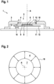
- Figure 1 shows a schematic representation of an imaging apparatus 1 as an embodiment of the invention.
- the imaging apparatus 1 can be especially part of a camera for any application.
- the imaging apparatus 1 is used in high quality applications, which need subpixel accuracy.
- the imaging apparatus 1 comprises an imaging sensor 2 for capturing images.
- the special construction of the imaging apparatus 1 allows to eliminate stresses and/or displacements on the imaging sensor 2 caused by uneven thermal expansion of different materials used to construct the imaging apparatus 1.
- the imaging apparatus 1 comprises a housing 3, whereby the imaging sensor 2 is arranged in the housing 3.
- the housing 3 is placed on a carrying structure 11, which can be realised as a hard and especially athermal body.
- the imaging apparatus 1 comprises a carrier glass 4, whereby the carrier glass 4 is fixed to the housing 3.
- the housing 3 has an opening 5 for receiving optical signals of the object to be captured.
- the carrier glass 4 closes the opening 5 in order to protect the inner parts of the imaging apparatus 1 against external influences, for example dirt or mechanical impacts.
- an optics (not shown) is placed on the housing 3 in order to realise an optical imaging from the object onto the imaging sensor 2.
- the opening 5 is smaller in the dimensions than the carrier glass 4, whereby the carrier glass 4 is arranged in the inside of the housing 3 and may contact the housing 3 in axial direction from the inside.
- the imaging sensor 2 is attached directly to the carrier glass 4. Especially the imaging sensor 2 contacts the carrier glass 4, whereby between the imaging sensor 2 and the carrier glass 4 optical adhesive 6 is arranged in order to connect the imaging sensor 2 and the carrier glass 4.
- the imaging sensor 2 is mechanically decoupled from the carrying structure 11, so that with this method, stresses originating from fixation of the imaging sensor 2 to the housing 3 are eliminated.
- the imaging sensor 2 comprises an isolation glass 7 and a sensor element 8, which is placed in optical direction under the isolation glass 7 in order to protect the sensor element 8.
- the imaging sensor 2 may further comprise a sensor casing 9, which houses the sensor element 8 and which is closed by the isolation glass 7.
- the sensor element 8 is for example a CCD- or CMOS- matrix-element.
- the sensor casing 9 may be made of ceramic or another athermal material. In order to minimise displacements, stresses and tensions resulting from temperature changes, only the isolation glass 7 is glued to the carrier glass 4 by the optical adhesive 6.
- the sensor casing 9 is not connected to the carrier glass 4, so that the contact area between imaging sensor and carrier glass 4 is realised as a glass-to-glass contact area.
- Figure 2 shows a top view only of the glass section of the imaging apparatus 1.
- the carrier glass 4 as well as the isolation glass 7 are circular shaped and are arranged coaxial to an optical and/or mechanical axis A of the glasses 4, 7.
- the optical adhesive 6 is distributed over the complete contact area of the carrier glass 4 with the isolation glass 7.
- the optical adhesive 6 is optical clear in order to prevent a reduction of optical quality by the optical signals of the image passing the contact area of the glasses 4, 7.
- the displacement of the imaging sensor 2 relative to the carrier glass 4 is minimised as all resulting stresses and tensions are symmetrically distributed around the optical and/or mechanical axis A of the glasses 4, 7. Consequently, the image position on the imaging sensor 2 and thus on the sensor element 8 is kept constant with respect to the radial direction to the optical and/or mechanical axis A of the glasses 4, 7.
- the isolation glass 7 is rectangular. In this case, the circular shaped carrier glass 4 reduces at least the displacements in radial direction.
- the carrier glass 4 is fixed to the housing 3 by our mechanical adhesive 10.
- the mechanical adhesive 10 is arranged in a circular ring ( figure 2 ) between the carrier glass 4 and the housing 3.
- the mechanical adhesive 10 is arranged at the outer lateral surface and/or outer circumference of the carrier glass 4. In axial direction, no mechanical adhesive 10 is arranged between the carrier glass 4 and the housing 3.
- the carrier glass 4 may expand in radical direction, which will be received and compensated by the mechanical adhesive 10, which is made from an elastic material.
- an expansion gap 12 is formed into the housing 3, whereby the expansion gap 12 is arranged adjacent to the circular shaped mechanical adhesive 10.
- the expansion gap 12 allows an expansion of the mechanical adhesive 10 in axial direction in case the carrier glass 4 expands in radial direction with respect to the mechanical and/or optical axis A. In the other axial direction of the mechanical adhesive 10, there's free space, so that the mechanical adhesive 10 can expand freely in both axial direction. Consequently, the image position on the imaging sensor 2 and thus on the sensor element 8 is kept constant with respect to the radial direction to the optical and/or mechanical axis A of the glasses 4, 7.
- the imaging apparatus 1 further comprises a printed circuit board 13, whereby the imaging sensor 2 is placed onto the printed circuit board 13. Especially, the imaging sensor 2 is mechanically coupled to the printed circuit board 13.
- Printed circuit boards in general are known as being anisotropic in view of temperature changes. In order to eliminate displacements, stresses and tensions resulting from the anisotropic behavior of the printed circuit board 13, the printed circuit board 13 is mechanically decoupled from the carrying structure 11 by a mechanical decoupling element 14.
- the mechanical decoupling element 14 can for example be realised as a loose cable, which is not able to transmit forces.
- Other embodiments of the decoupling element 14 are possible, for example mechanical construction which allows a relative movement between the printed circuit board 13 and the carrier structure 11 while transferring electrical signals from the printed circuit board 13 to the carrying structure 11.
- the printed circuit board 13 is mechanically connected to the imaging sensor 2 and is mechanically decoupled from the carrying structure 11 and thus from the housing 3. Consequently, displacements, stresses and tensions resulting from the movement of the printed circuit board 13 are not transferred to the housing 3 or influence the position of the imaging sensor 2 so that the sensor element 8 is kept constant with respect to the radial direction to the optical and/or mechanical axis A of the glasses 4, 7.
- Deformation and displacement of imaging sensor in precision imaging systems requiring sub-pixel stability is functionally critical. Temperature changes due to environmental variations and/or operational thermal loads cause dimensional changes on materials. These dimensional changes are related to material properties and are different for different materials. When different materials come in contact with each other, mentioned thermal induced dimension changes may create stresses on parts resulting in deformations and/or displacements. Deformations may create distorted or unsharp images and displacements cause misalignment with optimum optical axis and sharpness gradient.
- Imaging sensors are typically composed of a sensor element encased in a ceramic enclosure and covered by a transparent window typically made of glass. Sensors are soldered to printed circuit boards (PCB) to provide the necessary electrical connections which are needed to operate them. Most of the time PCB also serves as the mechanical mounting interface for imaging sensor.
- PCB printed circuit boards
- Imaging sensors are mounted on printed circuit boards both to provide necessary electrical connections and to support the sensor mechanically. Differences in material properties between PCB and sensor housing may result in displacements and stresses within operational temperature range.
- Imaging sensors normally contain a rectangular front glass to isolate sensor die from environment. If this front glass is bonded to a "carrier glass” using an optically clear adhesive, then this carrier glass can be used as the mechanical interface for sensor assembly.
- the carrier glass can be a plain window or an optical filter glass. Since both the sensor front glass and carrier glass are made from same/similar isotropic materials, misalignment due to relative displacement and stresses would not occur or be significantly reduced. In precision imaging systems, especially the ones requiring sub-pixel stability, supporting image sensor by a carrier glass having similar properties with sensor cover glass, provides better performance compared to conventional method of using sensor PCB as mechanical support.
Landscapes
- Engineering & Computer Science (AREA)
- Multimedia (AREA)
- Signal Processing (AREA)
- Physics & Mathematics (AREA)
- Electromagnetism (AREA)
- Transforming Light Signals Into Electric Signals (AREA)
Priority Applications (1)
| Application Number | Priority Date | Filing Date | Title |
|---|---|---|---|
| EP21195504.2A EP4149103B1 (fr) | 2021-09-08 | 2021-09-08 | Appareil d'imagerie à montage athermique |
Applications Claiming Priority (1)
| Application Number | Priority Date | Filing Date | Title |
|---|---|---|---|
| EP21195504.2A EP4149103B1 (fr) | 2021-09-08 | 2021-09-08 | Appareil d'imagerie à montage athermique |
Publications (2)
| Publication Number | Publication Date |
|---|---|
| EP4149103A1 true EP4149103A1 (fr) | 2023-03-15 |
| EP4149103B1 EP4149103B1 (fr) | 2025-02-26 |
Family
ID=77666360
Family Applications (1)
| Application Number | Title | Priority Date | Filing Date |
|---|---|---|---|
| EP21195504.2A Active EP4149103B1 (fr) | 2021-09-08 | 2021-09-08 | Appareil d'imagerie à montage athermique |
Country Status (1)
| Country | Link |
|---|---|
| EP (1) | EP4149103B1 (fr) |
Citations (5)
| Publication number | Priority date | Publication date | Assignee | Title |
|---|---|---|---|---|
| US20130329026A1 (en) * | 2012-03-26 | 2013-12-12 | Fujikura Ltd. | Imaging mechanism, endoscope, and method of manufacturing imaging mechanism |
| EP3061384A1 (fr) * | 2014-05-21 | 2016-08-31 | Olympus Corporation | Unité de capture d'image et endoscope |
| EP1668891B1 (fr) | 2003-08-06 | 2017-01-11 | Robert Bosch Gmbh | Systeme d'acquisition d'images |
| US20180182797A1 (en) * | 2016-11-28 | 2018-06-28 | Omnivision Technologies, Inc. | System-in-package image sensor |
| CN109120758A (zh) * | 2018-10-09 | 2019-01-01 | Oppo广东移动通信有限公司 | 光线发射器、飞行时间模组以及电子设备 |
-
2021
- 2021-09-08 EP EP21195504.2A patent/EP4149103B1/fr active Active
Patent Citations (5)
| Publication number | Priority date | Publication date | Assignee | Title |
|---|---|---|---|---|
| EP1668891B1 (fr) | 2003-08-06 | 2017-01-11 | Robert Bosch Gmbh | Systeme d'acquisition d'images |
| US20130329026A1 (en) * | 2012-03-26 | 2013-12-12 | Fujikura Ltd. | Imaging mechanism, endoscope, and method of manufacturing imaging mechanism |
| EP3061384A1 (fr) * | 2014-05-21 | 2016-08-31 | Olympus Corporation | Unité de capture d'image et endoscope |
| US20180182797A1 (en) * | 2016-11-28 | 2018-06-28 | Omnivision Technologies, Inc. | System-in-package image sensor |
| CN109120758A (zh) * | 2018-10-09 | 2019-01-01 | Oppo广东移动通信有限公司 | 光线发射器、飞行时间模组以及电子设备 |
Also Published As
| Publication number | Publication date |
|---|---|
| EP4149103B1 (fr) | 2025-02-26 |
Similar Documents
| Publication | Publication Date | Title |
|---|---|---|
| EP3244246B1 (fr) | Module de caméra pour véhicule à moteur | |
| US10750064B2 (en) | Camera for vehicle vision system with enhanced alignment features | |
| JP5795422B2 (ja) | 発熱素子を有するカメラ | |
| US8970700B2 (en) | Imaging apparatus | |
| CN110557530A (zh) | 双相机模块和便携式电子装置 | |
| JP6191541B2 (ja) | 撮像装置のレンズモジュール | |
| JP7409794B2 (ja) | レンズユニットおよびカメラモジュール | |
| US20240231033A1 (en) | Imaging lens assembly, imaging apparatus and electronic device | |
| JP4836845B2 (ja) | 水中カメラモジュール、水中カメラモジュールを備えた監視装置および水中カメラモジュールの使用方法 | |
| EP4149103B1 (fr) | Appareil d'imagerie à montage athermique | |
| JP2020016687A (ja) | レンズユニットおよびカメラモジュール | |
| EP0896202A3 (fr) | Dispositif et procédé pour examiner un élément de zone | |
| JP2010224298A (ja) | 撮像装置 | |
| US20140063753A1 (en) | Electronic module, electronic device, and mobile unit | |
| EP4148484B1 (fr) | Appareil d'imagerie avec athermalisation de la distance focale axiale | |
| JP2005295050A (ja) | カメラモジュール | |
| EP3471391B1 (fr) | Caméra | |
| US20060239632A1 (en) | Optical module and optical system | |
| US7609462B2 (en) | Optoelectronic module | |
| JP7656117B2 (ja) | 車載用撮像装置 | |
| KR101055474B1 (ko) | 카메라모듈 | |
| CN220754938U (zh) | 摄像模组和汽车 | |
| JP2025039525A (ja) | 光学機器、車載カメラ、及び、輸送機器 | |
| JP2026023658A (ja) | 撮像装置、車載カメラ、及び、輸送機器 | |
| US20250088724A1 (en) | Optical apparatus, vehicle-mounted camera, and transportation apparatus |
Legal Events
| Date | Code | Title | Description |
|---|---|---|---|
| PUAI | Public reference made under article 153(3) epc to a published international application that has entered the european phase |
Free format text: ORIGINAL CODE: 0009012 |
|
| STAA | Information on the status of an ep patent application or granted ep patent |
Free format text: STATUS: THE APPLICATION HAS BEEN PUBLISHED |
|
| AK | Designated contracting states |
Kind code of ref document: A1 Designated state(s): AL AT BE BG CH CY CZ DE DK EE ES FI FR GB GR HR HU IE IS IT LI LT LU LV MC MK MT NL NO PL PT RO RS SE SI SK SM TR |
|
| STAA | Information on the status of an ep patent application or granted ep patent |
Free format text: STATUS: REQUEST FOR EXAMINATION WAS MADE |
|
| 17P | Request for examination filed |
Effective date: 20230915 |
|
| RBV | Designated contracting states (corrected) |
Designated state(s): AL AT BE BG CH CY CZ DE DK EE ES FI FR GB GR HR HU IE IS IT LI LT LU LV MC MK MT NL NO PL PT RO RS SE SI SK SM TR |
|
| REG | Reference to a national code |
Ref country code: DE Ref legal event code: R079 Ref document number: 602021026682 Country of ref document: DE Free format text: PREVIOUS MAIN CLASS: H04N0005225000 Ipc: G02B0007000000 |
|
| GRAP | Despatch of communication of intention to grant a patent |
Free format text: ORIGINAL CODE: EPIDOSNIGR1 |
|
| STAA | Information on the status of an ep patent application or granted ep patent |
Free format text: STATUS: GRANT OF PATENT IS INTENDED |
|
| RIC1 | Information provided on ipc code assigned before grant |
Ipc: H04N 23/54 20230101ALI20240930BHEP Ipc: H04N 23/52 20230101ALI20240930BHEP Ipc: H01L 27/146 20060101ALI20240930BHEP Ipc: G02B 7/00 20210101AFI20240930BHEP |
|
| INTG | Intention to grant announced |
Effective date: 20241022 |
|
| GRAS | Grant fee paid |
Free format text: ORIGINAL CODE: EPIDOSNIGR3 |
|
| GRAA | (expected) grant |
Free format text: ORIGINAL CODE: 0009210 |
|
| STAA | Information on the status of an ep patent application or granted ep patent |
Free format text: STATUS: THE PATENT HAS BEEN GRANTED |
|
| AK | Designated contracting states |
Kind code of ref document: B1 Designated state(s): AL AT BE BG CH CY CZ DE DK EE ES FI FR GB GR HR HU IE IS IT LI LT LU LV MC MK MT NL NO PL PT RO RS SE SI SK SM TR |
|
| REG | Reference to a national code |
Ref country code: GB Ref legal event code: FG4D |
|
| REG | Reference to a national code |
Ref country code: CH Ref legal event code: EP |
|
| REG | Reference to a national code |
Ref country code: DE Ref legal event code: R096 Ref document number: 602021026682 Country of ref document: DE |
|
| REG | Reference to a national code |
Ref country code: IE Ref legal event code: FG4D |
|
| REG | Reference to a national code |
Ref country code: NL Ref legal event code: MP Effective date: 20250226 |
|
| PG25 | Lapsed in a contracting state [announced via postgrant information from national office to epo] |
Ref country code: RS Free format text: LAPSE BECAUSE OF FAILURE TO SUBMIT A TRANSLATION OF THE DESCRIPTION OR TO PAY THE FEE WITHIN THE PRESCRIBED TIME-LIMIT Effective date: 20250526 |
|
| PG25 | Lapsed in a contracting state [announced via postgrant information from national office to epo] |
Ref country code: FI Free format text: LAPSE BECAUSE OF FAILURE TO SUBMIT A TRANSLATION OF THE DESCRIPTION OR TO PAY THE FEE WITHIN THE PRESCRIBED TIME-LIMIT Effective date: 20250226 |
|
| PG25 | Lapsed in a contracting state [announced via postgrant information from national office to epo] |
Ref country code: PL Free format text: LAPSE BECAUSE OF FAILURE TO SUBMIT A TRANSLATION OF THE DESCRIPTION OR TO PAY THE FEE WITHIN THE PRESCRIBED TIME-LIMIT Effective date: 20250226 |
|
| PG25 | Lapsed in a contracting state [announced via postgrant information from national office to epo] |
Ref country code: ES Free format text: LAPSE BECAUSE OF FAILURE TO SUBMIT A TRANSLATION OF THE DESCRIPTION OR TO PAY THE FEE WITHIN THE PRESCRIBED TIME-LIMIT Effective date: 20250226 |
|
| REG | Reference to a national code |
Ref country code: LT Ref legal event code: MG9D |
|
| PG25 | Lapsed in a contracting state [announced via postgrant information from national office to epo] |
Ref country code: IS Free format text: LAPSE BECAUSE OF FAILURE TO SUBMIT A TRANSLATION OF THE DESCRIPTION OR TO PAY THE FEE WITHIN THE PRESCRIBED TIME-LIMIT Effective date: 20250626 Ref country code: NO Free format text: LAPSE BECAUSE OF FAILURE TO SUBMIT A TRANSLATION OF THE DESCRIPTION OR TO PAY THE FEE WITHIN THE PRESCRIBED TIME-LIMIT Effective date: 20250526 |
|
| PG25 | Lapsed in a contracting state [announced via postgrant information from national office to epo] |
Ref country code: NL Free format text: LAPSE BECAUSE OF FAILURE TO SUBMIT A TRANSLATION OF THE DESCRIPTION OR TO PAY THE FEE WITHIN THE PRESCRIBED TIME-LIMIT Effective date: 20250226 |
|
| PG25 | Lapsed in a contracting state [announced via postgrant information from national office to epo] |
Ref country code: HR Free format text: LAPSE BECAUSE OF FAILURE TO SUBMIT A TRANSLATION OF THE DESCRIPTION OR TO PAY THE FEE WITHIN THE PRESCRIBED TIME-LIMIT Effective date: 20250226 |
|
| PG25 | Lapsed in a contracting state [announced via postgrant information from national office to epo] |
Ref country code: PT Free format text: LAPSE BECAUSE OF FAILURE TO SUBMIT A TRANSLATION OF THE DESCRIPTION OR TO PAY THE FEE WITHIN THE PRESCRIBED TIME-LIMIT Effective date: 20250626 Ref country code: LV Free format text: LAPSE BECAUSE OF FAILURE TO SUBMIT A TRANSLATION OF THE DESCRIPTION OR TO PAY THE FEE WITHIN THE PRESCRIBED TIME-LIMIT Effective date: 20250226 |
|
| PG25 | Lapsed in a contracting state [announced via postgrant information from national office to epo] |
Ref country code: BG Free format text: LAPSE BECAUSE OF FAILURE TO SUBMIT A TRANSLATION OF THE DESCRIPTION OR TO PAY THE FEE WITHIN THE PRESCRIBED TIME-LIMIT Effective date: 20250226 Ref country code: GR Free format text: LAPSE BECAUSE OF FAILURE TO SUBMIT A TRANSLATION OF THE DESCRIPTION OR TO PAY THE FEE WITHIN THE PRESCRIBED TIME-LIMIT Effective date: 20250527 |
|
| REG | Reference to a national code |
Ref country code: AT Ref legal event code: MK05 Ref document number: 1771182 Country of ref document: AT Kind code of ref document: T Effective date: 20250226 |
|
| PG25 | Lapsed in a contracting state [announced via postgrant information from national office to epo] |
Ref country code: SE Free format text: LAPSE BECAUSE OF FAILURE TO SUBMIT A TRANSLATION OF THE DESCRIPTION OR TO PAY THE FEE WITHIN THE PRESCRIBED TIME-LIMIT Effective date: 20250226 |
|
| PG25 | Lapsed in a contracting state [announced via postgrant information from national office to epo] |
Ref country code: SM Free format text: LAPSE BECAUSE OF FAILURE TO SUBMIT A TRANSLATION OF THE DESCRIPTION OR TO PAY THE FEE WITHIN THE PRESCRIBED TIME-LIMIT Effective date: 20250226 |
|
| PG25 | Lapsed in a contracting state [announced via postgrant information from national office to epo] |
Ref country code: DK Free format text: LAPSE BECAUSE OF FAILURE TO SUBMIT A TRANSLATION OF THE DESCRIPTION OR TO PAY THE FEE WITHIN THE PRESCRIBED TIME-LIMIT Effective date: 20250226 |
|
| PG25 | Lapsed in a contracting state [announced via postgrant information from national office to epo] |
Ref country code: IT Free format text: LAPSE BECAUSE OF FAILURE TO SUBMIT A TRANSLATION OF THE DESCRIPTION OR TO PAY THE FEE WITHIN THE PRESCRIBED TIME-LIMIT Effective date: 20250226 |
|
| PGFP | Annual fee paid to national office [announced via postgrant information from national office to epo] |
Ref country code: GB Payment date: 20250923 Year of fee payment: 5 |
|
| PG25 | Lapsed in a contracting state [announced via postgrant information from national office to epo] |
Ref country code: AT Free format text: LAPSE BECAUSE OF FAILURE TO SUBMIT A TRANSLATION OF THE DESCRIPTION OR TO PAY THE FEE WITHIN THE PRESCRIBED TIME-LIMIT Effective date: 20250226 |
|
| PGFP | Annual fee paid to national office [announced via postgrant information from national office to epo] |
Ref country code: FR Payment date: 20250924 Year of fee payment: 5 |
|
| PG25 | Lapsed in a contracting state [announced via postgrant information from national office to epo] |
Ref country code: CZ Free format text: LAPSE BECAUSE OF FAILURE TO SUBMIT A TRANSLATION OF THE DESCRIPTION OR TO PAY THE FEE WITHIN THE PRESCRIBED TIME-LIMIT Effective date: 20250226 Ref country code: EE Free format text: LAPSE BECAUSE OF FAILURE TO SUBMIT A TRANSLATION OF THE DESCRIPTION OR TO PAY THE FEE WITHIN THE PRESCRIBED TIME-LIMIT Effective date: 20250226 |
|
| PG25 | Lapsed in a contracting state [announced via postgrant information from national office to epo] |
Ref country code: RO Free format text: LAPSE BECAUSE OF FAILURE TO SUBMIT A TRANSLATION OF THE DESCRIPTION OR TO PAY THE FEE WITHIN THE PRESCRIBED TIME-LIMIT Effective date: 20250226 |
|
| PG25 | Lapsed in a contracting state [announced via postgrant information from national office to epo] |
Ref country code: SK Free format text: LAPSE BECAUSE OF FAILURE TO SUBMIT A TRANSLATION OF THE DESCRIPTION OR TO PAY THE FEE WITHIN THE PRESCRIBED TIME-LIMIT Effective date: 20250226 |
|
| REG | Reference to a national code |
Ref country code: DE Ref legal event code: R097 Ref document number: 602021026682 Country of ref document: DE |
|
| PLBE | No opposition filed within time limit |
Free format text: ORIGINAL CODE: 0009261 |
|
| STAA | Information on the status of an ep patent application or granted ep patent |
Free format text: STATUS: NO OPPOSITION FILED WITHIN TIME LIMIT |
|
| REG | Reference to a national code |
Ref country code: CH Ref legal event code: L10 Free format text: ST27 STATUS EVENT CODE: U-0-0-L10-L00 (AS PROVIDED BY THE NATIONAL OFFICE) Effective date: 20260107 |
|
| PGFP | Annual fee paid to national office [announced via postgrant information from national office to epo] |
Ref country code: DE Payment date: 20251121 Year of fee payment: 5 |
|
| 26N | No opposition filed |
Effective date: 20251127 |
|
| REG | Reference to a national code |
Ref country code: CH Ref legal event code: H13 Free format text: ST27 STATUS EVENT CODE: U-0-0-H10-H13 (AS PROVIDED BY THE NATIONAL OFFICE) Effective date: 20260425 |