EP4149358B1 - Dispositif électronique et électrode comprise dans celui-ci - Google Patents
Dispositif électronique et électrode comprise dans celui-ci Download PDFInfo
- Publication number
- EP4149358B1 EP4149358B1 EP21847262.9A EP21847262A EP4149358B1 EP 4149358 B1 EP4149358 B1 EP 4149358B1 EP 21847262 A EP21847262 A EP 21847262A EP 4149358 B1 EP4149358 B1 EP 4149358B1
- Authority
- EP
- European Patent Office
- Prior art keywords
- electrode
- electronic device
- rear cover
- disposed
- conductive material
- Prior art date
- Legal status (The legal status is an assumption and is not a legal conclusion. Google has not performed a legal analysis and makes no representation as to the accuracy of the status listed.)
- Active
Links
Images


Classifications
-
- A—HUMAN NECESSITIES
- A61—MEDICAL OR VETERINARY SCIENCE; HYGIENE
- A61B—DIAGNOSIS; SURGERY; IDENTIFICATION
- A61B5/00—Measuring for diagnostic purposes; Identification of persons
- A61B5/24—Detecting, measuring or recording bioelectric or biomagnetic signals of the body or parts thereof
- A61B5/316—Modalities, i.e. specific diagnostic methods
- A61B5/318—Heart-related electrical modalities, e.g. electrocardiography [ECG]
- A61B5/332—Portable devices specially adapted therefor
-
- A—HUMAN NECESSITIES
- A61—MEDICAL OR VETERINARY SCIENCE; HYGIENE
- A61B—DIAGNOSIS; SURGERY; IDENTIFICATION
- A61B5/00—Measuring for diagnostic purposes; Identification of persons
- A61B5/24—Detecting, measuring or recording bioelectric or biomagnetic signals of the body or parts thereof
- A61B5/25—Bioelectric electrodes therefor
- A61B5/263—Bioelectric electrodes therefor characterised by the electrode materials
- A61B5/265—Bioelectric electrodes therefor characterised by the electrode materials containing silver or silver chloride
-
- A—HUMAN NECESSITIES
- A61—MEDICAL OR VETERINARY SCIENCE; HYGIENE
- A61B—DIAGNOSIS; SURGERY; IDENTIFICATION
- A61B5/00—Measuring for diagnostic purposes; Identification of persons
- A61B5/05—Detecting, measuring or recording for diagnosis by means of electric currents or magnetic fields; Measuring using microwaves or radio waves
-
- A—HUMAN NECESSITIES
- A61—MEDICAL OR VETERINARY SCIENCE; HYGIENE
- A61B—DIAGNOSIS; SURGERY; IDENTIFICATION
- A61B5/00—Measuring for diagnostic purposes; Identification of persons
- A61B5/24—Detecting, measuring or recording bioelectric or biomagnetic signals of the body or parts thereof
- A61B5/25—Bioelectric electrodes therefor
- A61B5/251—Means for maintaining electrode contact with the body
- A61B5/256—Wearable electrodes, e.g. having straps or bands
-
- A—HUMAN NECESSITIES
- A61—MEDICAL OR VETERINARY SCIENCE; HYGIENE
- A61B—DIAGNOSIS; SURGERY; IDENTIFICATION
- A61B5/00—Measuring for diagnostic purposes; Identification of persons
- A61B5/24—Detecting, measuring or recording bioelectric or biomagnetic signals of the body or parts thereof
- A61B5/25—Bioelectric electrodes therefor
- A61B5/263—Bioelectric electrodes therefor characterised by the electrode materials
-
- A—HUMAN NECESSITIES
- A61—MEDICAL OR VETERINARY SCIENCE; HYGIENE
- A61B—DIAGNOSIS; SURGERY; IDENTIFICATION
- A61B5/00—Measuring for diagnostic purposes; Identification of persons
- A61B5/24—Detecting, measuring or recording bioelectric or biomagnetic signals of the body or parts thereof
- A61B5/25—Bioelectric electrodes therefor
- A61B5/279—Bioelectric electrodes therefor specially adapted for particular uses
- A61B5/28—Bioelectric electrodes therefor specially adapted for particular uses for electrocardiography [ECG]
-
- A—HUMAN NECESSITIES
- A61—MEDICAL OR VETERINARY SCIENCE; HYGIENE
- A61B—DIAGNOSIS; SURGERY; IDENTIFICATION
- A61B5/00—Measuring for diagnostic purposes; Identification of persons
- A61B5/68—Arrangements of detecting, measuring or recording means, e.g. sensors, in relation to patient
- A61B5/6801—Arrangements of detecting, measuring or recording means, e.g. sensors, in relation to patient specially adapted to be attached to or worn on the body surface
- A61B5/6802—Sensor mounted on worn items
- A61B5/681—Wristwatch-type devices
-
- A—HUMAN NECESSITIES
- A61—MEDICAL OR VETERINARY SCIENCE; HYGIENE
- A61B—DIAGNOSIS; SURGERY; IDENTIFICATION
- A61B5/00—Measuring for diagnostic purposes; Identification of persons
- A61B5/68—Arrangements of detecting, measuring or recording means, e.g. sensors, in relation to patient
- A61B5/6887—Arrangements of detecting, measuring or recording means, e.g. sensors, in relation to patient mounted on external non-worn devices, e.g. non-medical devices
- A61B5/6898—Portable consumer electronic devices, e.g. music players, telephones, tablet computers
-
- A—HUMAN NECESSITIES
- A61—MEDICAL OR VETERINARY SCIENCE; HYGIENE
- A61B—DIAGNOSIS; SURGERY; IDENTIFICATION
- A61B5/00—Measuring for diagnostic purposes; Identification of persons
- A61B5/72—Signal processing specially adapted for physiological signals or for diagnostic purposes
- A61B5/7203—Signal processing specially adapted for physiological signals or for diagnostic purposes for noise prevention, reduction or removal
-
- H—ELECTRICITY
- H01—ELECTRIC ELEMENTS
- H01B—CABLES; CONDUCTORS; INSULATORS; SELECTION OF MATERIALS FOR THEIR CONDUCTIVE, INSULATING OR DIELECTRIC PROPERTIES
- H01B1/00—Conductors or conductive bodies characterised by the conductive materials; Selection of materials as conductors
- H01B1/02—Conductors or conductive bodies characterised by the conductive materials; Selection of materials as conductors mainly consisting of metals or alloys
-
- H—ELECTRICITY
- H01—ELECTRIC ELEMENTS
- H01B—CABLES; CONDUCTORS; INSULATORS; SELECTION OF MATERIALS FOR THEIR CONDUCTIVE, INSULATING OR DIELECTRIC PROPERTIES
- H01B1/00—Conductors or conductive bodies characterised by the conductive materials; Selection of materials as conductors
- H01B1/04—Conductors or conductive bodies characterised by the conductive materials; Selection of materials as conductors mainly consisting of carbon-silicon compounds, carbon or silicon
-
- H—ELECTRICITY
- H05—ELECTRIC TECHNIQUES NOT OTHERWISE PROVIDED FOR
- H05K—PRINTED CIRCUITS; CASINGS OR CONSTRUCTIONAL DETAILS OF ELECTRIC APPARATUS; MANUFACTURE OF ASSEMBLAGES OF ELECTRICAL COMPONENTS
- H05K5/00—Casings, cabinets or drawers for electric apparatus
- H05K5/0017—Casings, cabinets or drawers for electric apparatus with operator interface units
-
- H—ELECTRICITY
- H05—ELECTRIC TECHNIQUES NOT OTHERWISE PROVIDED FOR
- H05K—PRINTED CIRCUITS; CASINGS OR CONSTRUCTIONAL DETAILS OF ELECTRIC APPARATUS; MANUFACTURE OF ASSEMBLAGES OF ELECTRICAL COMPONENTS
- H05K5/00—Casings, cabinets or drawers for electric apparatus
- H05K5/02—Details
- H05K5/03—Covers
-
- H—ELECTRICITY
- H05—ELECTRIC TECHNIQUES NOT OTHERWISE PROVIDED FOR
- H05K—PRINTED CIRCUITS; CASINGS OR CONSTRUCTIONAL DETAILS OF ELECTRIC APPARATUS; MANUFACTURE OF ASSEMBLAGES OF ELECTRICAL COMPONENTS
- H05K7/00—Constructional details common to different types of electric apparatus
- H05K7/14—Mounting supporting structure in casing or on frame or rack
- H05K7/1422—Printed circuit boards receptacles, e.g. stacked structures, electronic circuit modules or box like frames
- H05K7/1427—Housings
-
- A—HUMAN NECESSITIES
- A61—MEDICAL OR VETERINARY SCIENCE; HYGIENE
- A61B—DIAGNOSIS; SURGERY; IDENTIFICATION
- A61B2503/00—Evaluating a particular growth phase or type of persons or animals
- A61B2503/10—Athletes
-
- A—HUMAN NECESSITIES
- A61—MEDICAL OR VETERINARY SCIENCE; HYGIENE
- A61B—DIAGNOSIS; SURGERY; IDENTIFICATION
- A61B2505/00—Evaluating, monitoring or diagnosing in the context of a particular type of medical care
- A61B2505/09—Rehabilitation or training
-
- A—HUMAN NECESSITIES
- A61—MEDICAL OR VETERINARY SCIENCE; HYGIENE
- A61B—DIAGNOSIS; SURGERY; IDENTIFICATION
- A61B2560/00—Constructional details of operational features of apparatus; Accessories for medical measuring apparatus
- A61B2560/02—Operational features
- A61B2560/0242—Operational features adapted to measure environmental factors, e.g. temperature, pollution
-
- A—HUMAN NECESSITIES
- A61—MEDICAL OR VETERINARY SCIENCE; HYGIENE
- A61B—DIAGNOSIS; SURGERY; IDENTIFICATION
- A61B2562/00—Details of sensors; Constructional details of sensor housings or probes; Accessories for sensors
- A61B2562/02—Details of sensors specially adapted for in-vivo measurements
- A61B2562/0209—Special features of electrodes classified in A61B5/24, A61B5/25, A61B5/283, A61B5/291, A61B5/296, A61B5/053
- A61B2562/0215—Silver or silver chloride containing
-
- A—HUMAN NECESSITIES
- A61—MEDICAL OR VETERINARY SCIENCE; HYGIENE
- A61B—DIAGNOSIS; SURGERY; IDENTIFICATION
- A61B2562/00—Details of sensors; Constructional details of sensor housings or probes; Accessories for sensors
- A61B2562/04—Arrangements of multiple sensors of the same type
-
- A—HUMAN NECESSITIES
- A61—MEDICAL OR VETERINARY SCIENCE; HYGIENE
- A61B—DIAGNOSIS; SURGERY; IDENTIFICATION
- A61B2562/00—Details of sensors; Constructional details of sensor housings or probes; Accessories for sensors
- A61B2562/12—Manufacturing methods specially adapted for producing sensors for in-vivo measurements
- A61B2562/125—Manufacturing methods specially adapted for producing sensors for in-vivo measurements characterised by the manufacture of electrodes
Definitions
- the disclosure relates to an electronic device and an electrode included in the same.
- wearable electronic devices are equipped with various sensors capable of measuring user's biometric information.
- the user's biometric information may be measured by recognizing an electrical signal flowing through a user body or applying an electrical signal to a user body.
- the electronic device may include an electrode to contact a user body.
- WO 2019/177769 A1 describes user interfaces for initial setup of health monitoring using a first electronic device and a second electronic device. Exemplary user interfaces for recording biometric information for use in health monitoring is described. Exemplary user interfaces for using an input device while recording biometric information for health monitoring is described. Exemplary user interfaces for viewing and managing aspects of health monitoring is described. A method performed at a first electronic device with a display and one or more input devices, wherein the first electronic device is paired with a second electronic device, is described.
- the method comprises: displaying, on the display, a first portion of a tutorial for using a function of the second electronic device; detecting, via the one or more input devices, a request to proceed with the tutorial; in response to detecting the request to proceed with the tutorial, displaying, on the display, instructions to perform an operation on the second electronic device that involves the function of the second electronic device; receiving, from the second electronic device, an indication that the instructions have been carried out; and in response to receiving the indication that the instructions have been carried out, displaying, on the display, a second portion of the tutorial that is different from the first portion.
- US 2019/101870 A1 discloses an electronic device, such as a watch, which has a housing to which a carrier is attached.
- the carrier has a first surface interior to the electronic device, and a second surface exterior to the electronic device.
- a set of electrodes is deposited on the exterior surface of the carrier.
- An additional electrode is operable to be contacted by a finger of a user of the electronic device while the first electrode is positioned against skin of the user.
- the additional electrode may be positioned on a user-rotatable crown of the electronic device, on a button of the electronic device, or on another surface of the housing of the electronic device.
- a processor of the electronic device is operable to determine a biological parameter of the user based on voltages at the electrodes.
- the biological parameter may be an electrocardiogram.
- the electrode included in the electronic device may be directly exposed to an external environment. Therefore, the electrode should be able to withstand changes in the external environment (e.g., changes in temperature, changes in humidity, or changes in light).
- changes in the external environment e.g., changes in temperature, changes in humidity, or changes in light.
- filters such as a high pass filter (HPF) and a low pass filter (LPF) are used, but there may be limitations in removing such noise.
- HPF high pass filter
- LPF low pass filter
- the electrode included in the electronic device is highly likely to be damaged when exposed to the external environment. If the electrode is damaged, the measurement quality of the bio-signal may be degraded.
- aspects of the disclosure are to address at least the above-mentioned problems and/or disadvantages and to provide at least the advantages described below. Accordingly, as aspect of the disclosure is to provide an electrode satisfying required surface resistance and durability, and an electronic device including the electrode.
- an electronic device in accordance with an aspect of the disclosure, includes a housing, a display viewable through at least a portion of a front surface of the housing, a rear cover disposed on a rear surface of the housing, a first electrode disposed on a lateral surface of the housing, and second and third electrodes disposed at different positions on the rear cover.
- the first electrode, the second electrode, and the third electrode may include a conductive material that is a compound containing titanium (Ti), aluminum (Al), chromium (Cr), silicon (Si), carbon (C), and nitrogen (N).
- an electrode of an electronic device includes a first electrode disposed on a portion of a housing of the electronic device, and second and third electrodes disposed at different positions on a rear cover disposed on a rear surface of the housing.
- the first electrode, the second electrode, and the third electrode may include a conductive material that is a compound containing titanium (Ti), aluminum (Al), chromium (Cr), silicon (Si), carbon (C), and nitrogen (N).
- the electrode having excellent durability and low surface resistance resulting in high electrical conductivity can be provided.
- This electrode not only can maintain its characteristics for a long time even when exposed to the outside of the electronic device because of having excellent durability, but also can accurately measure a bio-signal because of a low resistance.
- each of such phrases as “A or B,” “at least one of A and B,” “at least one of A or B,” “A, B, or C,” “at least one of A, B, and C,” and “at least one of A, B, or C,” may include any one of, or all possible combinations of the items enumerated together in a corresponding one of the phrases.
- such terms as “1st” and “2nd,” or “first” and “second” may be used to simply distinguish a corresponding component from another, and does not limit the components in other aspect (e.g., importance or order).
- an element e.g., a first element
- the element may be coupled with the other element directly (e.g., wiredly), wirelessly, or via a third element.
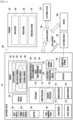
- FIG. 1 is a block diagram illustrating an electronic device 101 in a network environment 100 according to an embodiment of the disclosure.
- the electronic device 101 in the network environment 100 may communicate with an electronic device 102 via a first network 198 (e.g., a short-range wireless communication network), or at least one of an electronic device 104 or a server 108 via a second network 199 (e.g., a long-range wireless communication network).
- a first network 198 e.g., a short-range wireless communication network
- a second network 199 e.g., a long-range wireless communication network
- the electronic device 101 may communicate with the electronic device 104 via the server 108.
- the electronic device 101 may include a processor 120, memory 130, an input module 150, a sound output module 155, a display module 160, an audio module 170, a sensor module 176, an interface 177, a connecting terminal 178, a haptic module 179, a camera module 180, a power management module 188, a battery 189, a communication module 190, a subscriber identification module(SIM) 196, or an antenna module 197.
- at least one of the components e.g., the connecting terminal 178) may be omitted from the electronic device 101, or one or more other components may be added in the electronic device 101.
- some of the components e.g., the sensor module 176, the camera module 180, or the antenna module 197) may be implemented as a single component (e.g., the display module 160).
- the processor 120 may execute, for example, software (e.g., a program 140) to control at least one other component (e.g., a hardware or software component) of the electronic device 101 coupled with the processor 120, and may perform various data processing or computation. According to one embodiment, as at least part of the data processing or computation, the processor 120 may store a command or data received from another component (e.g., the sensor module 176 or the communication module 190) in volatile memory 132, process the command or the data stored in the volatile memory 132, and store resulting data in non-volatile memory 134.
- software e.g., a program 140
- the processor 120 may store a command or data received from another component (e.g., the sensor module 176 or the communication module 190) in volatile memory 132, process the command or the data stored in the volatile memory 132, and store resulting data in non-volatile memory 134.
- the processor 120 may include a main processor 121 (e.g., a central processing unit (CPU) or an application processor (AP)), or an auxiliary processor 123 (e.g., a graphics processing unit (GPU), a neural processing unit (NPU), an image signal processor (ISP), a sensor hub processor, or a communication processor (CP)) that is operable independently from, or in conjunction with, the main processor 121.
- a main processor 121 e.g., a central processing unit (CPU) or an application processor (AP)
- auxiliary processor 123 e.g., a graphics processing unit (GPU), a neural processing unit (NPU), an image signal processor (ISP), a sensor hub processor, or a communication processor (CP)
- the main processor 121 may be adapted to consume less power than the main processor 121, or to be specific to a specified function.
- the auxiliary processor 123 may be implemented as separate from, or as part of the main processor 121.
- the auxiliary processor 123 may control at least some of functions or states related to at least one component (e.g., the display module 160, the sensor module 176, or the communication module 190) among the components of the electronic device 101, instead of the main processor 121 while the main processor 121 is in an inactive (e.g., sleep) state, or together with the main processor 121 while the main processor 121 is in an active state (e.g., executing an application).
- the auxiliary processor 123 e.g., an image signal processor or a communication processor
- the auxiliary processor 123 may include a hardware structure specified for artificial intelligence model processing.
- An artificial intelligence model may be generated by machine learning. Such learning may be performed, e.g., by the electronic device 101 where the artificial intelligence is performed or via a separate server (e.g., the server 108). Learning algorithms may include, but are not limited to, e.g., supervised learning, unsupervised learning, semi-supervised learning, or reinforcement learning.
- the artificial intelligence model may include a plurality of artificial neural network layers.
- the artificial neural network may be a deep neural network (DNN), a convolutional neural network (CNN), a recurrent neural network (RNN), a restricted boltzmann machine (RBM), a deep belief network (DBN), a bidirectional recurrent deep neural network (BRDNN), deep Q-network or a combination of two or more thereof but is not limited thereto.
- the artificial intelligence model may, additionally or alternatively, include a software structure other than the hardware structure.
- the memory 130 may store various data used by at least one component (e.g., the processor 120 or the sensor module 176) of the electronic device 101.
- the various data may include, for example, software (e.g., the program 140) and input data or output data for a command related thereto.
- the memory 130 may include the volatile memory 132 or the non-volatile memory 134.
- the non-volatile memory 134 may include internal memory 136 and external memory 138.
- the program 140 may be stored in the memory 130 as software, and may include, for example, an operating system (OS) 142, middleware 144, or an application 146.
- OS operating system
- middleware middleware
- application application
- the sound output module 155 may output sound signals to the outside of the electronic device 101.
- the sound output module 155 may include, for example, a speaker or a receiver.
- the speaker may be used for general purposes, such as playing multimedia or playing record.
- the receiver may be used for receiving incoming calls. According to an embodiment, the receiver may be implemented as separate from, or as part of the speaker.
- the audio module 170 may convert a sound into an electrical signal and vice versa. According to an embodiment, the audio module 170 may obtain the sound via the input module 150, or output the sound via the sound output module 155 or a headphone of an external electronic device (e.g., an electronic device 102) directly (e.g., wiredly) or wirelessly coupled with the electronic device 101.
- an external electronic device e.g., an electronic device 102
- directly e.g., wiredly
- wirelessly e.g., wirelessly
- the interface 177 may support one or more specified protocols to be used for the electronic device 101 to be coupled with the external electronic device (e.g., the electronic device 102) directly (e.g., wiredly) or wirelessly.
- the interface 177 may include, for example, a high definition multimedia interface (HDMI), a universal serial bus (USB) interface, a secure digital (SD) card interface, or an audio interface.
- HDMI high definition multimedia interface
- USB universal serial bus
- SD secure digital
- the haptic module 179 may convert an electrical signal into a mechanical stimulus (e.g., a vibration or a movement) or electrical stimulus which may be recognized by a user via his tactile sensation or kinesthetic sensation.
- the haptic module 179 may include, for example, a motor, a piezoelectric element, or an electric stimulator.
- the camera module 180 may capture a still image or moving images.
- the camera module 180 may include one or more lenses, image sensors, image signal processors, or flashes.
- the power management module 188 may manage power supplied to the electronic device 101.
- the power management module 188 may be implemented as at least part of, for example, a power management integrated circuit (PMIC).
- PMIC power management integrated circuit
- the battery 189 may supply power to at least one component of the electronic device 101.
- the battery 189 may include, for example, a primary cell which is not rechargeable, a secondary cell which is rechargeable, or a fuel cell.
- a corresponding one of these communication modules may communicate with the external electronic device via the first network 198 (e.g., a short-range communication network, such as BluetoothTM, wireless-fidelity (Wi-Fi) direct, or infrared data association (IrDA)) or the second network 199 (e.g., a long-range communication network, such as a legacy cellular network, a 5G network, a next-generation communication network, the Internet, or a computer network (e.g., LAN or wide area network (WAN)).
- first network 198 e.g., a short-range communication network, such as BluetoothTM, wireless-fidelity (Wi-Fi) direct, or infrared data association (IrDA)
- the second network 199 e.g., a long-range communication network, such as a legacy cellular network, a 5G network, a next-generation communication network, the Internet, or a computer network (e.g., LAN or wide area network (WAN)).
- the wireless communication module 192 may support various technologies for securing performance on a high-frequency band, such as, e.g., beamforming, massive multiple-input and multiple-output (massive MIMO), full dimensional MIMO (FD-MIMO), array antenna, analog beam-forming, or large scale antenna.
- the wireless communication module 192 may support various requirements specified in the electronic device 101, an external electronic device (e.g., the electronic device 104), or a network system (e.g., the second network 199).
- the wireless communication module 192 may support a peak data rate (e.g., 20Gbps or more) for implementing eMBB, loss coverage (e.g., 164dB or less) for implementing mMTC, or U-plane latency (e.g., 0.5ms or less for each of downlink (DL) and uplink (UL), or a round trip of 1ms or less) for implementing URLLC.
- a peak data rate e.g., 20Gbps or more
- loss coverage e.g., 164dB or less
- U-plane latency e.g., 0.5ms or less for each of downlink (DL) and uplink (UL), or a round trip of 1ms or less
- the antenna module 197 may transmit or receive a signal or power to or from the outside (e.g., the external electronic device) of the electronic device 101.
- the antenna module 197 may include an antenna including a radiating element composed of a conductive material or a conductive pattern formed in or on a substrate (e.g., a printed circuit board (PCB)).
- the antenna module 197 may include a plurality of antennas (e.g., array antennas). In such a case, at least one antenna appropriate for a communication scheme used in the communication network, such as the first network 198 or the second network 199, may be selected, for example, by the communication module 190 (e.g., the wireless communication module 192) from the plurality of antennas.
- the antenna module 197 may form a mmWave antenna module.
- the mmWave antenna module may include a printed circuit board, a RFIC disposed on a first surface (e.g., the bottom surface) of the printed circuit board, or adjacent to the first surface and capable of supporting a designated high-frequency band (e.g., the mmWave band), and a plurality of antennas (e.g., array antennas) disposed on a second surface (e.g., the top or a side surface) of the printed circuit board, or adj acent to the second surface and capable of transmitting or receiving signals of the designated high-frequency band.
- a RFIC disposed on a first surface (e.g., the bottom surface) of the printed circuit board, or adjacent to the first surface and capable of supporting a designated high-frequency band (e.g., the mmWave band)
- a plurality of antennas e.g., array antennas
- At least some of the above-described components may be coupled mutually and communicate signals (e.g., commands or data) therebetween via an inter-peripheral communication scheme (e.g., a bus, general purpose input and output (GPIO), serial peripheral interface (SPI), or mobile industry processor interface (MIPI)).
- an inter-peripheral communication scheme e.g., a bus, general purpose input and output (GPIO), serial peripheral interface (SPI), or mobile industry processor interface (MIPI)
- commands or data may be transmitted or received between the electronic device 101 and the external electronic device 104 via the server 108 coupled with the second network 199.
- Each of the electronic devices 102 or 104 may be a device of a same type as, or a different type, from the electronic device 101.
- all or some of operations to be executed at the electronic device 101 may be executed at one or more of the external electronic devices 102, 104, or 108. For example, if the electronic device 101 should perform a function or a service automatically, or in response to a request from a user or another device, the electronic device 101, instead of, or in addition to, executing the function or the service, may request the one or more external electronic devices to perform at least part of the function or the service.
- the one or more external electronic devices receiving the request may perform the at least part of the function or the service requested, or an additional function or an additional service related to the request, and transfer an outcome of the performing to the electronic device 101.
- the electronic device 101 may provide the outcome, with or without further processing of the outcome, as at least part of a reply to the request.
- a cloud computing, distributed computing, mobile edge computing (MEC), or client-server computing technology may be used, for example.
- the electronic device 101 may provide ultra low-latency services using, e.g., distributed computing or mobile edge computing.
- the external electronic device 104 may include an internet-of-things (IoT) device.
- the server 108 may be an intelligent server using machine learning and/or a neural network.
- the external electronic device 104 or the server 108 may be included in the second network 199.
- the electronic device 101 may be applied to intelligent services (e.g., smart home, smart city, smart car, or healthcare) based on 5G communication technology or IoT-related technology.
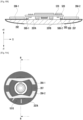
- FIG. 2 is a front perspective view illustrating a mobile electronic device according to an embodiment of the disclosure.
- FIG. 3 is a rear perspective view illustrating the electronic device of FIG. 2 according to an embodiment of the disclosure.
- FIG. 4 is an exploded perspective view illustrating the electronic device of FIG. 2 according to an embodiment of the disclosure.
- an electronic device 200 may include a housing 210 having a first surface (or front surface) 210A, a second surface (or rear surface) 210B, and a lateral surface 210C enclosing a space between the first surface 210A and the second surface 210B.
- the electronic device 200 may include fastening members 250 and 260 connected to at least a portion of the housing 210 and configured to detachably attach the electronic device 200 to a user's body part (e.g., wrist, ankle, etc.) of a user's body.
- the housing may refer to a structure forming some of the first surface 210A, the second surface 210B, and the lateral surface 210C.
- the first surface 210A may be formed at least in part by a substantially transparent front plate 201 (e.g., a polymer plate or a glass plate including various coating layers).
- the second surface 210B may be formed by a substantially opaque rear cover 207.
- the rear cover 207 may be formed by coated or colored glass, ceramic, polymer, metal (e.g., aluminum, stainless steel (STS), or magnesium), or a combination of at least two of the above materials.
- the lateral surface 210C may be formed of a lateral bezel structure 206 (or "lateral member") combined with the front plate 201 and the rear cover 207 and having a metal and/or a polymer.
- the rear cover 207 and the lateral bezel structure 206 may be integrally formed with each other and have the same material (e.g., a metal material such as aluminum), although other arrangements are possible.
- the fastening members 250 and 260 may be formed of various materials and shapes.
- the fastening members 250 and 260 may be formed integrally by woven fabric, leather, rubber, urethane, metal, ceramic, or any combination thereof, or be formed with a plurality of unit links that are flexible with each other.
- the electronic device 200 may include at least one of a display 220 (see FIG. 4 ), audio modules 205 and 208, a sensor module 211, key input devices 202 and 290, and a connector hole 209. At least one (e.g., the key input devices 202 and 290, the connector hole 209, or the sensor module 211) of the above components may be omitted.
- the electronic device 200 may further include other components not shown.
- the display 220 may be exposed through a portion of the front plate 201.
- the display 220 may have a shape corresponding to the shape of the front plate 201, and may have various shapes such as a circle, an oval, or a polygon.
- the display 220 may be disposed adjacent to or combined with a touch sensing circuit, a pressure sensor capable of measuring the intensity (or pressure) of a touch, and/or a fingerprint sensor.
- the audio modules 205 and 208 may include a microphone hole 205 and a speaker hole 208.
- the microphone hole 205 may contain a microphone for obtaining an external sound, and may contain a plurality of microphones to detect a direction of a sound.
- the speaker hole 208 may be used for an external speaker and a call receiver.
- the speaker hole 208 and the microphone hole 205 may be implemented as one hole, or a speaker (e.g., a piezo speaker) may be included without the speaker hole 208.
- the sensor module 211 may generate an electrical signal or data value corresponding to an internal operating state or external environmental state of the electronic device 200.
- the sensor module 211 may include a biometric sensor module 211 (e.g., a heart rate monitor (HRM) sensor) disposed on the second surface 210B of the housing 210.
- the electronic device 200 may further include any other sensor module (not shown) such as a gesture sensor, a gyro sensor, an air pressure sensor, a magnetic sensor, an acceleration sensor, a grip sensor, a color sensor, an infrared (IR) sensor, a biometric sensor, a temperature sensor, a humidity sensor, and/or an illumination sensor.
- HRM heart rate monitor
- the key input devices 202 and 290 may include a wheel key 202 disposed on the first surface 210A of the housing 210 and rotatable in at least one direction, and/or a side key button 290 disposed on the lateral surface 210C of the housing 210.
- the wheel key may have a shape corresponding to the shape of the front plate 201.
- One or both of the aforementioned key input devices 202 and 290 may be omitted; the key input device(s) that is/are omitted may be implemented in another form, such as a soft key on the display 220.
- the connector hole 209 is capable of accommodating a connector (e.g., a USB connector) for transmitting and receiving power and/or data to and from an external electronic device, and may include another connector hole (not shown) capable of accommodating a connector for transmitting and receiving an audio signal to and from an external electronic device.
- the electronic device 200 may further include a connector cover (not shown) that covers at least a portion of the connector hole 209 to block the inflow of external foreign substances into the connector hole.
- the fastening members 250 and 260 may be attached to and detached from at least a portion of the housing 210 through locking members 251 and 261.
- the fastening members 250 and 260 may have a band or strap shape, and may include one or more of a fixing member 252, fixing member insertion holes 253, a band guide member 254, and a band support ring 255.
- the fixing member 252 may be inserted into one of the fixing member insertion holes 253 to fix the housing 210 and the fastening members 250 and 260 to a part (e.g., wrists, ankles, etc.) of the user's body.
- the band guide member 254 may limit the range of motion of the fixing member 252 inserted into the fixing member insertion hole 253 so that the fastening members 250 and 260 may be in close contact with a part of the user's body.
- the band support ring 255 may limit the range of motion of the fastening members 250 and 260 in a state where the fixing member 252 is inserted into the fixing member insertion hole 253.
- the support member 460 may be formed of, for example, a metal material and/or a non-metal (e.g., polymer) material.
- the support member 460 may be combined with the display 220 at one side thereof and also combined with the first PCB 480 at the other side thereof.
- a processor, a memory, and/or an interface may be mounted on the first PCB 480.
- the processor may include one or more of a CPU, an application processor (AP), a graphic processing unit (GPU), a sensor processor, or a communication processor (CP).
- the battery 470 is a device for supplying power to at least one component of the electronic device 400, and may include a non-rechargeable primary battery, a rechargeable secondary battery, or a fuel cell. At least a part of the battery 470 may be disposed on substantially the same plane as the first PCB 480. The battery 470 may be disposed integrally within, or detachably from, the electronic device 400.
- the first antenna 450 may be disposed between the display 220 and the support member 460.
- the first antenna 450 may include a near field communication (NFC) antenna, a wireless charging antenna, and/or a magnetic secure transmission (MST) antenna.
- NFC near field communication
- MST magnetic secure transmission
- the first antenna 450 may perform short-range communication with an external device, wirelessly transmit and receive power required for charging, or transmit a short-range communication signal or a magnetic-based signal including payment data.
- An antenna structure may also be formed by a part or combination of the lateral bezel structure 410 and/or the support member 460.
- the sealing member 490 may be positioned between the lateral bezel structure 410 and the rear plate 493.
- the sealing member 490 may be configured to block moisture and foreign matter flowing into a space surrounded by the lateral bezel structure 410 and the rear plate 493 from the outside.
- a second PCB 520 (e.g., a PCB, a flexible PCB (FPCB), or rigid-flexible PCB (RFPCB)) and a coil 530 for wireless charging may be disposed between the rear plate 493 and the rear cover 207.
- the second PCB 520 may be electrically connected to the first PCB 480 through a hole formed in the rear plate 493.
- the wireless charging coil 530 may be disposed to surround the outer periphery of the second PCB 520.
- the electronic device may include the housing 210, the display 220 viewed through at least a portion of the first surface 210A (or front surface) of the housing 210, and the rear cover 207 disposed on the second surface 210B (or rear surface) of the housing 210.
- the electronic device may include a plurality of electrodes exposed to the outside so as to be in contact with a user's body.
- the electrode may include a first electrode 281, a second electrode 282, and a third electrode 283.
- the number of electrodes included in the electronic device may be variously changed. Hereinafter, a total of three electrodes of the electronic device will be described, but the number of electrodes included in the electronic device may be one, two, four, or more.
- At least one of the electrodes 281, 282, and 283 of the electronic device 200 may be disposed at least one of a position of the key input device 202 or 290, a position of the lateral bezel structure 206, a position of the display 220, or a position of the housing 210.
- the first electrode 281 may be disposed on the lateral surface 210C of the electronic device housing 210. As shown in FIG. 2 , the first electrode 281 may be formed on at least one of the buttons 290 disposed on the lateral surface 210C of the housing 210.
- the button 290 disposed on the lateral surface 210C of the housing 210 may be a physical button that is pressed by the user's body and moves forward and backward with respect to the housing 210, or a touch button that recognizes contact with the user's body.
- the button 290 may be formed of a conductive substance, and the first electrode 281 may be formed on the button 290.
- the second electrode 282 and the third electrode 283 may be disposed on the rear cover 207 forming the rear surface 210B of the electronic device housing 210.
- the second electrode 282 and the third electrode 283 may be disposed at different positions on the rear cover 207.
- the second electrode 282 and the third electrode 283 may be electrically isolated from each other on the rear cover 207.
- At least one of the first electrode 281, the second electrode 282, and the third electrode 283 may be an electrode that contacts the user's skin and is capable of measuring an electrical signal according to the user's physical activity.
- at least one of the first electrode 281, the second electrode 282, and the third electrode 283 may contact the user's skin and measure an electrical signal according to the user's heartbeat.
- an electrode e.g., the first electrode 281, the second electrode 282, or the third electrode 283 in FIGS. 2 and 3
- An electronic device e.g., the electronic device 400 in FIG. 4
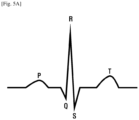
- the body information measured through the electrode may be information related to a heartbeat.
- the electrode may measure a user's electrocardiogram (ECG) signal.
- ECG electrocardiogram
- the heartbeat may be identified through an electrical signal.
- the potential difference may be affected by a difference in a material forming the electrode that is in contact with the user's body.
- the material forming the electrode has a unique oxidation reduction potential (or equilibrium oxidation reduction potential) for each material.
- the oxidation-reduction potential refers to a potential value for maintaining an equilibrium state in which an oxidation-reduction reaction does not occur because of the same oxidation and reduction rates.
- the electrodes disposed at different parts of the user's body for ECG measurement have different materials, a difference in the oxidation-reduction potential may be reflected in the ECG signal as it is.
- the potential difference due to the difference in the materials forming the electrodes may be mainly reflected in a low potential difference portion (e.g., 0 ⁇ 0.2 mV portion in FIG. 5B ) in the ECG signal.
- the potential difference when the potential difference is calculated through the electrodes disposed at different parts of the user's body, the user's body acts as a resistance, and the resistance value may be reflected in the ECG signal. Therefore, in order to reduce the resistance caused by the user's body, a signal transmission path of the electrode may be formed to be short.
- the electrode should be able to measure sensitive changes in the bioelectric signal, which may be related to the electrical conductivity of the electrode.
- a plurality of electrodes contacting the user's body may be formed of the same material having high electric conductivity.
- the rear cover 207 disposed on the rear surface 210B of the housing 210 may be in contact with the user's wrist in a state where the electronic device is worn.
- the second electrode 282 and the third electrode 283 may be disposed on the rear cover 207, so that the second and third electrodes 282 and 283 may be in contact with the user's wrist while the user is wearing the electronic device.
- a finger of a hand without the electronic device may be brought into contact with the first electrode 281 disposed on the lateral surface 210C of the electronic device housing 210.
- the first electrode 281 may be in contact with the finger of one hand of the user, and the second and third electrodes 282 and 283 may be in contact with the wrist of the other hand of the user. It is therefore possible to measure the ECG signal through a potential difference between the electrodes disposed at different parts of the body.
- the first electrode 281, the second electrode 282, and the third electrode 283 may include the same conductive material.
- the conductive material included in the electrode may have high electrical conductivity so as to detect fine current changes in skin well.
- the electrode included in the electronic device should not change its characteristics even by external factors such as temperature, humidity, and light, and should be resistant to impact or corrosion because of being exposed to the outside of the electronic device.
- the electrode that is in contact with the user's body may be formed of a hypoallergenic material with little skin irritation.
- the conductive material used for the electrode of the electronic device may have high electrical conductivity and high durability.
- the electrode included in the electronic device may be an electrode having a Mohs hardness (MOHS) of 5 or more.
- FIG. 6A is a diagram illustrating a composition of a conductive material included in an electrode according to an embodiment of the disclosure.
- the first electrode 281, the second electrode 282, and the third electrode 283 may include at least one material having high durability and high electric conductivity.
- the first electrode 281, the second electrode 282, and the third electrode 283 may include at least one of an oxide-based material, a nitride-based material, and/or a carbide-based material.
- oxide-based materials may include transparent materials such as indium tin oxide (ITO), tin oxide (SnO), zinc oxide (ZnO), and fluorine-doped tin oxide (FTO), and/or opaque materials such as titanium dioxide (TiO 2 ).
- Nitride-based materials may include chromium nitride (CrN), chromium carbon-nitride (CrCN), chromium silicon carbon nitride (CrSiCN), titanium nitride (TiN), titanium carbon nitride (TiCN), chromium boron carbon nitride (CrBCN), chromium boron silicon carbon nitride (CrBSiCN), chromium titanium carbon nitride (CrTiCN), chromium titanium silicon carbon nitride (CrTiSiCN), chromium aluminum carbon nitride (CrAlCN), and chromium aluminum silicon carbon nitride (CrAlSiCN).
- Carbide-based materials may include tungsten carbide (WC) and titanium carbide (TiC).
- the first electrode 281, the second electrode 282, and the third electrode 283 may use TiAlCrSiCN (hereinafter referred to as "conductive material"), which is a compound containing titanium (Ti), aluminum (Al), chromium (Cr), silicon (Si), carbon (C) and nitrogen (N) as conductive materials.
- the conductive material may have high durability as well as high electric conductivity.
- a CrSiCN material containing chromium, silicon, carbon and nitrogen has high electrical conductivity and high durability, so it may be advantageous for surface coating. Adding titanium to the CrSiCN material can improve electrical properties (e.g., electric conductivity), and adding aluminum can improve heat resistance and thereby improve durability.
- compositions of the electrodes may be different.
- composition may be adjusted depending on the positions where the electrodes are disposed. For example, an electrode disposed at a position that is in continuous contact with the user's body may be adjusted in composition to increase durability, and an electrode disposed at a position that is in intermittent contact with the user's body may be adjusted in composition to increase electrical conductivity.
- an electrode disposed at a position that is in continuous contact with the user's body may be adjusted in composition to increase durability
- an electrode disposed at a position that is in intermittent contact with the user's body may be adjusted in composition to increase electrical conductivity.
- the content of titanium increases, the electrical conductivity of the conductive material may increase, but the strength and hardness of the conductive material may decrease, and the frictional force of the surface may increase.
- the composition of titanium may be about 1 to 7% by weight. If the content of aluminum increases, the color becomes dark and the heat resistance may be enhanced. However, if the aluminum composition exceeds a certain threshold, the conductive material may have a red color.
- the composition of aluminum may be about 1 to 7% by weight. Chromium may improve the corrosion resistance of the conductive material, but may increase the reflectivity of the conductive material. The composition of chromium may be about 15 to 35% by weight. Silicon may improve the hardness of the conductive material by smoothing the surface, but if the composition of silicon exceeds a certain threshold, the strength of the conductive material may decrease. The composition of silicon may be about 3 to 15% by weight. Carbon may darken the color of the conductive material. The composition of carbon may be about 8 to 25% by weight. The conductive material containing a certain ratio of nitrogen may have improved hardness. The composition of nitrogen may be about 15 to 35% by weight.
- the composition of the conductive material may be adjusted by regulating several parameters in deposition equipment.
- Sputter or e-beam may be used as the deposition equipment,.
- a target since the number of targets in a deposition equipment chamber is limited, a target may be formed by using several materials alone or in combination, and a composition ratio may be adjusted by regulating several parameters in each chamber.
- Titanium (Ti), aluminum (Al), chromium (Cr), and silicon (Si) may be used alone or in combination to form a target.
- the target composition ratio that is, the ratio of titanium to aluminum may be a ratio of about 30-50% to about 50-70%.
- Chromium and silicon may be used alone or in combination to form a target.
- the ratio of chromium to silicon may be a ratio of about 40-60% to about 40-60%.
- Carbon may be used alone to form a target. Gaseous carbon may also be used. In this case, carbon can be obtained from acetylene (C 2 H 2 ). In case of nitrogen, gaseous nitrogen may be used.
- the composition of the conductive material may be adjusted through the power of the target.
- the power of the target may be, for example, about 2 to 5 kW in case of titanium or aluminum, about 1 to 6 kW in case of chromium, and about 2 to 8 kW in case of silicon.
- a power of about 4 to 8 kW may be used.
- a power of about 3 to 6 kW may be used.
- the gas flow may be about 10 to 60 sccm, and when a gaseous nitrogen is used, the gas flow may be 30 to 400 sccm.
- Table 1 shows a comparison of the surface resistance, resistance fluctuation, and surface hardness between TiAlCrSiCN containing titanium (Ti), aluminum (Al), chromium (Cr), silicon (Si), carbon (C) and nitrogen (N) and CrSiCN containing chromium (Cr), silicon (Si), carbon (C) and nitrogen (N).
- the first material is a compound composed of chromium of about 35%, silicon of about 15%, carbon of about 10%, and nitrogen of about 40%.
- the second material is a compound composed of titanium of about 3%, aluminum of about 5%, chromium of about 35%, silicon of about 11%, carbon of about 12%, and nitrogen of about 34%.
- the third material is a compound composed of titanium of about 6%, aluminum of about 4%, chromium of about 34%, silicon of about 15%, carbon of about 9%, and nitrogen of about 32%.
- the second material and the third material may be understood as the conductive materials disclosed herein.
- the second and third materials may be advantageous in measuring a bio-signal.
- the surface hardness of the second and third materials is Mohs hardness of 5, which is the same as that of the first material.
- FIG. 6B is a graph illustrating electrical properties of a conductive material according to an embodiment of the disclosure.
- a graph (a) shows the electrical properties of a compound according to the related art, which is composed of chromium (Cr), silicon (Si), carbon (C), and nitrogen (N) (hereinafter referred to as "material according to the related art").
- a graph (b) shows the electrical properties of a conductive material composed of titanium (Ti), aluminum (Al), chromium (Cr), silicon (Si), carbon (C), and nitrogen (N) described above. Such graphs show the resistance, reactance, and phase of each material according to frequency.
- the resistance of the conductive material is lower than that of the material according to the related art in all frequency ranges. Since it is possible to receive a higher quality signal through a material having a lower resistance, the conductive material may be more advantageous in receiving a higher quality signal than the material according to the related art. In addition, it can be seen that the resistance of the material appears differently depending on the frequency, whereas the resistance of the conductive material is maintained at a constant level even with a frequency change. Therefore, the conductive material can perform a more stable measurement.
- the conductive material In case of the conductive material, it can be seen that a phase change of current and voltage at different frequencies is not large, and thus a change in reactance is not large. On the other hand, in case of the material, it can be seen that the phase change of current and voltage appears large at different frequencies, and the change in reactance is also relatively large according to the related art.
- the conductive material having a small phase change of current and voltage even in different frequency ranges can measure electrical signals more stably than the material having a large phase change according to the related art.
- FIGS. 7A-7B are perspective views illustrating a button of an electronic device according to various embodiment of the disclosure.
- At least a portion of an outer surface 710 of the button 290 may include a non-conductive material.
- a portion of the outer surface 710 of the button 290 may be formed of an organic material, a ceramic material, or a combination thereof.
- a portion of the lateral surface 210C where the button 290 is positioned includes a conductive substance
- at least a portion of the outer surface 710 of the button 290 being in contact with the conductive substance of the lateral surface 210C may include a non-conductive material.
- an upper surface 720 and a lower surface 730 of the button 290 may not include a non-conductive material.
- the upper surface 720 of the button 290 may be a part to be in contact with the user's body (e.g., user's finger), and the lower surface 730 of the button 290 may be a part being in contact with a terminal installed on a PCB (e.g., the FPCB 520 in FIG. 4 ).
- a PCB e.g., the FPCB 520 in FIG. 4
- At least one of the upper and lower surfaces 720 and 730 of the button 290 may include the above-described conductive material (TiAlCrSiCN).
- TiAlCrSiCN conductive material
- both the upper surface 720 and the lower surface 730 of the button 290 may include the conductive material.
- the upper surface 720 of the button 290 including the first electrode 281 may be exposed to the outside of the electronic device. If the upper surface 720 exposed to the outside includes a conductive material, it is possible to reduce a change in characteristics of the first electrode 281 due to external environmental factors because the conductive material has excellent durability and corrosion resistance. If the lower surface 730 of the button 290 being in continuous contact with the terminal of the PCB 520 includes a conductive material having excellent durability, it is possible to reduce fatigue deterioration due to repeated contact.
- FIG. 8A is a perspective view illustrating a state in which a printed circuit board, a coil for wireless charging, and a rear cover of an electronic device are combined according to an embodiment of the disclosure.
- the rear cover 207 may be formed of a light-transmitting material.
- the rear cover 207 may have a first surface 207A that substantially faces the PCB 520, and a second surface 207B that is opposite to the first surface 207A.
- the second electrode 282 and the third electrode 283 may be substantially disposed on the second surface 207B of the rear cover 207.
- the second surface 207B of the rear cover 207 may be a surface being in contact with the user's skin while the user is wearing the electronic device.
- the second electrode 282 and the third electrode 283 disposed on at least a portion of the second surface 207B of the rear cover 207 may contact the user's skin while the user is wearing the electronic device.
- At least a portion of the second electrode 282 and the third electrode 283 may be deposited on the second surface 207B of the rear cover 207 through various methods.
- a method such as printing, sputtering deposition, or chemical vapor deposition (CVD) may be used for depositing at least a portion of the second and third electrodes 282 and 283 on the second surface 207B of the rear cover 207.
- the second electrode 282 and the third electrode 283 may include the above-described conductive material (TiAlCrSiCN).
- a first connection electrode 284-1 and a second connection electrode 284-2 may be substantially disposed on the first surface 207A of the rear cover 207.
- the first connection electrode 284-1 and the second connection electrode 284-2 may include the above-described conductive material (TiAlCrSiCN).
- the weight of considering durability may be low in selecting materials of the first and second connection electrodes 284-1 and 284-2 disposed on the first surface 207A.
- the ratio of materials (e.g., aluminum, chromium) included in the conductive material in consideration of durability may be low.
- the first and second connection electrodes 284-1 and 284-2 may include, for example, at least one of a conductive paste (e.g., a silver paste, a conductive carbon paste), a conductive film, and a conductive polymer.
- a conductive paste e.g., a silver paste, a conductive carbon paste
- the conductive paste has an advantage of high electrical conductivity and low process difficulty during surface mounting.
- the first connection electrode 284-1 may be electrically connected to the second electrode 282, and the second connection electrode 284-2 may be electrically connected to the third electrode 283.
- Such connection may be made in a region that is not exposed to an external environment after assembly. For example, referring to FIG. 8B , connection may be made on an outer circumferential surface of the rear cover 207.
- each of the second and third electrodes 282 and 283 may be extended from the first surface 207A of the rear cover 207 to a portion of the second surface 207B of the rear cover 207 along the outer circumferential surface of the rear cover 207 and then electrically connected to each of the first and second connection electrodes 284-1 and 284-2 disposed on the second surface 207B of the rear cover 207.
- the first connection electrode 284-1 and the second connection electrode 284-2 may be electrically connected to a first contact part 560-1 and a second contact part 560-2, respectively, which are disposed on the PCB 520.
- the first contact part 560-1 and the second contact part 560-2 may be, for example, a gasket, a c-clip, a pogo pin, or a connector.
- One end of the first contact part 560-1 may be disposed on the PCB 520, and the other end of the first contact part 560-1 may contact the first connection electrode 284-1.
- one end of the second contact part 560-2 may be disposed on the PCB 520, and the other end of the second contact part 560-2 may contact the second connection electrode 284-2. Referring to FIG.
- the first contact part 560-1 and the second contact part 560-2 may be formed to extend in a direction from the PCB 520 to the rear cover 207 (e.g., in the -Y direction in FIG. 8B ).
- the second and third electrodes 282 and 283 are electrically connected to the first and second connection electrodes 284-1 and 284-2, respectively, and also the first and second connection electrodes 284-1 and 284-2 are electrically connected to the PCB 520 through the first and second contact parts 560-1 and 560-2, respectively.
- the second and third electrodes 282 and 283 may be electrically connected to the PCB 520.
- a signal processor 570 disposed on the PCB 520 may receive a bioelectrical signal measured through the second and third electrodes 282 and 283.
- FIG. 9A is a plan view illustrating a rear cover according to an embodiment of the disclosure.
- FIG. 9B is a cross-sectional view taken along the line B-B in FIG. 9A according to an embodiment of the disclosure.
- the thickness of the second and third electrodes 282 and 283 shown in FIG. 9B is exaggerated for clarity.
- the second and third electrodes 282 and 283 are very thin, so an operation difference due to the second and third electrodes 282 and 283 is not visible to the naked eye.
- the thickness of the second and third electrodes 282 and 283 may be about 1 ⁇ m to 100 ⁇ m.
- first and second connection electrodes 284-1 and 284-2 may be disposed in at least a partial region of the first surface 207A of the rear cover 207.
- the first and second connection electrodes 284-1 and 284-2 may be disposed on the rear cover 207 so as to be connected to the second and third electrodes 282 and 283, respectively.
- the shape of the first and second connection electrodes 284-1 and 284-2 shown in FIG. 9A is not considered as a limitation and may be variously changed.
- At least a portion 1010 of the first surface 207A of the rear cover 207 may be formed of a material having low transmittance so as to block internal components of the electronic device from being visible through the rear cover 207 formed of a light-transmitting material. At least a portion of the first and second connection electrodes 284-1 and 284-2 may be disposed at least in part on the portion 1010, formed of a material having low transmittance, of the first surface 207A of the rear cover 207.
- the second electrode 282 substantially disposed on the second surface 207B of the rear cover 207 may include two layers 282-1 and 282-2.
- the first layer 282-1 of the second electrode 282 may include the above-described conductive material (TiAlCrSiCN), and the second layer 282-2 may include a conductive material different from the first layer 282-1.
- the second layer 282-2 may be disposed between the first layer 282-1 and the second surface 207B of the rear cover 207.
- the second layer 282-2 that is not exposed to the outside may have a lower weight of considering durability or corrosion resistance than the first layer 282-1.
- the second layer 282-2 may be formed of a metal or conductive paste having excellent electrical conductivity.
- the second layer 282-2 of the second electrode 282 may be extended from the second surface 207B of the rear cover 207 to at least a portion of the first surface 207A of the rear cover 207 along the outer peripheral surface of the rear cover 207.
- the second layer 282-2 of the second electrode 282 may then be electrically connected to the first connection electrode 284-1 disposed on the first surface 207A of the rear cover 207.
- the third electrode 283 may also include two layers 283-1 and 283-2.
- the first and second layers 283-1 and 283-2 of the third electrode 283 may have the same arrangement as that of the first and second layers 282-1 and 282-2 of the second electrode 282.
- the second layer 283-2 of the third electrode 283 may be extended from the second surface 207B of the rear cover 207 to at least a portion of the first surface 207A of the rear cover 207 along the outer peripheral surface of the rear cover 207.
- the second layer 283-2 of the third electrode 283 may then be electrically connected to the second connection electrode 284-2 disposed on the first surface 207A of the rear cover 207.
- an electronic device may include a housing, a display viewed through at least a portion of a front surface of the housing, a rear cover disposed on a rear surface of the housing, a first electrode disposed on a lateral surface of the housing, and second and third electrodes disposed at different positions on the rear cover.
- the first electrode, the second electrode, and the third electrode may include a conductive material that is a compound containing titanium (Ti), aluminum (Al), chromium (Cr), silicon (Si), carbon (C), and nitrogen (N).
- At least one of the first electrode, the second electrode, and the third electrode may be an electrode that is in contact with a user's skin and measures an electrical signal according to a user's biological activity.
- the first electrode may be formed on a button installed on the lateral surface of the housing and formed of a conductive substance.
- the button may include at least a portion of a non-conductive material and at least another portion of the conductive material.
- the rear cover may have a first surface facing a printed circuit board and a second surface opposite to the first surface, and the second electrode and the third electrode may be disposed substantially on the second surface of the rear cover.
- the electronic device may further include a first connection electrode disposed substantially on the first surface of the rear cover and electrically connecting the second electrode to the printed circuit board, and a second connection electrode disposed substantially on the first surface of the rear cover and electrically connecting the third electrode to the printed circuit board.
- the second electrode and the first connection electrode may be electrically connected to each other on an outer circumferential surface of the rear cover, and the third electrode and the second connection electrode may be electrically connected to each other on the outer circumferential surface of the rear cover.
- the first connection electrode and the second connection electrode may include a material or conductive paste formed of chromium (Cr), titanium (Ti), gold (Au), silver (Ag), or a combination thereof.
- the second electrode may include a plurality of layers having different conductive substances
- the third electrode may include a plurality of layers having different conductive substances.
- Each of the second electrode and the third electrode may include a stack of a first layer having the conductive material and a second layer having a conductive substance different from the conductive material.
- an electrode of an electronic device may include a first electrode disposed on at least a portion of a housing of the electronic device, and second and third electrodes disposed at different positions on a rear cover disposed on a rear surface of the housing.
- the first electrode, the second electrode, and the third electrode may include a conductive material that is a compound containing titanium (Ti), aluminum (Al), chromium (Cr), silicon (Si), carbon (C), and nitrogen (N).
- the rear cover may have a first surface facing a printed circuit board of the electronic device and a second surface opposite to the first surface, and the second electrode and the third electrode may be disposed substantially on the second surface of the rear cover.
- the electrode may further include a first connection electrode disposed substantially on the first surface of the rear cover and electrically connecting the second electrode to the printed circuit board, and a second connection electrode disposed substantially on the first surface of the rear cover and electrically connecting the third electrode to the printed circuit board.
Landscapes
- Health & Medical Sciences (AREA)
- Life Sciences & Earth Sciences (AREA)
- Engineering & Computer Science (AREA)
- General Health & Medical Sciences (AREA)
- Veterinary Medicine (AREA)
- Biophysics (AREA)
- Biomedical Technology (AREA)
- Heart & Thoracic Surgery (AREA)
- Medical Informatics (AREA)
- Molecular Biology (AREA)
- Surgery (AREA)
- Animal Behavior & Ethology (AREA)
- Physics & Mathematics (AREA)
- Public Health (AREA)
- Pathology (AREA)
- Microelectronics & Electronic Packaging (AREA)
- Cardiology (AREA)
- Signal Processing (AREA)
- Nuclear Medicine, Radiotherapy & Molecular Imaging (AREA)
- Radiology & Medical Imaging (AREA)
- Artificial Intelligence (AREA)
- Computer Vision & Pattern Recognition (AREA)
- Physiology (AREA)
- Psychiatry (AREA)
- Multimedia (AREA)
- Measurement And Recording Of Electrical Phenomena And Electrical Characteristics Of The Living Body (AREA)
- Telephone Set Structure (AREA)
Claims (13)
- Dispositif électronique (200, 400) comprenant :un boîtier (210) ;un affichage (220) visible à travers au moins une partie d'une surface avant du boîtier (210) ;un couvercle arrière (207) disposé sur une surface arrière du boîtier (210) ;une première électrode (281) disposée sur une surface latérale du boîtier ; etdes deuxième et troisième électrodes (282, 283) disposées à des positions différentes sur le couvercle arrière (207),dans lequel la première électrode (281), la deuxième électrode (282) et la troisième électrode (283) comprennent un matériau conducteur qui est un composé contenant du titane (Ti), de l'aluminium (Al), du chrome (Cr), du silicium (Si), du carbone (C) et de l'azote (N), etdans lequel le matériau conducteur comprend du titane (Ti) d'environ 1 à 7 % en poids, de l'aluminium (Al) d'environ 1 à 7 % en poids, du chrome (Cr) d'environ 15 à 35 % en poids, du silicium (Si) d'environ 3 à 15 % en poids, du carbone (C) d'environ 8 à 25 % en poids, et de l'azote (N) d'environ 15 à 35 % en poids.
- Dispositif électronique (200, 400) de la revendication 1, dans lequel au moins une de la première électrode (281), de la deuxième électrode (282) et de la troisième électrode (283) est une électrode qui est en contact avec la peau d'un utilisateur et qui mesure un signal électrique en fonction de l'activité biologique d'un utilisateur.
- Dispositif électronique (200, 400) de la revendication 1, dans lequel la première électrode (281) est formée sur un bouton installé sur la surface latérale du boîtier (210) et formé d'une substance conductrice.
- Dispositif électronique (200, 400) de la revendication 3, dans lequel le bouton comprend une première partie d'un matériau non conducteur et une deuxième partie du matériau conducteur.
- Dispositif électronique (200, 400) de la revendication 1,dans lequel le couvercle arrière (207) présente une première surface faisant face à une carte de circuit imprimé et une deuxième surface opposée à la première surface,dans lequel la deuxième électrode (282) et la troisième électrode (283) sont disposées sensiblement sur la deuxième surface du couvercle arrière (207), etdans lequel le dispositif électronique (200, 400) comprend en outre :une première électrode de connexion (284-1) disposée sensiblement sur la première surface du couvercle arrière (207) et reliant électriquement la deuxième électrode (282) à la carte de circuit imprimé, etune deuxième électrode de connexion (284-2) disposée sensiblement sur la première surface du couvercle arrière (207) et reliant électriquement la troisième électrode (283) à la carte de circuit imprimé.
- Dispositif électronique (200, 400) de la revendication 5,dans lequel la deuxième électrode (282) et la première électrode de connexion (284-1) sont connectées électriquement l'une à l'autre sur une surface circonférentielle extérieure du couvercle arrière (207), etdans lequel la troisième électrode (283) et la deuxième électrode de connexion (284-1) sont connectées électriquement l'une à l'autre sur la surface circonférentielle extérieure du couvercle arrière (207).
- Dispositif électronique (200, 400) de la revendication 5, dans lequel la première électrode de connexion (284-1) et la deuxième électrode de connexion (284-2) comprennent un matériau ou une pâte conductrice formée de chrome (Cr), de titane (Ti), d'or (Au), d'argent (Ag), ou d'une combinaison de ceux-ci.
- Dispositif électronique (200, 400) de la revendication 5,dans lequel la deuxième électrode (282) comprend une pluralité de couches ayant des substances conductrices différentes, etdans lequel la troisième électrode (283) comprend une pluralité de couches ayant des substances conductrices différentes.
- Dispositif électronique (200, 400) de la revendication 5, dans lequel chacune de la deuxième électrode (282) et de la troisième électrode (283) comprend un empilement d'une première couche ayant le matériau conducteur et d'une deuxième couche ayant une substance conductrice différente du matériau conducteur.
- Électrode d'un dispositif électronique (200, 400), comprenant :une première électrode (281) disposée sur une partie d'un boîtier du dispositif électronique (200, 400) ; etdes deuxième et troisième électrodes (282, 283) disposées à des positions différentes sur un couvercle arrière (207) disposé sur une surface arrière du boîtier (210),dans laquelle la première électrode (281), la deuxième électrode (282) et la troisième électrode (283) comprennent un matériau conducteur qui est un composé contenant du titane (Ti), de l'aluminium (Al), du chrome (Cr), du silicium (Si), du carbone (C) et de l'azote (N), etdans laquelle au moins une de la première électrode (281), de la deuxième électrode (282) et de la troisième électrode (283) est une électrode qui est en contact avec la peau d'un utilisateur et qui mesure un signal électrique en fonction de l'activité biologique d'un utilisateur, etdans laquelle le matériau conducteur comprend du titane (Ti) d'environ 1 à 7 % en poids, de l'aluminium (Al) d'environ 1 à 7 % en poids, du chrome (Cr) d'environ 15 à 35 % en poids, du silicium (Si) d'environ 3 à 15 % en poids, du carbone (C) d'environ 8 à 25 % en poids, et de l'azote (N) d'environ 15 à 35 % en poids.
- Électrode de la revendication 10,dans laquelle la deuxième électrode (282) et la troisième électrode (283) sont disposées sensiblement sur une deuxième surface d'un couvercle arrière (207) du dispositif électronique (200, 400), etdans laquelle l'électrode comprend en outre :une première électrode de connexion (284-1) disposée sensiblement sur une première surface du couvercle arrière (207) opposée à la deuxième surface et reliant électriquement la deuxième électrode (282) à une carte de circuit imprimé faisant face à la première surface, etune deuxième électrode de connexion (284-2) disposée sensiblement sur la première surface du couvercle arrière (207) et reliant électriquement la troisième électrode (283) à la carte de circuit imprimé,dans laquelle la première électrode de connexion (284-1) et la deuxième électrode de connexion (284-2) comprennent un matériau ou une pâte conductrice formée de chrome (Cr), de titane (Ti), d'or (Au), d'argent (Ag), ou d'une combinaison de ceux-ci.
- Électrode de la revendication 11,dans laquelle la deuxième électrode (282) comprend une pluralité de couches ayant des substances conductrices différentes,dans laquelle la troisième électrode (283) comprend une pluralité de couches ayant des substances conductrices différentes, etdans laquelle chacune de la deuxième électrode (282) et de la troisième électrode (284) comprend un empilement d'une première couche ayant le matériau conducteur et d'une deuxième couche ayant une substance conductrice différente du matériau conducteur.
- Électrode de la revendication 11, dans laquelle les compositions respectives de la première électrode (281), de la deuxième électrode (282) et de la troisième électrode (283) sont sélectionnées en fonction d'une position sur le dispositif électronique (200, 400) où chaque électrode est disposée.
Applications Claiming Priority (2)
| Application Number | Priority Date | Filing Date | Title |
|---|---|---|---|
| KR1020200091246A KR102864611B1 (ko) | 2020-07-22 | 2020-07-22 | 전자 장치 및 전자 장치에 포함된 전극 |
| PCT/KR2021/008500 WO2022019523A1 (fr) | 2020-07-22 | 2021-07-05 | Dispositif électronique et électrode comprise dans celui-ci |
Publications (3)
| Publication Number | Publication Date |
|---|---|
| EP4149358A1 EP4149358A1 (fr) | 2023-03-22 |
| EP4149358A4 EP4149358A4 (fr) | 2023-11-01 |
| EP4149358B1 true EP4149358B1 (fr) | 2025-01-01 |
Family
ID=79687434
Family Applications (1)
| Application Number | Title | Priority Date | Filing Date |
|---|---|---|---|
| EP21847262.9A Active EP4149358B1 (fr) | 2020-07-22 | 2021-07-05 | Dispositif électronique et électrode comprise dans celui-ci |
Country Status (5)
| Country | Link |
|---|---|
| US (1) | US12150768B2 (fr) |
| EP (1) | EP4149358B1 (fr) |
| KR (1) | KR102864611B1 (fr) |
| CN (1) | CN116137802B (fr) |
| WO (1) | WO2022019523A1 (fr) |
Families Citing this family (2)
| Publication number | Priority date | Publication date | Assignee | Title |
|---|---|---|---|---|
| CN117015752A (zh) | 2022-03-07 | 2023-11-07 | 谷歌有限责任公司 | 施加可移除保护膜以在可穿戴计算设备的盖玻璃上形成传导区域 |
| CN115192033B (zh) * | 2022-06-20 | 2025-11-11 | Oppo广东移动通信有限公司 | 电极及其制备方法和电子设备 |
Family Cites Families (18)
| Publication number | Priority date | Publication date | Assignee | Title |
|---|---|---|---|---|
| JP4627367B2 (ja) * | 1999-12-07 | 2011-02-09 | 保土谷化学工業株式会社 | 電荷制御剤及びそれを用いた静電荷像現像用トナー |
| JP3701302B2 (ja) * | 2003-01-30 | 2005-09-28 | 松下電器産業株式会社 | 熱スイッチ素子およびその製造方法 |
| BRPI0414345A (pt) | 2003-09-12 | 2006-11-07 | Bodymedia Inc | método e aparelho para medição de parámetros relacionados com o coração |
| EP2064732A4 (fr) * | 2006-10-19 | 2012-07-25 | Semiconductor Energy Lab | Dispositif semiconducteur et procédé de fabrication correspondant |
| KR101659023B1 (ko) * | 2010-03-15 | 2016-09-23 | 엘지전자 주식회사 | 와치형 이동 단말기 |
| US9161705B2 (en) | 2010-12-07 | 2015-10-20 | The Board Of Regents Of The University Of Texas System | Method and device for early detection of heart attack |
| KR101262319B1 (ko) * | 2010-12-31 | 2013-05-08 | 그래핀스퀘어 주식회사 | 그래핀 전극을 포함하는 플렉시블/스트레처블 반도체 소자, 반도체층과 그래핀 전극 사이의 접촉저항 감소 방법, 및 그래핀 인터커넥터 |
| KR20140019947A (ko) * | 2012-08-07 | 2014-02-18 | 현대자동차주식회사 | 알루미늄 다이캐스팅 금형용 코팅재 및 이의 제조방법 |
| EP3079571A4 (fr) * | 2013-12-12 | 2017-08-02 | Alivecor, Inc. | Procédés et systèmes de suivi et de notation de l'arythmie |
| US10610113B2 (en) | 2014-03-31 | 2020-04-07 | The Regents Of The University Of Michigan | Miniature piezoelectric cardiovascular monitoring system |
| KR102335769B1 (ko) * | 2014-11-07 | 2021-12-06 | 삼성전자주식회사 | 손목형 체성분 측정 장치 및 이를 이용한 체성분 측정 방법 |
| EP3075312B1 (fr) * | 2015-03-31 | 2020-07-29 | Nokia Technologies Oy | Appareils pour mesurer la résistance de la peau |
| KR102739761B1 (ko) * | 2017-02-03 | 2024-12-09 | 삼성전자주식회사 | 생체 정보 측정이 가능한 전자 장치 |
| ES2963483T3 (es) | 2017-09-05 | 2024-03-27 | Apple Inc | Dispositivo electrónico usable con electrodos para detectar parámetros biológicos |
| EP4470456A3 (fr) * | 2017-09-26 | 2025-02-26 | Apple Inc. | Sous-système de capteur optique adjacent à un couvercle d'un boîtier de dispositif électronique |
| JP6839107B2 (ja) * | 2018-01-09 | 2021-03-03 | 信越化学工業株式会社 | 生体電極組成物、生体電極、及び生体電極の製造方法 |
| EP3734612B1 (fr) * | 2018-03-12 | 2022-09-28 | Apple Inc. | Interfaces utilisateur pour la surveillance de la santé |
| DK180241B1 (en) * | 2018-03-12 | 2020-09-08 | Apple Inc | User interfaces for health monitoring |
-
2020
- 2020-07-22 KR KR1020200091246A patent/KR102864611B1/ko active Active
-
2021
- 2021-07-05 EP EP21847262.9A patent/EP4149358B1/fr active Active
- 2021-07-05 WO PCT/KR2021/008500 patent/WO2022019523A1/fr not_active Ceased
- 2021-07-05 CN CN202180060255.5A patent/CN116137802B/zh active Active
- 2021-07-08 US US17/370,373 patent/US12150768B2/en active Active
Also Published As
| Publication number | Publication date |
|---|---|
| KR102864611B1 (ko) | 2025-09-25 |
| US20220022794A1 (en) | 2022-01-27 |
| EP4149358A4 (fr) | 2023-11-01 |
| CN116137802A (zh) | 2023-05-19 |
| US12150768B2 (en) | 2024-11-26 |
| EP4149358A1 (fr) | 2023-03-22 |
| CN116137802B (zh) | 2025-11-11 |
| KR20220012116A (ko) | 2022-02-03 |
| WO2022019523A1 (fr) | 2022-01-27 |
Similar Documents
| Publication | Publication Date | Title |
|---|---|---|
| US12496013B2 (en) | Electronic device having electrode measuring biological signal | |
| EP4289346B1 (fr) | Dispositif électronique comprenant un ensemble module | |
| EP4149358B1 (fr) | Dispositif électronique et électrode comprise dans celui-ci | |
| US11963292B2 (en) | Patterned cover member and electronic device including same | |
| US20230168761A1 (en) | Wearable electronic device comprising antenna and electrode | |
| CN113876329A (zh) | 一种心电检测装置 | |
| EP4364653A1 (fr) | Dispositif électronique et procédé de mesure d'impédance corporelle | |
| US20260114745A1 (en) | Electronic device comprising optical sensor and bio-impedance detection sensor | |
| US12388169B2 (en) | Electronic device including antenna and method therefor | |
| US12399537B2 (en) | Electronic device for detecting moisture | |
| US12274540B2 (en) | Electronic apparatus capable of measuring biosignals | |
| EP4461210A1 (fr) | Appareil électronique comprenant une pluralité de structures de connexion d'électrodes | |
| US20230190193A1 (en) | Wearable device and method for measuring biometric information | |
| EP4292521A1 (fr) | Structure de capteur et dispositif électronique comprenant une structure de capteur | |
| EP4322711B1 (fr) | Dispositif électronique comprenant une carte de circuit imprimé | |
| US12204372B2 (en) | Electronic device including conductive key button | |
| KR20220133010A (ko) | 생체 신호 측정을 위한 웨어러블 장치 | |
| EP4574043A1 (fr) | Dispositif électronique portable et procédé de commande de fonction l'utilisant | |
| KR102955640B1 (ko) | 안테나를 포함하는 전자 장치 및 그 방법 | |
| US20240288836A1 (en) | Wearable electronic device comprising electrophoretic element | |
| KR20230159195A (ko) | 도전성 키 버튼을 포함하는 전자 장치 |
Legal Events
| Date | Code | Title | Description |
|---|---|---|---|
| STAA | Information on the status of an ep patent application or granted ep patent |
Free format text: STATUS: THE INTERNATIONAL PUBLICATION HAS BEEN MADE |
|
| PUAI | Public reference made under article 153(3) epc to a published international application that has entered the european phase |
Free format text: ORIGINAL CODE: 0009012 |
|
| STAA | Information on the status of an ep patent application or granted ep patent |
Free format text: STATUS: REQUEST FOR EXAMINATION WAS MADE |
|
| 17P | Request for examination filed |
Effective date: 20221214 |
|
| AK | Designated contracting states |
Kind code of ref document: A1 Designated state(s): AL AT BE BG CH CY CZ DE DK EE ES FI FR GB GR HR HU IE IS IT LI LT LU LV MC MK MT NL NO PL PT RO RS SE SI SK SM TR |
|
| REG | Reference to a national code |
Ref country code: DE Free format text: PREVIOUS MAIN CLASS: A61B0005332000 Ref country code: DE Ref legal event code: R079 Ref document number: 602021024470 Country of ref document: DE Free format text: PREVIOUS MAIN CLASS: A61B0005332000 Ipc: H01B0001020000 |
|
| A4 | Supplementary search report drawn up and despatched |
Effective date: 20230928 |
|
| DAV | Request for validation of the european patent (deleted) | ||
| DAX | Request for extension of the european patent (deleted) | ||
| RIC1 | Information provided on ipc code assigned before grant |
Ipc: H01B 1/04 20060101ALI20230922BHEP Ipc: A61B 5/05 20210101ALI20230922BHEP Ipc: A61B 5/00 20060101ALI20230922BHEP Ipc: A61B 5/276 20210101ALI20230922BHEP Ipc: A61B 5/25 20210101ALI20230922BHEP Ipc: A61B 5/332 20210101ALI20230922BHEP Ipc: H01B 1/02 20060101AFI20230922BHEP |
|
| RIC1 | Information provided on ipc code assigned before grant |
Ipc: A61B 5/28 20210101ALI20240726BHEP Ipc: A61B 5/263 20210101ALI20240726BHEP Ipc: A61B 5/256 20210101ALI20240726BHEP Ipc: H01B 1/04 20060101ALI20240726BHEP Ipc: A61B 5/05 20210101ALI20240726BHEP Ipc: A61B 5/00 20060101ALI20240726BHEP Ipc: A61B 5/276 20210101ALI20240726BHEP Ipc: A61B 5/25 20210101ALI20240726BHEP Ipc: A61B 5/332 20210101ALI20240726BHEP Ipc: H01B 1/02 20060101AFI20240726BHEP |
|
| GRAP | Despatch of communication of intention to grant a patent |
Free format text: ORIGINAL CODE: EPIDOSNIGR1 |
|
| STAA | Information on the status of an ep patent application or granted ep patent |
Free format text: STATUS: GRANT OF PATENT IS INTENDED |
|
| INTG | Intention to grant announced |
Effective date: 20240909 |
|
| GRAS | Grant fee paid |
Free format text: ORIGINAL CODE: EPIDOSNIGR3 |
|
| GRAA | (expected) grant |
Free format text: ORIGINAL CODE: 0009210 |
|
| STAA | Information on the status of an ep patent application or granted ep patent |
Free format text: STATUS: THE PATENT HAS BEEN GRANTED |
|
| AK | Designated contracting states |
Kind code of ref document: B1 Designated state(s): AL AT BE BG CH CY CZ DE DK EE ES FI FR GB GR HR HU IE IS IT LI LT LU LV MC MK MT NL NO PL PT RO RS SE SI SK SM TR |
|
| REG | Reference to a national code |
Ref country code: GB Ref legal event code: FG4D |
|
| REG | Reference to a national code |
Ref country code: CH Ref legal event code: EP |
|
| REG | Reference to a national code |
Ref country code: DE Ref legal event code: R096 Ref document number: 602021024470 Country of ref document: DE |
|
| REG | Reference to a national code |
Ref country code: IE Ref legal event code: FG4D |
|
| REG | Reference to a national code |
Ref country code: LT Ref legal event code: MG9D |
|
| REG | Reference to a national code |
Ref country code: NL Ref legal event code: MP Effective date: 20250101 |
|
| REG | Reference to a national code |
Ref country code: AT Ref legal event code: MK05 Ref document number: 1757169 Country of ref document: AT Kind code of ref document: T Effective date: 20250101 |
|
| PG25 | Lapsed in a contracting state [announced via postgrant information from national office to epo] |
Ref country code: NL Free format text: LAPSE BECAUSE OF FAILURE TO SUBMIT A TRANSLATION OF THE DESCRIPTION OR TO PAY THE FEE WITHIN THE PRESCRIBED TIME-LIMIT Effective date: 20250101 |
|
| PG25 | Lapsed in a contracting state [announced via postgrant information from national office to epo] |
Ref country code: FI Free format text: LAPSE BECAUSE OF FAILURE TO SUBMIT A TRANSLATION OF THE DESCRIPTION OR TO PAY THE FEE WITHIN THE PRESCRIBED TIME-LIMIT Effective date: 20250101 |
|
| PG25 | Lapsed in a contracting state [announced via postgrant information from national office to epo] |
Ref country code: PL Free format text: LAPSE BECAUSE OF FAILURE TO SUBMIT A TRANSLATION OF THE DESCRIPTION OR TO PAY THE FEE WITHIN THE PRESCRIBED TIME-LIMIT Effective date: 20250101 |
|
| PG25 | Lapsed in a contracting state [announced via postgrant information from national office to epo] |
Ref country code: ES Free format text: LAPSE BECAUSE OF FAILURE TO SUBMIT A TRANSLATION OF THE DESCRIPTION OR TO PAY THE FEE WITHIN THE PRESCRIBED TIME-LIMIT Effective date: 20250101 |
|
| PG25 | Lapsed in a contracting state [announced via postgrant information from national office to epo] |
Ref country code: NO Free format text: LAPSE BECAUSE OF FAILURE TO SUBMIT A TRANSLATION OF THE DESCRIPTION OR TO PAY THE FEE WITHIN THE PRESCRIBED TIME-LIMIT Effective date: 20250401 Ref country code: IS Free format text: LAPSE BECAUSE OF FAILURE TO SUBMIT A TRANSLATION OF THE DESCRIPTION OR TO PAY THE FEE WITHIN THE PRESCRIBED TIME-LIMIT Effective date: 20250501 |
|
| PG25 | Lapsed in a contracting state [announced via postgrant information from national office to epo] |
Ref country code: HR Free format text: LAPSE BECAUSE OF FAILURE TO SUBMIT A TRANSLATION OF THE DESCRIPTION OR TO PAY THE FEE WITHIN THE PRESCRIBED TIME-LIMIT Effective date: 20250101 |
|
| PG25 | Lapsed in a contracting state [announced via postgrant information from national office to epo] |
Ref country code: LV Free format text: LAPSE BECAUSE OF FAILURE TO SUBMIT A TRANSLATION OF THE DESCRIPTION OR TO PAY THE FEE WITHIN THE PRESCRIBED TIME-LIMIT Effective date: 20250101 Ref country code: PT Free format text: LAPSE BECAUSE OF FAILURE TO SUBMIT A TRANSLATION OF THE DESCRIPTION OR TO PAY THE FEE WITHIN THE PRESCRIBED TIME-LIMIT Effective date: 20250502 |
|
| PG25 | Lapsed in a contracting state [announced via postgrant information from national office to epo] |
Ref country code: BG Free format text: LAPSE BECAUSE OF FAILURE TO SUBMIT A TRANSLATION OF THE DESCRIPTION OR TO PAY THE FEE WITHIN THE PRESCRIBED TIME-LIMIT Effective date: 20250101 Ref country code: GR Free format text: LAPSE BECAUSE OF FAILURE TO SUBMIT A TRANSLATION OF THE DESCRIPTION OR TO PAY THE FEE WITHIN THE PRESCRIBED TIME-LIMIT Effective date: 20250402 |
|
| PG25 | Lapsed in a contracting state [announced via postgrant information from national office to epo] |
Ref country code: AT Free format text: LAPSE BECAUSE OF FAILURE TO SUBMIT A TRANSLATION OF THE DESCRIPTION OR TO PAY THE FEE WITHIN THE PRESCRIBED TIME-LIMIT Effective date: 20250101 |
|
| PG25 | Lapsed in a contracting state [announced via postgrant information from national office to epo] |
Ref country code: CZ Free format text: LAPSE BECAUSE OF FAILURE TO SUBMIT A TRANSLATION OF THE DESCRIPTION OR TO PAY THE FEE WITHIN THE PRESCRIBED TIME-LIMIT Effective date: 20250101 |
|
| PG25 | Lapsed in a contracting state [announced via postgrant information from national office to epo] |
Ref country code: SE Free format text: LAPSE BECAUSE OF FAILURE TO SUBMIT A TRANSLATION OF THE DESCRIPTION OR TO PAY THE FEE WITHIN THE PRESCRIBED TIME-LIMIT Effective date: 20250101 |
|
| REG | Reference to a national code |
Ref country code: DE Ref legal event code: R097 Ref document number: 602021024470 Country of ref document: DE |
|
| PG25 | Lapsed in a contracting state [announced via postgrant information from national office to epo] |
Ref country code: SM Free format text: LAPSE BECAUSE OF FAILURE TO SUBMIT A TRANSLATION OF THE DESCRIPTION OR TO PAY THE FEE WITHIN THE PRESCRIBED TIME-LIMIT Effective date: 20250101 |
|
| PG25 | Lapsed in a contracting state [announced via postgrant information from national office to epo] |
Ref country code: DK Free format text: LAPSE BECAUSE OF FAILURE TO SUBMIT A TRANSLATION OF THE DESCRIPTION OR TO PAY THE FEE WITHIN THE PRESCRIBED TIME-LIMIT Effective date: 20250101 |
|
| PGFP | Annual fee paid to national office [announced via postgrant information from national office to epo] |
Ref country code: DE Payment date: 20250624 Year of fee payment: 5 |
|
| PG25 | Lapsed in a contracting state [announced via postgrant information from national office to epo] |
Ref country code: IT Free format text: LAPSE BECAUSE OF FAILURE TO SUBMIT A TRANSLATION OF THE DESCRIPTION OR TO PAY THE FEE WITHIN THE PRESCRIBED TIME-LIMIT Effective date: 20250101 |
|
| PG25 | Lapsed in a contracting state [announced via postgrant information from national office to epo] |
Ref country code: EE Free format text: LAPSE BECAUSE OF FAILURE TO SUBMIT A TRANSLATION OF THE DESCRIPTION OR TO PAY THE FEE WITHIN THE PRESCRIBED TIME-LIMIT Effective date: 20250101 |
|
| PG25 | Lapsed in a contracting state [announced via postgrant information from national office to epo] |
Ref country code: RO Free format text: LAPSE BECAUSE OF FAILURE TO SUBMIT A TRANSLATION OF THE DESCRIPTION OR TO PAY THE FEE WITHIN THE PRESCRIBED TIME-LIMIT Effective date: 20250101 |
|
| PG25 | Lapsed in a contracting state [announced via postgrant information from national office to epo] |
Ref country code: SK Free format text: LAPSE BECAUSE OF FAILURE TO SUBMIT A TRANSLATION OF THE DESCRIPTION OR TO PAY THE FEE WITHIN THE PRESCRIBED TIME-LIMIT Effective date: 20250101 |
|
| PLBE | No opposition filed within time limit |
Free format text: ORIGINAL CODE: 0009261 |
|
| STAA | Information on the status of an ep patent application or granted ep patent |
Free format text: STATUS: NO OPPOSITION FILED WITHIN TIME LIMIT |
|
| REG | Reference to a national code |
Ref country code: CH Ref legal event code: L10 Free format text: ST27 STATUS EVENT CODE: U-0-0-L10-L00 (AS PROVIDED BY THE NATIONAL OFFICE) Effective date: 20251112 |
|
| 26N | No opposition filed |
Effective date: 20251002 |
|
| REG | Reference to a national code |
Ref country code: CH Ref legal event code: H13 Free format text: ST27 STATUS EVENT CODE: U-0-0-H10-H13 (AS PROVIDED BY THE NATIONAL OFFICE) Effective date: 20260224 |
|
| PG25 | Lapsed in a contracting state [announced via postgrant information from national office to epo] |
Ref country code: LU Free format text: LAPSE BECAUSE OF NON-PAYMENT OF DUE FEES Effective date: 20250705 |
|
| GBPC | Gb: european patent ceased through non-payment of renewal fee |
Effective date: 20250705 |
|
| REG | Reference to a national code |
Ref country code: BE Ref legal event code: MM Effective date: 20250731 |
|
| PG25 | Lapsed in a contracting state [announced via postgrant information from national office to epo] |
Ref country code: GB Free format text: LAPSE BECAUSE OF NON-PAYMENT OF DUE FEES Effective date: 20250705 |
|
| PG25 | Lapsed in a contracting state [announced via postgrant information from national office to epo] |
Ref country code: BE Free format text: LAPSE BECAUSE OF NON-PAYMENT OF DUE FEES Effective date: 20250731 |
|
| PG25 | Lapsed in a contracting state [announced via postgrant information from national office to epo] |
Ref country code: FR Free format text: LAPSE BECAUSE OF NON-PAYMENT OF DUE FEES Effective date: 20250731 |
|
| PG25 | Lapsed in a contracting state [announced via postgrant information from national office to epo] |
Ref country code: CH Free format text: LAPSE BECAUSE OF NON-PAYMENT OF DUE FEES Effective date: 20250731 |