EP4152302A1 - Dispositif d'affichage - Google Patents
Dispositif d'affichage Download PDFInfo
- Publication number
- EP4152302A1 EP4152302A1 EP22817054.4A EP22817054A EP4152302A1 EP 4152302 A1 EP4152302 A1 EP 4152302A1 EP 22817054 A EP22817054 A EP 22817054A EP 4152302 A1 EP4152302 A1 EP 4152302A1
- Authority
- EP
- European Patent Office
- Prior art keywords
- display panel
- middle frame
- protective cover
- buffer
- display device
- Prior art date
- Legal status (The legal status is an assumption and is not a legal conclusion. Google has not performed a legal analysis and makes no representation as to the accuracy of the status listed.)
- Granted
Links
Images


Classifications
-
- G—PHYSICS
- G02—OPTICS
- G02B—OPTICAL ELEMENTS, SYSTEMS OR APPARATUS
- G02B1/00—Optical elements characterised by the material of which they are made; Optical coatings for optical elements
- G02B1/10—Optical coatings produced by application to, or surface treatment of, optical elements
- G02B1/14—Protective coatings, e.g. hard coatings
-
- G—PHYSICS
- G09—EDUCATION; CRYPTOGRAPHY; DISPLAY; ADVERTISING; SEALS
- G09F—DISPLAYING; ADVERTISING; SIGNS; LABELS OR NAME-PLATES; SEALS
- G09F9/00—Indicating arrangements for variable information in which the information is built-up on a support by selection or combination of individual elements
- G09F9/30—Indicating arrangements for variable information in which the information is built-up on a support by selection or combination of individual elements in which the desired character or characters are formed by combining individual elements
-
- G—PHYSICS
- G02—OPTICS
- G02F—OPTICAL DEVICES OR ARRANGEMENTS FOR THE CONTROL OF LIGHT BY MODIFICATION OF THE OPTICAL PROPERTIES OF THE MEDIA OF THE ELEMENTS INVOLVED THEREIN; NON-LINEAR OPTICS; FREQUENCY-CHANGING OF LIGHT; OPTICAL LOGIC ELEMENTS; OPTICAL ANALOGUE/DIGITAL CONVERTERS
- G02F1/00—Devices or arrangements for the control of the intensity, colour, phase, polarisation or direction of light arriving from an independent light source, e.g. switching, gating or modulating; Non-linear optics
- G02F1/01—Devices or arrangements for the control of the intensity, colour, phase, polarisation or direction of light arriving from an independent light source, e.g. switching, gating or modulating; Non-linear optics for the control of the intensity, phase, polarisation or colour
- G02F1/13—Devices or arrangements for the control of the intensity, colour, phase, polarisation or direction of light arriving from an independent light source, e.g. switching, gating or modulating; Non-linear optics for the control of the intensity, phase, polarisation or colour based on liquid crystals, e.g. single liquid crystal display cells
- G02F1/133—Constructional arrangements; Operation of liquid crystal cells; Circuit arrangements
- G02F1/1333—Constructional arrangements; Manufacturing methods
- G02F1/133308—Support structures for LCD panels, e.g. frames or bezels
- G02F1/133317—Intermediate frames, e.g. between backlight housing and front frame
-
- G—PHYSICS
- G02—OPTICS
- G02F—OPTICAL DEVICES OR ARRANGEMENTS FOR THE CONTROL OF LIGHT BY MODIFICATION OF THE OPTICAL PROPERTIES OF THE MEDIA OF THE ELEMENTS INVOLVED THEREIN; NON-LINEAR OPTICS; FREQUENCY-CHANGING OF LIGHT; OPTICAL LOGIC ELEMENTS; OPTICAL ANALOGUE/DIGITAL CONVERTERS
- G02F1/00—Devices or arrangements for the control of the intensity, colour, phase, polarisation or direction of light arriving from an independent light source, e.g. switching, gating or modulating; Non-linear optics
- G02F1/01—Devices or arrangements for the control of the intensity, colour, phase, polarisation or direction of light arriving from an independent light source, e.g. switching, gating or modulating; Non-linear optics for the control of the intensity, phase, polarisation or colour
- G02F1/13—Devices or arrangements for the control of the intensity, colour, phase, polarisation or direction of light arriving from an independent light source, e.g. switching, gating or modulating; Non-linear optics for the control of the intensity, phase, polarisation or colour based on liquid crystals, e.g. single liquid crystal display cells
- G02F1/133—Constructional arrangements; Operation of liquid crystal cells; Circuit arrangements
- G02F1/1333—Constructional arrangements; Manufacturing methods
- G02F1/133308—Support structures for LCD panels, e.g. frames or bezels
- G02F1/133331—Cover glasses
-
- G—PHYSICS
- G06—COMPUTING OR CALCULATING; COUNTING
- G06F—ELECTRIC DIGITAL DATA PROCESSING
- G06F1/00—Details not covered by groups G06F3/00 - G06F13/00 and G06F21/00
- G06F1/16—Constructional details or arrangements
- G06F1/18—Packaging or power distribution
- G06F1/181—Enclosures
-
- G—PHYSICS
- G02—OPTICS
- G02F—OPTICAL DEVICES OR ARRANGEMENTS FOR THE CONTROL OF LIGHT BY MODIFICATION OF THE OPTICAL PROPERTIES OF THE MEDIA OF THE ELEMENTS INVOLVED THEREIN; NON-LINEAR OPTICS; FREQUENCY-CHANGING OF LIGHT; OPTICAL LOGIC ELEMENTS; OPTICAL ANALOGUE/DIGITAL CONVERTERS
- G02F1/00—Devices or arrangements for the control of the intensity, colour, phase, polarisation or direction of light arriving from an independent light source, e.g. switching, gating or modulating; Non-linear optics
- G02F1/01—Devices or arrangements for the control of the intensity, colour, phase, polarisation or direction of light arriving from an independent light source, e.g. switching, gating or modulating; Non-linear optics for the control of the intensity, phase, polarisation or colour
- G02F1/13—Devices or arrangements for the control of the intensity, colour, phase, polarisation or direction of light arriving from an independent light source, e.g. switching, gating or modulating; Non-linear optics for the control of the intensity, phase, polarisation or colour based on liquid crystals, e.g. single liquid crystal display cells
- G02F1/133—Constructional arrangements; Operation of liquid crystal cells; Circuit arrangements
- G02F1/1333—Constructional arrangements; Manufacturing methods
- G02F1/133308—Support structures for LCD panels, e.g. frames or bezels
- G02F1/133311—Environmental protection, e.g. against dust or humidity
-
- G—PHYSICS
- G02—OPTICS
- G02F—OPTICAL DEVICES OR ARRANGEMENTS FOR THE CONTROL OF LIGHT BY MODIFICATION OF THE OPTICAL PROPERTIES OF THE MEDIA OF THE ELEMENTS INVOLVED THEREIN; NON-LINEAR OPTICS; FREQUENCY-CHANGING OF LIGHT; OPTICAL LOGIC ELEMENTS; OPTICAL ANALOGUE/DIGITAL CONVERTERS
- G02F1/00—Devices or arrangements for the control of the intensity, colour, phase, polarisation or direction of light arriving from an independent light source, e.g. switching, gating or modulating; Non-linear optics
- G02F1/01—Devices or arrangements for the control of the intensity, colour, phase, polarisation or direction of light arriving from an independent light source, e.g. switching, gating or modulating; Non-linear optics for the control of the intensity, phase, polarisation or colour
- G02F1/13—Devices or arrangements for the control of the intensity, colour, phase, polarisation or direction of light arriving from an independent light source, e.g. switching, gating or modulating; Non-linear optics for the control of the intensity, phase, polarisation or colour based on liquid crystals, e.g. single liquid crystal display cells
- G02F1/133—Constructional arrangements; Operation of liquid crystal cells; Circuit arrangements
- G02F1/1333—Constructional arrangements; Manufacturing methods
- G02F1/133308—Support structures for LCD panels, e.g. frames or bezels
- G02F1/13332—Front frames
-
- G—PHYSICS
- G02—OPTICS
- G02F—OPTICAL DEVICES OR ARRANGEMENTS FOR THE CONTROL OF LIGHT BY MODIFICATION OF THE OPTICAL PROPERTIES OF THE MEDIA OF THE ELEMENTS INVOLVED THEREIN; NON-LINEAR OPTICS; FREQUENCY-CHANGING OF LIGHT; OPTICAL LOGIC ELEMENTS; OPTICAL ANALOGUE/DIGITAL CONVERTERS
- G02F1/00—Devices or arrangements for the control of the intensity, colour, phase, polarisation or direction of light arriving from an independent light source, e.g. switching, gating or modulating; Non-linear optics
- G02F1/01—Devices or arrangements for the control of the intensity, colour, phase, polarisation or direction of light arriving from an independent light source, e.g. switching, gating or modulating; Non-linear optics for the control of the intensity, phase, polarisation or colour
- G02F1/13—Devices or arrangements for the control of the intensity, colour, phase, polarisation or direction of light arriving from an independent light source, e.g. switching, gating or modulating; Non-linear optics for the control of the intensity, phase, polarisation or colour based on liquid crystals, e.g. single liquid crystal display cells
- G02F1/133—Constructional arrangements; Operation of liquid crystal cells; Circuit arrangements
- G02F1/1333—Constructional arrangements; Manufacturing methods
- G02F1/133308—Support structures for LCD panels, e.g. frames or bezels
- G02F1/133325—Assembling processes
Definitions
- the present application belongs to the field of display devices, and particularly relates to a display device.
- the display device also called display, is a device which can output images or touch information.
- Display screen and cover lens are two important parts of the display device.
- the display screen is mounted in a middle frame of a module and pressed by a cover of the module.
- the cover of the module between the display screen and the cover lens increases the distance between the display screen and the cover lens, which is usually more than 5 mm.
- the display effect of the display screen will be affected due to the existence of an air layer with a thickness of more than 5mm, and image quality is not ideal.
- the excessive distance also leads to a large thickness of the whole display device.
- the embodiments of the present application provide a display device to solve the technical problem that, in the prior art, the distance between a display screen and a cover lens is too large.
- a display device is provided, and includes:
- a size of a gap between the protective cover and the annular retaining edge is smaller than the thickness of the display panel.
- the first buffer is buffer foam, and the buffer foam is arranged along a circumferential edge of the display panel.
- a second buffer is arranged between the middle frame and the display panel, and a third buffer is arranged between the annular retaining edge and the display panel.
- the middle frame and the annular retaining edge are integrated with each other.
- the cover module further comprises a surface frame and a cover press bar, the surface frame surrounds and is fixed on an outer side of the middle frame, and a stopper is arranged at an opening edge, close to the display panel, of the surface frame; and the cover press bar is fixed to an inner peripheral wall of the surface frame, and cooperates with the stopper to fix the protective cover at an opening of the surface frame.
- the display device further comprises a backplane, and the middle frame and the cover module are fixed on a same side face of the backplane.
- a strip light filter is arranged between the stopper and the protective cover, and a fourth buffer is arranged between the cover press bar and the protective cover.
- the cover press bar comprises a pressing plate, a mounting plate and a connecting plate, the pressing plate and the mounting plate are connected to two ends of the connecting plate respectively and arranged on two sides of the connecting plate respectively, and the mounting plate is fixed on an end face, facing away from the protective cover, of the surface frame.
- a receding notch corresponding to the cover press bar is formed in an outer edge of the end face in a concave mode, a gap exists between the inner peripheral wall of the surface frame and a wall surface of the receding notch, and the pressing plate is positioned in the gap.
- the display device provided by the embodiment of the present application has the following beneficial effects: compared with the prior art, the display device provided by the embodiment of the present application comprises a display panel, a middle frame and a cover module, an side of the middle frame is provided with an annular retaining edge, a receiving space is enclosed by the annular retaining edge and the middle frame, the display panel is limited and fixed in the receiving space, and the cover module comprises a protective cover which fixes the display panel in the receiving space in a pressing manner through a first buffer; in this way, the assembly process is simplified; because the display panel is directly fixed through the protective cover, separate design of parts for fixing the display panel is avoided, the distance between the display panel and the protective cover is greatly reduced, the display effect of the display device is improved, and image quality is optimized; besides, the weight and thickness of the display device are effectively reduced, and user experience is improved.
- orientation or position relationship indicated by the terms “length”, “width”, “upper”, “lower”, “front”, “rear”, “left”, “right”, “vertical”, “horizontal”, “top”, “bottom”, “inner” and “outer” are based on the orientation or position relationship shown in the drawings, only for convenience of describing the application and simplifying the description, and do not indicate or imply that the indicated device or element must have a specific orientation, or be constructed and operate in a specific orientation, and therefore cannot be understood as a limitation of the application.
- first and second are only used for descriptive purposes, and cannot be understood as indicating or implying relative importance or implicitly indicating the number of indicated technical features. Therefore, the features defined with “first” and “second” may include one or more of the features explicitly or implicitly. In the description of this application, “multiple” means two or more, unless otherwise specifically defined.
- a display panel is mounted in a middle frame and pressed by a cover of a module.
- the distance between a display screen and a cover lens is large, which is usually more than 5 mm.
- the display effect of the display screen will be affected due to the existence of an air layer over 5 mm thick, and image quality is not ideal.
- the excessive distance also leads to a large thickness of the whole display device.
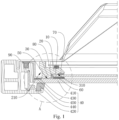
- the display device comprises a display panel 10, a middle frame 20, an annular retaining edge 30 and a cover module 40.
- the display panel 10 is mounted on a side face of the middle frame 20.
- the annular retaining edge 30 is arranged on the side face, for mounting the display panel 10, of the middle frame 20, and an inner peripheral wall of the annular retaining edge 30 is spaced from an inner peripheral wall of the middle frame 20.
- a receiving space 310 is enclosed by the annular retaining edge 30 and the middle frame 20, and the display panel 10 is limited and mounted in the receiving space 310.
- the cover module 40 comprises a protective cover 410 which covers a side, with the annular retaining edge 30, of the middle frame 20, a first buffer 60 is placed between the protective cover 410 and the display panel 10, and the protective cover 410 fixes the display panel 10 in the receiving space 310 in a pressing manner through the first buffer 60.
- the display device comprises a display panel 10, a middle frame 20, an annular retaining edge 30 and a cover module 40, an side of the middle frame 20 is provided with the annular retaining edge 30, a receiving space 310 is enclosed by the annular retaining edge 30 and the middle frame 20, the display panel 10 is limited and fixed in the receiving space 310, and the cover module 40 comprises a protective cover 410 which fixes the display panel 10 in the receiving space 310 in a pressing manner through a first buffer 60; in this way, the assembly process is simplified; because the display panel 10 is directly fixed through the protective cover 410, separate design of parts for fixing the display panel 10 is avoided, the distance between the display panel 10 and the protective cover 410 is greatly reduced, the display effect of the display device is improved, and image quality is optimized; besides, the weight and thickness of the display device are effectively reduced, and user experience is improved.
- the first buffer 60 between the protective cover 410 and the display panel 10 becomes thinner when subjected to excessive pressure. If a gap 50 between the protective cover 410 and the annular retaining edge 30 is too large, the display panel 10 may be forced out of the receiving space 310 and enter the gap 50 between the protective cover 410 and the annular retaining edge 30, and then the display panel 10 may be crushed by the protective cover 410 and the annular retaining edge 30.
- the size of the gap 50 between the protective cover 410 and the annular retaining edge 30 is smaller than the thickness of the display panel 10.
- the gap 50 is used to prevent rigid contact between the annular retaining edge 30 and the protective cover 410, and on the other hand, because the area of the middle frame 20, the annular retaining edge 30 and the protective cover 410 is large, slight deformation may occur, so the gap 50 can also provide a deformation space for the middle frame 20, the annular retaining edge 30 or the protective cover 410.
- the display panel 10 cannot leave the receiving space 310 to enter the gap 50 between the protective cover 410 and the annular retaining edge 30 in any case, so that the display panel 10 is well protected.
- the size of the gap 50 between the protective cover 410 and the annular retaining edge 30 being smaller than the thickness of the display panel 10 also makes the display panel 10 closer to the protective cover 410, thereby reducing the thickness of an air layer, so that the display effect of the display device can be improved and image quality can be optimized.
- the size of the gap 50 between the protective cover 410 and the annular retaining edge 30 is smaller than 1.5 mm.
- an air layer exists between the display panel 10 and the protective cover 410, and the thickness of the first buffer 60 in the natural state is larger than that of the air layer after the protective cover 410 is assembled, that is, after the protective cover 410 is assembled, the first buffer 60 is pressed by the display panel 10 and the protective cover 410, so that the first buffer 60 can play a sealing role to prevent external dust or water vapor from entering the air layer.
- the first buffer 60 is buffer foam, and the buffer foam is arranged along a circumferential edge of the display panel 10.
- the buffer foam is pressed by the display panel 10 and the protective cover 410 in the thickness direction, which can realize a better sealing effect and better prevent dust or water vapor from entering the air layer.
- the buffer foam has the advantages of being elastic, low in weight, capable of realizing quick pressure-sensitive fixation, convenient to use, flexible, ultra-thin, reliable in performance and so on.
- the air layer is 0.8 mm thick, and the thickness of the buffer foam needs to be greater than 0.8 mm to ensure that the buffer foam can be pressed by the display panel 10 and the protective cover 410 in the thickness direction after the cover module 40 and the middle frame 20 are assembled.
- the above-mentioned buffer foam can be bonded between the protective cover 410 and the display panel 10, or can be fixed between the protective cover 410 and the display panel 10 in a pressed mode.
- the fixing method of the buffer foam between the protective cover 410 and the display panel 10 can be determined as needed, and is not limited here.
- a second buffer 70 is arranged between the middle frame 20 and the display panel 10
- a third buffer 80 is arranged between the annular retaining edge 30 and the display panel 10.
- a side face, close to the display panel 10, of the middle frame 20 is provided with a groove for receiving the second buffer 70, and part of the second buffer 70 is locked in the groove to prevent the second buffer 70 from moving laterally between the middle frame 20 and the display panel 10 to be separated from the middle frame 20.
- the second buffer 70 and the third buffer 80 are both soft rubber or silicone strips to achieve a better buffering effect.
- the middle frame 20 and the annular retaining edge 30 are integrated with each other.
- the overall structural strength can be strengthened, and the mounting of the display device can be simplified.
- middle frame 20 may also be a combined structure formed by splicing.
- the specific structure of the middle frame 20 is determined as needed, and is not limited here.
- the cover module 40 further comprises a surface frame 420 and a cover press bar 430, the surface frame 420 surrounds and is fixed on an outer side of the middle frame 20, a stopper 421 is arranged at an opening edge, close to the display panel 10, of the surface frame 420, the cover press bar 430 is fixed to an inner peripheral wall of the surface frame 420, and cooperates with the stopper 421 to fix the protective cover 410 at an opening of the surface frame 420.
- the protective cover 410 is clamped and fixed by the surface frame 420 and the cover press bar 430, and the surface frame 420, the protective cover 410 and the cover press bar 430 are combined to form the cover module 40, so that workers can assemble the cover module 40 first, and then press the display panel 10 into the middle frame 20 through the whole cover module 40, thus improving the assembly efficiency of the display device.
- the display device further comprises a backplane 90, and the middle frame 20 and the cover module 40 are fixed on a same side face of the backplane 90.
- the surface frame 420 of the cover module 40 and the middle frame 20 are fixed on the same side face of the backplane 90, so that the surface frame 420 surrounds and is fixed on the outer side of the middle frame 20.
- the display device further comprises an optical film.
- the display panel 10 is embedded into the receiving space enclosed by the middle frame 20 and the annular retaining edge 30 while the second buffer 70 is locked in the groove of the middle frame 20 and the third buffer 80 is attached to an inner side of the annular retaining edge 30, thus completing the assembly of the display panel 10 and the middle frame 20; and the first buffer 60 is placed on an edge of the display panel 10, then the display panel 10 and the first buffer 60 are pressed inside by the whole cover module 40, and then the cover module 40 is fixedly connected with the backplane 90, thus completing the assembly of the display device.
- buffer foam is also arranged between the middle frame 20 and the optical film to prevent the middle frame 20 from scratching the optical film.
- a strip light filter 440 is arranged between the stopper 421 and the protective cover 410, and a fourth buffer 450 is arranged between the cover press bar 430 and the protective cover 410.
- the protective cover 410 of the display device generally is glass.
- both sides of the glass are not in contact with the stopper 421 and the cover press bar 430, so that the glass can be prevented from being scratched by the stopper 421 and the cover press bar 430.
- the cover module 40 further comprises an infrared plate.
- the surface frame 420 is formed by splicing four strip-shaped structures, the inside of the strip-shaped structure is provided with a locking groove in the length direction, and a surface, close to the protective cover 410, of the stopper 421 is provided with a dovetail groove or a T-shaped groove in the length direction; the infrared plate is positioned through the locking groove and inserted into the strip-shaped structure from either end of the strip-shaped structure, and the strip light filter 440 is inserted from either end of the dovetail groove or the T-shaped groove; and the four strip-shaped structures are assembled with the infrared plate and the strip light filter 440 separately. And then assembled into an integral surface frame 420.
- the cover press bar 430 comprises a pressing plate 431, a mounting plate 432 and a connecting plate 433, the pressing plate 431 and the mounting plate 432 are respectively connected to two ends of the connecting plate 433 and respectively arranged on two sides of the connecting plate 433, and the mounting plate 432 is fixed on an end face, facing away from the protective cover 410, of the surface frame 420.
- the mounting plate 432 of the cover press bar 430 is locked on an end face, facing away from the protective cover 410, of the surface frame 420 by screws, so that the cover press bar 430 can cooperate with the stopper 421 of the surface frame 420 to stably clamp the protective cover 410.
- the cover press bar 430 may be L-shaped, with a side attached to an inner side face of the surface frame 420 and locked by a screw, and another side cooperating with the stopper 421 of the surface frame 420 to clamp the protective cover 410.
- the specific structural design of the cover press bar 430 may be determined as needed, and is not limited here.
- cover press bar 430 may be designed as a whole circle or a plurality of segment structures distributed along an inner circumferential surface of the surface frame 420.
- the specific structure of the cover press bar 430 may be determined as needed, and is not limited here.
- a receding notch 210 corresponding to the cover press bar 430 is concavely formed in an outer edge of the end face, provided at the annular retaining edge 30, of the middle frame 20, a gap exists between an inner peripheral wall of the surface frame 420 and a wall surface of the receding notch 210, and the pressing plate 431 is positioned in the gap.
- the pressing plate 431 will not overlap the annular retaining edge 30 and the protective cover 410, but will be located at the outer side of the annular retaining edge 30, further reducing the thickness of the display device.
- cover press bar 430 is L-shaped, the side, attached to the inner side face of the surface frame 420, of the cover press bar 430 and the screw for locking can be placed in the gap, so as to reduce the thickness of the display device.
- the display panel 10 comprises a display area 110 in the middle and a border area 120 at the outer edges, and the buffer foam is of a split structure (usually two long and two short) and attached to the border area 120.
- the distance between the buffer foam in the border area 120 with short sides and the display area 110 is hi
- the distance between the buffer foam in the border area 120 with long sides and the display area 110 is h 2
- h 1 and h 2 are both greater than 1.5 mm, such that the display area 110 is prevented from being abraded by the buffer foam.
- the joints of the four pieces of buffer foam are tight without gaps, and the width of the buffer foam ensures that outer edges do not exceed the outer edges of the display screen after assembly.
Landscapes
- Physics & Mathematics (AREA)
- Engineering & Computer Science (AREA)
- General Physics & Mathematics (AREA)
- Nonlinear Science (AREA)
- Theoretical Computer Science (AREA)
- Optics & Photonics (AREA)
- Crystallography & Structural Chemistry (AREA)
- Chemical & Material Sciences (AREA)
- Mathematical Physics (AREA)
- Computer Hardware Design (AREA)
- Power Engineering (AREA)
- Human Computer Interaction (AREA)
- General Engineering & Computer Science (AREA)
- Devices For Indicating Variable Information By Combining Individual Elements (AREA)
Applications Claiming Priority (2)
| Application Number | Priority Date | Filing Date | Title |
|---|---|---|---|
| CN202221262300.3U CN217902627U (zh) | 2022-05-24 | 2022-05-24 | 显示设备 |
| PCT/CN2022/119878 WO2023274429A1 (fr) | 2022-05-24 | 2022-09-20 | Dispositif d'affichage |
Publications (4)
| Publication Number | Publication Date |
|---|---|
| EP4152302A1 true EP4152302A1 (fr) | 2023-03-22 |
| EP4152302A4 EP4152302A4 (fr) | 2024-06-26 |
| EP4152302B1 EP4152302B1 (fr) | 2026-01-21 |
| EP4152302C0 EP4152302C0 (fr) | 2026-01-21 |
Family
ID=84112496
Family Applications (1)
| Application Number | Title | Priority Date | Filing Date |
|---|---|---|---|
| EP22817054.4A Active EP4152302B1 (fr) | 2022-05-24 | 2022-09-20 | Dispositif d'affichage |
Country Status (5)
| Country | Link |
|---|---|
| US (1) | US12216245B2 (fr) |
| EP (1) | EP4152302B1 (fr) |
| CN (1) | CN217902627U (fr) |
| ES (1) | ES3062384T3 (fr) |
| WO (1) | WO2023274429A1 (fr) |
Families Citing this family (2)
| Publication number | Priority date | Publication date | Assignee | Title |
|---|---|---|---|---|
| CN217902627U (zh) | 2022-05-24 | 2022-11-25 | 深圳市鸿合创新信息技术有限责任公司 | 显示设备 |
| WO2024124777A1 (fr) * | 2022-12-12 | 2024-06-20 | 深圳市鸿合创新信息技术有限责任公司 | Ensemble écran d'affichage et écran d'affichage |
Family Cites Families (10)
| Publication number | Priority date | Publication date | Assignee | Title |
|---|---|---|---|---|
| JP2011002708A (ja) * | 2009-06-19 | 2011-01-06 | Sharp Corp | 表示パネルの保持構造 |
| CN208367370U (zh) * | 2018-06-20 | 2019-01-11 | 广州视源电子科技股份有限公司 | 显示装置及电子设备 |
| CN209591329U (zh) * | 2018-06-20 | 2019-11-05 | 广州视源电子科技股份有限公司 | 显示装置及电子设备 |
| CN212302156U (zh) * | 2020-05-15 | 2021-01-05 | 广州视源电子科技股份有限公司 | 显示屏及显示设备 |
| CN212433536U (zh) * | 2020-06-02 | 2021-01-29 | 广州视源电子科技股份有限公司 | 显示装置 |
| CN212460250U (zh) * | 2020-06-02 | 2021-02-02 | 广州视源电子科技股份有限公司 | 显示装置 |
| CN114442356B (zh) * | 2020-10-30 | 2024-02-23 | 高创(苏州)电子有限公司 | 显示模组及电子设备 |
| CN215932302U (zh) * | 2021-07-19 | 2022-03-01 | 广州视源电子科技股份有限公司 | 一种显示装置的膜片全贴结构、显示器及交互平板 |
| CN216351649U (zh) * | 2021-11-30 | 2022-04-19 | 深圳市鸿合创新信息技术有限责任公司 | 一种显示屏 |
| CN217902627U (zh) | 2022-05-24 | 2022-11-25 | 深圳市鸿合创新信息技术有限责任公司 | 显示设备 |
-
2022
- 2022-05-24 CN CN202221262300.3U patent/CN217902627U/zh active Active
- 2022-09-20 EP EP22817054.4A patent/EP4152302B1/fr active Active
- 2022-09-20 US US18/011,328 patent/US12216245B2/en active Active
- 2022-09-20 ES ES22817054T patent/ES3062384T3/es active Active
- 2022-09-20 WO PCT/CN2022/119878 patent/WO2023274429A1/fr not_active Ceased
Also Published As
| Publication number | Publication date |
|---|---|
| EP4152302B1 (fr) | 2026-01-21 |
| US20240118457A1 (en) | 2024-04-11 |
| EP4152302C0 (fr) | 2026-01-21 |
| US12216245B2 (en) | 2025-02-04 |
| CN217902627U (zh) | 2022-11-25 |
| EP4152302A4 (fr) | 2024-06-26 |
| WO2023274429A1 (fr) | 2023-01-05 |
| ES3062384T3 (en) | 2026-04-10 |
Similar Documents
| Publication | Publication Date | Title |
|---|---|---|
| EP4152302A1 (fr) | Dispositif d'affichage | |
| CN102237063B (zh) | 显示装置 | |
| CN101231420B (zh) | 液晶显示器件及其制造方法 | |
| US20190239375A1 (en) | Electronic device and stopping structure thereof | |
| CN111650685B (zh) | 一种显示模组及显示装置 | |
| CN211454429U (zh) | 电子设备 | |
| CN205427382U (zh) | 一种液晶显示装置 | |
| US11402570B2 (en) | Backlight module and display device | |
| WO2022083303A1 (fr) | Module d'affichage et module d'affichage monté sur véhicule | |
| TWI408442B (zh) | 液晶顯示裝置 | |
| WO2022141640A1 (fr) | Module de rétroéclairage et dispositif d'affichage | |
| WO2018205837A1 (fr) | Module de rétroéclairage et appareil d'affichage | |
| WO2018201311A1 (fr) | Module de rétroéclairage et dispositif d'affichage | |
| US7197227B2 (en) | Assembly structure of optical film and frame | |
| CN212460251U (zh) | 显示装置 | |
| KR102339645B1 (ko) | 액정표시장치 | |
| CN209657033U (zh) | 一种液晶显示装置 | |
| WO2017075954A1 (fr) | Module de rétroéclairage et dispositif d'affichage | |
| US20240169864A1 (en) | Four-sided bezel-free full screen structure | |
| CN218956970U (zh) | 一种显示屏组件及显示屏 | |
| KR100493616B1 (ko) | 액정표시장치 | |
| KR102292809B1 (ko) | 디스플레이 패널 및 그 제조 방법, 디스플레이 장치, 및 단말기 | |
| US20250085578A1 (en) | Display screen assembly and display screen | |
| CN218240599U (zh) | 一种超薄液晶显示模组 | |
| CN219039522U (zh) | 一种显示屏 |
Legal Events
| Date | Code | Title | Description |
|---|---|---|---|
| STAA | Information on the status of an ep patent application or granted ep patent |
Free format text: STATUS: UNKNOWN |
|
| STAA | Information on the status of an ep patent application or granted ep patent |
Free format text: STATUS: THE INTERNATIONAL PUBLICATION HAS BEEN MADE |
|
| PUAI | Public reference made under article 153(3) epc to a published international application that has entered the european phase |
Free format text: ORIGINAL CODE: 0009012 |
|
| STAA | Information on the status of an ep patent application or granted ep patent |
Free format text: STATUS: REQUEST FOR EXAMINATION WAS MADE |
|
| 17P | Request for examination filed |
Effective date: 20221212 |
|
| AK | Designated contracting states |
Kind code of ref document: A1 Designated state(s): AL AT BE BG CH CY CZ DE DK EE ES FI FR GB GR HR HU IE IS IT LI LT LU LV MC MK MT NL NO PL PT RO RS SE SI SK SM TR |
|
| A4 | Supplementary search report drawn up and despatched |
Effective date: 20240529 |
|
| RIC1 | Information provided on ipc code assigned before grant |
Ipc: H05K 5/03 20060101ALI20240523BHEP Ipc: H05K 5/02 20060101ALI20240523BHEP Ipc: G09F 9/00 20060101AFI20240523BHEP |
|
| DAV | Request for validation of the european patent (deleted) | ||
| DAX | Request for extension of the european patent (deleted) | ||
| GRAP | Despatch of communication of intention to grant a patent |
Free format text: ORIGINAL CODE: EPIDOSNIGR1 |
|
| STAA | Information on the status of an ep patent application or granted ep patent |
Free format text: STATUS: GRANT OF PATENT IS INTENDED |
|
| INTG | Intention to grant announced |
Effective date: 20251029 |
|
| GRAS | Grant fee paid |
Free format text: ORIGINAL CODE: EPIDOSNIGR3 |
|
| GRAA | (expected) grant |
Free format text: ORIGINAL CODE: 0009210 |
|
| STAA | Information on the status of an ep patent application or granted ep patent |
Free format text: STATUS: THE PATENT HAS BEEN GRANTED |
|
| AK | Designated contracting states |
Kind code of ref document: B1 Designated state(s): AL AT BE BG CH CY CZ DE DK EE ES FI FR GB GR HR HU IE IS IT LI LT LU LV MC MK MT NL NO PL PT RO RS SE SI SK SM TR |
|
| REG | Reference to a national code |
Ref country code: CH Ref legal event code: F10 Free format text: ST27 STATUS EVENT CODE: U-0-0-F10-F00 (AS PROVIDED BY THE NATIONAL OFFICE) Effective date: 20260121 |
|
| REG | Reference to a national code |
Ref country code: DE Ref legal event code: R096 Ref document number: 602022028955 Country of ref document: DE |
|
| REG | Reference to a national code |
Ref country code: IE Ref legal event code: FG4D |
|
| U01 | Request for unitary effect filed |
Effective date: 20260223 |
|
| U07 | Unitary effect registered |
Designated state(s): AT BE BG DE DK EE FI FR IT LT LU LV MT NL PT RO SE SI Effective date: 20260226 |
|
| REG | Reference to a national code |
Ref country code: ES Ref legal event code: FG2A Ref document number: 3062384 Country of ref document: ES Kind code of ref document: T3 Effective date: 20260410 |