EP4155255A1 - Verfahren zur herstellung einer mikroelektromechanischen vorrichtung aus einem einzigen halbleiter-wafer und zugehörige mems-vorrichtung - Google Patents
Verfahren zur herstellung einer mikroelektromechanischen vorrichtung aus einem einzigen halbleiter-wafer und zugehörige mems-vorrichtung Download PDFInfo
- Publication number
- EP4155255A1 EP4155255A1 EP22195564.4A EP22195564A EP4155255A1 EP 4155255 A1 EP4155255 A1 EP 4155255A1 EP 22195564 A EP22195564 A EP 22195564A EP 4155255 A1 EP4155255 A1 EP 4155255A1
- Authority
- EP
- European Patent Office
- Prior art keywords
- layer
- region
- forming
- ceiling
- openings
- Prior art date
- Legal status (The legal status is an assumption and is not a legal conclusion. Google has not performed a legal analysis and makes no representation as to the accuracy of the status listed.)
- Granted
Links
Images


Classifications
-
- B—PERFORMING OPERATIONS; TRANSPORTING
- B81—MICROSTRUCTURAL TECHNOLOGY
- B81C—PROCESSES OR APPARATUS SPECIALLY ADAPTED FOR THE MANUFACTURE OR TREATMENT OF MICROSTRUCTURAL DEVICES OR SYSTEMS
- B81C1/00—Manufacture or treatment of devices or systems in or on a substrate
- B81C1/00015—Manufacture or treatment of devices or systems in or on a substrate for manufacturing microsystems
- B81C1/00261—Processes for packaging MEMS devices
- B81C1/00333—Aspects relating to packaging of MEMS devices, not covered by groups B81C1/00269 - B81C1/00325
-
- B—PERFORMING OPERATIONS; TRANSPORTING
- B81—MICROSTRUCTURAL TECHNOLOGY
- B81C—PROCESSES OR APPARATUS SPECIALLY ADAPTED FOR THE MANUFACTURE OR TREATMENT OF MICROSTRUCTURAL DEVICES OR SYSTEMS
- B81C1/00—Manufacture or treatment of devices or systems in or on a substrate
- B81C1/00015—Manufacture or treatment of devices or systems in or on a substrate for manufacturing microsystems
- B81C1/00134—Manufacture or treatment of devices or systems in or on a substrate for manufacturing microsystems comprising flexible or deformable structures
- B81C1/00182—Arrangements of deformable or non-deformable structures, e.g. membrane and cavity for use in a transducer
-
- B—PERFORMING OPERATIONS; TRANSPORTING
- B81—MICROSTRUCTURAL TECHNOLOGY
- B81B—MICROSTRUCTURAL DEVICES OR SYSTEMS, e.g. MICROMECHANICAL DEVICES
- B81B3/00—Devices comprising flexible or deformable elements, e.g. comprising elastic tongues or membranes
- B81B3/0018—Structures acting upon the moving or flexible element for transforming energy into mechanical movement or vice versa, i.e. actuators, sensors, generators
- B81B3/0032—Structures for transforming energy not provided for in groups B81B3/0021 - B81B3/0029
-
- B—PERFORMING OPERATIONS; TRANSPORTING
- B81—MICROSTRUCTURAL TECHNOLOGY
- B81C—PROCESSES OR APPARATUS SPECIALLY ADAPTED FOR THE MANUFACTURE OR TREATMENT OF MICROSTRUCTURAL DEVICES OR SYSTEMS
- B81C1/00—Manufacture or treatment of devices or systems in or on a substrate
- B81C1/00436—Shaping materials, i.e. techniques for structuring the substrate or the layers on the substrate
- B81C1/00444—Surface micromachining, i.e. structuring layers on the substrate
- B81C1/00468—Releasing structures
- B81C1/00476—Releasing structures removing a sacrificial layer
-
- B—PERFORMING OPERATIONS; TRANSPORTING
- B81—MICROSTRUCTURAL TECHNOLOGY
- B81B—MICROSTRUCTURAL DEVICES OR SYSTEMS, e.g. MICROMECHANICAL DEVICES
- B81B2201/00—Specific applications of microelectromechanical systems
- B81B2201/02—Sensors
- B81B2201/0221—Variable capacitors
-
- B—PERFORMING OPERATIONS; TRANSPORTING
- B81—MICROSTRUCTURAL TECHNOLOGY
- B81B—MICROSTRUCTURAL DEVICES OR SYSTEMS, e.g. MICROMECHANICAL DEVICES
- B81B2201/00—Specific applications of microelectromechanical systems
- B81B2201/02—Sensors
- B81B2201/0228—Inertial sensors
- B81B2201/0235—Accelerometers
-
- B—PERFORMING OPERATIONS; TRANSPORTING
- B81—MICROSTRUCTURAL TECHNOLOGY
- B81B—MICROSTRUCTURAL DEVICES OR SYSTEMS, e.g. MICROMECHANICAL DEVICES
- B81B2201/00—Specific applications of microelectromechanical systems
- B81B2201/02—Sensors
- B81B2201/0228—Inertial sensors
- B81B2201/0242—Gyroscopes
-
- B—PERFORMING OPERATIONS; TRANSPORTING
- B81—MICROSTRUCTURAL TECHNOLOGY
- B81B—MICROSTRUCTURAL DEVICES OR SYSTEMS, e.g. MICROMECHANICAL DEVICES
- B81B2203/00—Basic microelectromechanical structures
- B81B2203/05—Type of movement
- B81B2203/055—Translation in a plane parallel to the substrate, i.e. enabling movement along any direction in the plane
-
- B—PERFORMING OPERATIONS; TRANSPORTING
- B81—MICROSTRUCTURAL TECHNOLOGY
- B81B—MICROSTRUCTURAL DEVICES OR SYSTEMS, e.g. MICROMECHANICAL DEVICES
- B81B2207/00—Microstructural systems or auxiliary parts thereof
- B81B2207/11—Structural features, others than packages, for protecting a device against environmental influences
- B81B2207/115—Protective layers applied directly to the device before packaging
-
- B—PERFORMING OPERATIONS; TRANSPORTING
- B81—MICROSTRUCTURAL TECHNOLOGY
- B81C—PROCESSES OR APPARATUS SPECIALLY ADAPTED FOR THE MANUFACTURE OR TREATMENT OF MICROSTRUCTURAL DEVICES OR SYSTEMS
- B81C2201/00—Manufacture or treatment of microstructural devices or systems
- B81C2201/01—Manufacture or treatment of microstructural devices or systems in or on a substrate
- B81C2201/0101—Shaping material; Structuring the bulk substrate or layers on the substrate; Film patterning
- B81C2201/0102—Surface micromachining
- B81C2201/0105—Sacrificial layer
- B81C2201/0109—Sacrificial layers not provided for in B81C2201/0107 - B81C2201/0108
-
- B—PERFORMING OPERATIONS; TRANSPORTING
- B81—MICROSTRUCTURAL TECHNOLOGY
- B81C—PROCESSES OR APPARATUS SPECIALLY ADAPTED FOR THE MANUFACTURE OR TREATMENT OF MICROSTRUCTURAL DEVICES OR SYSTEMS
- B81C2201/00—Manufacture or treatment of microstructural devices or systems
- B81C2201/01—Manufacture or treatment of microstructural devices or systems in or on a substrate
- B81C2201/0101—Shaping material; Structuring the bulk substrate or layers on the substrate; Film patterning
- B81C2201/0128—Processes for removing material
- B81C2201/013—Etching
- B81C2201/0132—Dry etching, i.e. plasma etching, barrel etching, reactive ion etching [RIE], sputter etching or ion milling
-
- B—PERFORMING OPERATIONS; TRANSPORTING
- B81—MICROSTRUCTURAL TECHNOLOGY
- B81C—PROCESSES OR APPARATUS SPECIALLY ADAPTED FOR THE MANUFACTURE OR TREATMENT OF MICROSTRUCTURAL DEVICES OR SYSTEMS
- B81C2201/00—Manufacture or treatment of microstructural devices or systems
- B81C2201/01—Manufacture or treatment of microstructural devices or systems in or on a substrate
- B81C2201/0174—Manufacture or treatment of microstructural devices or systems in or on a substrate for making multi-layered devices, film deposition or growing
- B81C2201/0176—Chemical vapour Deposition
Definitions
- the present invention relates to a process for manufacturing a MEMS (Micro-Electro-Mechanical System) device from a single semiconductor wafer, as well as to the related MEMS device.
- MEMS Micro-Electro-Mechanical System
- MEMS accelerometers are, for example, today available, which enable, for example, measurement of linear accelerations, inclinations and vibrations.
- These MEMS accelerometers generally comprise a vacuum cavity, isolated from the surrounding environment. The production of this cavity proves problematical.
- the cavity is formed by bonding together a cap wafer and a device wafer; for example, a glassfrit bonding or a metal-bonding can be carried out, however, both of the solutions present some disadvantages, in addition to requiring the use of two patterned wafers.
- both solutions are characterized by a low uniformity of the quality factor of the accelerometers produced, on account of the non-uniformity deriving from the process of bonding of the two wafers.
- glassfrit printing presents high tolerances, which entails a reduction of the useful area for the formation of the accelerometers.
- the cap wafer must be patterned so as to accommodate deformation of the glassfrit paste during bonding, with consequent increase in the final size of the accelerometers produced.
- the use of a lead paste is required, a material that is potentially dangerous for health.
- metal bonding it is necessary to pattern metal regions both on the cap wafer and on the device wafer, as well as to carry out cleaning steps before performing the bonding. Furthermore, the bonding is carried out at temperatures close to 400°C and with high bonding forces, which may lead to chipping of the metal regions. In both cases, the production cost is high on account of the use of a second silicon wafer.
- US US2009/267166 A1 discloses a method for manufacturing a micro-device, comprising: providing a substrate having a surface, with a sacrificial oxide region arranged on the surface; covering the sacrificial oxide region with a porous layer permeable to the gaseous hydrofluoric acid; and selectively etching the sacrificial oxide region through the porous layer using the gaseous hydrofluoric acid, to obtain a cavity.
- the aim of the present invention is consequently to provide a solution that will overcome at least in part the drawbacks of the prior art.
- the MEMS device may be an accelerometer, a gyroscope, an inclinometer or an actuator. Furthermore, it is assumed, for example, that the MEMS device is of the type with control/detection of a capacitive type.
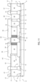
- the present process initially envisages forming an insulating region 4 on a substrate 6 of a semiconductor wafer 8; the substrate 6 is made of semiconductor material, such as, for example, silicon.
- the insulating region 4 may be made of subregions of different materials, such as, for example, a subregion of thermal oxide, arranged on the substrate 6, and an overlying subregion of thermally stabilised aluminium oxide. Furthermore, hereinafter the present description is limited to the evolution of a portion of the semiconductor wafer 8 that gives rise to a single MEMS device.
- portions of the insulating region 4 are selectively removed so as to form recesses 9 that give out onto the underlying substrate 6.
- a conductive stator region 10 and a conductive rotor region 12 are formed on the insulating region 4, which are laterally staggered and extend, not only over the insulating region 4, but also within respective recesses 9 so as to contact corresponding portions of the substrate 6. Furthermore, an additional conductive region 14 is also formed, which extends over a corresponding portion of the insulating region 4, is separated from the substrate 6, and is laterally staggered with respect to the conductive stator region 10 and to the conductive rotor region 12.
- the conductive stator region 10, the conductive rotor region 12, and the additional conductive region 14 may be formed, for example, by deposition, on the insulating region 4 and within the recesses 9, of a polysilicon layer with a high doping level (for example, of an N type), also known as polyrunner, and subsequent patterning such that the conductive stator region 10, the conductive rotor region 12, and the additional conductive region 14 are electrically separated from one another.
- a polysilicon layer with a high doping level for example, of an N type
- Figure 3 refers to the case in which the conductive stator region 10 has a closed and hollow shape, in top view, such as, for example, the shape of a frame or annulus, and surrounds, once again in top view, the conductive rotor region 12.
- a first sacrificial region 15 is formed, on the insulating region 4, the conductive stator region 10, the conductive rotor region 12, and the additional conductive region 14.
- the first sacrificial region 15 is made of dielectric material, such as, for example, TEOS oxide.
- portions of the first sacrificial region 15 and of the insulating region 4 are selectively removed so as to form a trench 17, which has a closed profile, in top view, and extends through the first sacrificial region 15 and the insulating region 4 so as to be delimited at the bottom by a corresponding exposed portion of the substrate 6. Furthermore, portions of the first sacrificial region 15 are selectively removed so as to form a stator window 19, a rotor window 21, and a buttress window 23, which traverse the first sacrificial region 15 and give out, respectively, onto the conductive stator region 10, onto the conductive rotor region 12, and onto the additional conductive region 14 so as to expose corresponding portions of these regions.
- the trench 17 may be formed by carrying out an etch different from the etch that leads to formation of the stator window 19, the rotor window 21, and the buttress window 23; i.e., two different masks may be used.
- the trench 17, the stator window 19, the rotor window 21, and the buttress window 23 form a sort of plurality of preliminary windows.
- a first deposition of silicon is carried out so as to form a structural layer 25 of polycrystalline silicon, for example with a doping of an N type and having a thickness comprised, for example, between 15 ⁇ m and 60 ⁇ m.
- the structural layer 25 extends, in direct contact, over the first sacrificial region 15, as well as within the trench 17, the stator window 19, the rotor window 21, and the buttress window 23 so as to contact the substrate 6, the conductive stator region 10, the conductive rotor region 12, and the additional conductive region 14.
- the structural layer 25 may also undergo chemical-mechanical planarization (CMP).
- the structural layer 25 is formed on a base region of the semiconductor wafer 8, which includes the substrate 6, the insulating region 4, the conductive stator region 10, the conductive rotor region 12, the additional conductive region 14, and the first sacrificial region 15.
- an insulating layer 27 formed, for example, of silicon nitride (SiN), which, as illustrated in Figure 8 , is then patterned so as to form a first, a second and a third electrical-decoupling region 31, 32, 33, laterally staggered with respect to one another.
- SiN silicon nitride
- the first electrical-decoupling region 31 overlies, at a distance, the trench 17.
- the second and the third electrical-decoupling regions 32, 33 overlie, at a distance, a part of the stator window 19 and the rotor window 21, respectively.
- the first, the second and the third electrical-decoupling regions 31, 32, 33 are laterally staggered with respect to the buttress window 23.
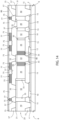
- first openings 35 extend through the structural layer 25 and are delimited at the bottom by corresponding portions of the first sacrificial region 15. Furthermore, for reasons that will be clarified hereinafter, the first openings 35 may have a so-called critical dimension (CD); for example, this will not exceed 4 ⁇ m.
- CD critical dimension
- the first openings 35 laterally delimit portions of the structural layer 25 that form, respectively, a perimetral region 40, a fixed stator region 42, a mobile mass 44, a first and a second spring 46, 48, a preliminary buttress region 49, and a pillar region 50.
- the fixed stator region 42 extends in the stator window 19 and overlies, in direct contact, the conductive stator region 10. Furthermore, the fixed stator region 42 laterally surrounds the mobile mass 44, the first and the second springs 46, 48, and the pillar region 50. Part of the fixed stator region 42 is overlaid by the second electrical-decoupling region 32.
- the mobile mass 44 is laterally staggered with respect to the first, the second and the third electrical-decoupling regions 31, 32, 33; therefore, it is exposed at the top. Furthermore, the mobile mass 44 overlies a portion of the first sacrificial region 15 and, albeit not illustrated, has a hollow shape (for example, it has the shape of a rectangular frame or annulus, in top view) so as to surround laterally the pillar region 50.
- the pillar region 50 extends underneath the third electrical-decoupling region 33. Furthermore, the pillar region 50 extends within the rotor window 21 so as to contact the conductive rotor region 12.
- the mobile mass 44 is mechanically coupled to the pillar region 50 by the first and the second springs 46, 48, each of which is interposed between the mobile mass 44 and the pillar region 50.
- the first and the second springs 46, 48 are arranged in a symmetrical way with respect to the pillar region 50.
- first and the second springs 46, 48 are laterally staggered with respect to the first, the second and the third electrical-decoupling regions 31, 32, 33, and are therefore exposed at the top.
- first and the second springs 46, 48 overlie, in direct contact, the first sacrificial region 15. Once released, the first and the second springs 46, 48 are deformable so as to enable the mobile mass 44 to translate in a plane parallel to the main surface of the substrate 6 of the semiconductor wafer 8, as explained hereinafter.
- the perimetral region 40 extends underneath the first electrical-decoupling region 31. Furthermore, the perimetral region 40 extends in the trench 17 so as to contact the substrate 6. Furthermore, the perimetral region 40 laterally surrounds the fixed stator region 42 and the preliminary buttress region 49.
- the preliminary buttress region 49 is laterally staggered with respect to the first, the second and the third electrical-decoupling regions 31, 32, 33, and is therefore exposed at the top. Furthermore, the preliminary buttress region 49 extends in the buttress window 23 so as to contact the additional conductive region 14. In addition, the preliminary buttress region 49 is interposed, at a distance, between the fixed stator region 42 and the perimetral region 40.
- a first dielectric covering region 54 is formed, which is formed, for example, by performing one or more depositions of oxide (for example, silicon oxide obtained by TEOS-based chemical vapour deposition, CVD) followed by CMP.
- oxide for example, silicon oxide obtained by TEOS-based chemical vapour deposition, CVD
- CMP chemical vapour deposition
- the first dielectric covering region 54 overlies, in direct contact, the first, the second and the third electrical-decoupling regions 31, 32, 33, as well as the exposed portions of the structural layer 25, and therefore the exposed part of the fixed stator region 42, the mobile mass 44, the first and the second springs 46, 48 and the preliminary buttress region 49.
- the first dielectric covering region 54 closes the first openings 35 at the top, for example without filling them completely.
- a second dielectric covering region 56 is formed on the first dielectric covering region 54, for example by deposition of oxide (for example, silicon oxide obtained from TEOS-based CVD).
- oxide for example, silicon oxide obtained from TEOS-based CVD.
- the first and the second dielectric covering regions 54, 56 are illustrated as distinct, they may be made of a same material so as to form a single second sacrificial region 57.
- the second sacrificial region 57 will be shown as a whole.
- the second dielectric covering region 56 is machined (for example, by execution of a selective timed etch of a dry type) so as to form the surface grooves 58.
- portions of the second sacrificial region 57 are selectively removed so as to form an anchorage rotor window 60, a perimetral anchorage window 61, an anchorage stator window 62, and an anchorage buttress window 69.
- the perimetral anchorage window 61 traverses the second sacrificial region 57 and gives out onto the first electrical-decoupling region 31.
- the anchorage stator window 62 traverses the second sacrificial region 57 and gives out onto the second electrical-decoupling region 32.
- the anchorage rotor window 60 traverses the second sacrificial region 57 and gives out onto the third electrical-decoupling region 33.
- the anchorage buttress window 69 traverses the second sacrificial region 57 and gives out onto the preliminary buttress region 49.
- the anchorage buttress window 69, the anchorage rotor window 60, the perimetral anchorage window 61, and the anchorage stator window 62 may be formed during a same etching operation, thus using a single mask.
- a second deposition of silicon is performed so as to form a ceiling layer 75 of polycrystalline silicon, for example, with a doping of an N type and having a thickness comprised, for example, between 5 ⁇ m and 10 ⁇ m.
- a subsequent planarization of the ceiling layer 75 is also carried out.
- the ceiling layer 75 extends, in direct contact, over the second sacrificial region 57. Furthermore, portions of the ceiling layer 75 extend respectively within the anchorage rotor window 60, the perimetral anchorage window 61, the anchorage stator window 62, and the anchorage buttress window 69 so as to contact the first, the second and the third electrical-decoupling regions 31, 32, 33, as well as the preliminary buttress region 49. In this connection, the ceiling layer 75 forms, with the preliminary buttress region 49, a single semiconductor region (for reasons of clarity, in Figure 12 and in the subsequent figures the line of demarcation between the ceiling layer 75 and the preliminary buttress region 49 is in any case maintained). In addition, the ceiling layer 75 fills the grooves 58.
- portions of the ceiling layer 75 are selectively removed by carrying out a dry etch so as to form a plurality of second openings 77, which give out onto corresponding portions of the second sacrificial region 57.
- the second openings 77 may have a critical dimension, for example, not exceeding 1 ⁇ m.
- a layer 80 of polysilicon permeable to hydrofluoric acid (HF) is deposited on the ceiling layer 75; hereinafter the layer 80 is referred to as the permeable layer 80.
- the permeable layer 80 closes the second openings 77 at the top, for example without filling them completely.
- the permeable layer 80 has a thickness comprised, for example, between 70 nm and 200 nm and is formed by low pressure chemical vapour deposition (LPCVD), using silane (SiH 4 ) as precursor, with a pressure comprised, for example, between 100 mTorr and 1000 mTorr and with a temperature comprised, for example, between 580°C and 640°C.
- LPCVD low pressure chemical vapour deposition
- SiH 4 silane
- the permeable layer 80 has a porous structure, permeable to gaseous hydrofluoric acid.
- the first and the second sacrificial regions 15, 57 are selectively removed, thus causing the hydrofluoric acid in the gaseous phase to flow through the permeable layer 80 and the second openings 77.
- the hydrofluoric acid traverses the first openings 35 and causes removal of the first sacrificial region 15. In this way, as illustrated in Figure 15 , there occurs release of the mobile mass 44 and of the first and the second springs 46, 48.
- the hydrofluoric acid etches the dielectric material that forms the first and the second sacrificial regions 15, 57, but substantially does not etch the polysilicon, nor the insulating region 4.
- the insulating region 4 is not etched by the hydrofluoric acid thanks to the presence of the thermally stabilised aluminium oxide.
- the hydrofluoric acid does not etch the silicon nitride that forms the first, the second and the third electrical-decoupling regions 31, 32, 33.
- the spaces previously occupied by the first and the second sacrificial regions 15, 57 form, together with the first openings 35, a cavity 99, which is laterally delimited by the perimetral region 40, the first electrical-decoupling region 31, and the portion of the ceiling layer 75 that contacts the latter.
- the first electrical-decoupling region 31 enables electrical insulation of the perimetral region 40 from the ceiling layer 75.
- the cavity 99 is also delimited at the top by the ceiling layer 75 and is in fluidic communication with the overlying second openings 77.
- the cavity 99 is also delimited at the bottom by the insulating region 4.
- Extending within the cavity 99 are the fixed stator region 42, the mobile mass 44, the first and the second springs 46, 48, the preliminary buttress region 49, and the pillar region 50.
- the mobile mass 44 and the first and the second springs 46, 48 are suspended within the cavity 99.
- the parts of the ceiling layer 75 that previously occupied the grooves 58 function as so-called Z stoppers for the mobile mass 44.
- the fixed stator region 42 is fixed to the ceiling layer 75 by interposition of the first electrical-decoupling region 31; the pillar region 50 is fixed to the ceiling layer 75 by interposition of the third electrical-decoupling region 33.
- the fixed stator region 42 and the pillar region 50 are in any case electrically insulated from the ceiling layer 75.
- a third deposition of silicon is carried out so as to form, on the permeable layer 80, a sealing layer 95 of polycrystalline silicon, for example having a doping of an N type and having a thickness comprised, for example, between 2 ⁇ m and 50 ⁇ m.
- the sealing layer 95 may also undergo planarization.
- the sealing layer 95 may be formed by deposition in an environment at a controlled pressure (for example, comprised between 0.1 bar and 1 bar) and with a temperature comprised between 800°C and 1200°C. Furthermore, optionally a process of degassing may be carried out in order to enable the hydrogen present in the cavity 99 to diffuse through the sealing layer 95 so as to cause the cavity 99 to be approximately in vacuum conditions or in any case to present a desired pressure therein.
- a controlled pressure for example, comprised between 0.1 bar and 1 bar
- a temperature comprised between 800°C and 1200°C.
- a process of degassing may be carried out in order to enable the hydrogen present in the cavity 99 to diffuse through the sealing layer 95 so as to cause the cavity 99 to be approximately in vacuum conditions or in any case to present a desired pressure therein.
- the deposition process of the sealing layer 95 also causes a variation of permeability of the permeable layer 80.
- the previously porous structure of the permeable layer 80 undergoes filling, such that the permeable layer 80 loses the previous characteristic of permeability and assumes a crystalline structure approximately similar to that of the sealing layer 95 and to that of the ceiling layer 75, but with grains on average smaller than the grains of the crystalline structures of the sealing layer 95 and of the ceiling layer 75.
- the permeable layer 80 as transformed following upon formation of the sealing layer 95 is referred to as the transformed layer 180.
- an interface i.e., a discontinuity in the crystalline structure, is therefore present between the transformed layer 180 and the sealing layer 95.
- another interface is present between the transformed layer 180 and the ceiling layer 75.
- the sealing layer 95 and the transformed layer 180 provide hermetic sealing of the second openings 77; i.e., they seal at the top the ensemble formed by the cavity 99 and the second openings 77, which is moreover hermetically closed thanks to the mechanical coupling present between the ceiling layer 75 and the perimetral region 40, as well as thanks to the mechanical coupling present between the perimetral region 40 and the substrate 6.
- the preliminary buttress region 49 forms, together with the overlying portion of the ceiling layer 75, a buttress structure, which has the function of locally propping the ensemble formed by the ceiling layer 75, the transformed layer 180 and the sealing layer 95 so as to increase the stiffness thereof in order to prevent deformation (for example, bending) thereof.
- the arrangement and shape of the buttress structure may be optimised, for example according to the arrangement and shape of the fixed stator region 42, the mobile mass 44 and the pillar region 50.
- the manufacturing process envisages two possible variants.
- the semiconductor wafer 8 is flipped over and the substrate 6 is then machined so as to form at least a first and a second through silicon via 96, 98; furthermore, a stator metallization 100 and a rotor metallization 102 are formed, these metallizations being arranged on the main surface of the substrate 6 opposite to the insulating region 4. Furthermore, the first through silicon via 96 electrically connects the stator metallization 100 to the conductive stator region 10, while the second through silicon via 98 electrically connects the rotor metallization 102 to the conductive rotor region 12.
- the manufacturing process may proceed in a per se known manner, for example, by forming further passivation regions and contact pads (not illustrated). Furthermore, a process of dicing of the semiconductor wafer 8 is then carried out, for example, along scribe lines CL that traverse the perimetral region 40 (illustrated in Figure 17 ) so as to singulate a plurality of MEMS devices (one of which is illustrated in Figure 17 , where it is designated by 101).
- the semiconductor wafer 8 after being flipped over, is temporarily bonded to a supporting wafer 120, by using an adhesive layer 122, which is interposed between the sealing layer 95 and the supporting wafer 120.
- the thickness of the substrate 6 is reduced by a so-called lapping and polishing process.
- the first and the second through silicon vias 96, 98 are formed after the stator metallization 100 and the rotor metallization 102 have been formed. Then, the manufacturing process proceeds in the same way as described with reference to the first variant.
- this second variant enables MEMS devices to be obtained having a further reduced final thickness (for example, less than 300 ⁇ m) as compared to what can be obtained with the first variant.
- the present solution enables reduction of the manufacturing costs, since it envisages the use of a single wafer. Furthermore, the present solution enables reduction of the dimensions (in particular, the thickness) of the MEMS device.
- the present solution affords a better uniformity of the quality factor of the MEMS devices produced since it does not entail implementation of a wafer-bonding process.
- the present solution also does not entail the use of lead-containing compounds, such as, for example, glassfrit paste.
- the MEMS device may be of the type with control/detection of a non-capacitive type (for example, piezoelectric).
- a non-capacitive type for example, piezoelectric
- the functional elements understood as mobile and/or deformable elements
- the MEMS device it is possible for the MEMS device to have a different type of functional elements (for example, cantilever elements), mobile within the cavity 99, which may again be hermetically closed.
- semiconductor regions are present that function, for example, as anode and cathode.
- Removal of the first and the second sacrificial regions 15, 57 may be partial.
- the buttress structure, and therefore the preliminary buttress structure 49, may be absent, as likewise the additional conductive region 14.
Landscapes
- Engineering & Computer Science (AREA)
- Microelectronics & Electronic Packaging (AREA)
- Manufacturing & Machinery (AREA)
- Chemical & Material Sciences (AREA)
- Analytical Chemistry (AREA)
- Computer Hardware Design (AREA)
- Micromachines (AREA)
Applications Claiming Priority (1)
| Application Number | Priority Date | Filing Date | Title |
|---|---|---|---|
| IT102021000024785A IT202100024785A1 (it) | 2021-09-28 | 2021-09-28 | Procedimento di fabbricazione di un dispositivo micro-elettro-meccanico a partire da una singola fetta semiconduttiva e relativo dispositivo mems |
Publications (2)
| Publication Number | Publication Date |
|---|---|
| EP4155255A1 true EP4155255A1 (de) | 2023-03-29 |
| EP4155255B1 EP4155255B1 (de) | 2025-09-10 |
Family
ID=78771080
Family Applications (1)
| Application Number | Title | Priority Date | Filing Date |
|---|---|---|---|
| EP22195564.4A Active EP4155255B1 (de) | 2021-09-28 | 2022-09-14 | Verfahren zur herstellung einer mikroelektromechanischen vorrichtung aus einem einzigen halbleiter-wafer und zugehörige mems-vorrichtung |
Country Status (3)
| Country | Link |
|---|---|
| US (1) | US12589989B2 (de) |
| EP (1) | EP4155255B1 (de) |
| IT (1) | IT202100024785A1 (de) |
Citations (1)
| Publication number | Priority date | Publication date | Assignee | Title |
|---|---|---|---|---|
| US20090267166A1 (en) | 2008-04-23 | 2009-10-29 | Taiwan Semiconductor Manufacturing Company, Ltd. | Method of manufacturing a device with a cavity |
Family Cites Families (5)
| Publication number | Priority date | Publication date | Assignee | Title |
|---|---|---|---|---|
| DE10024697B4 (de) * | 2000-05-18 | 2008-08-21 | Robert Bosch Gmbh | Mikromechanisches Bauelement und entsprechendes Herstellungsverfahren |
| DE10352001A1 (de) * | 2003-11-07 | 2005-06-09 | Robert Bosch Gmbh | Mikromechanisches Bauelement mit einer Membran und Verfahren zur Herstellung eines solchen Bauelements |
| JP6034619B2 (ja) * | 2011-08-22 | 2016-11-30 | パナソニック株式会社 | Mems素子およびそれを用いた電気機器 |
| US9932224B2 (en) * | 2015-12-17 | 2018-04-03 | Globalfoundries Singapore Pte. Ltd. | Semiconductor devices with cavities and methods for fabricating semiconductor devices with cavities |
| US11667516B2 (en) * | 2019-06-26 | 2023-06-06 | Qorvo Us, Inc. | MEMS device having uniform contacts |
-
2021
- 2021-09-28 IT IT102021000024785A patent/IT202100024785A1/it unknown
-
2022
- 2022-09-14 EP EP22195564.4A patent/EP4155255B1/de active Active
- 2022-09-19 US US17/933,439 patent/US12589989B2/en active Active
Patent Citations (1)
| Publication number | Priority date | Publication date | Assignee | Title |
|---|---|---|---|---|
| US20090267166A1 (en) | 2008-04-23 | 2009-10-29 | Taiwan Semiconductor Manufacturing Company, Ltd. | Method of manufacturing a device with a cavity |
Also Published As
| Publication number | Publication date |
|---|---|
| US20230107094A1 (en) | 2023-04-06 |
| US12589989B2 (en) | 2026-03-31 |
| IT202100024785A1 (it) | 2023-03-28 |
| EP4155255B1 (de) | 2025-09-10 |
Similar Documents
| Publication | Publication Date | Title |
|---|---|---|
| US7153718B2 (en) | Micromechanical component as well as a method for producing a micromechanical component | |
| US7579206B2 (en) | Anchors for microelectromechanical systems having an SOI substrate, and method of fabricating same | |
| US7115436B2 (en) | Integrated getter area for wafer level encapsulated microelectromechanical systems | |
| CN103373695B (zh) | Mems器件结构及其形成方法 | |
| US11697588B2 (en) | Structure for microelectromechanical systems (MEMS) devices to control pressure at high temperature | |
| CN102398888A (zh) | 晶圆级封装 | |
| US9487391B2 (en) | Micro-electro mechanical system (MEMS) device having a blocking layer formed between closed chamber and a dielectric layer of a CMOS substrate | |
| US20110210435A1 (en) | Mems devices | |
| EP4620900A1 (de) | Mems-vorrichtung und herstellungsverfahren dafür | |
| EP4155255B1 (de) | Verfahren zur herstellung einer mikroelektromechanischen vorrichtung aus einem einzigen halbleiter-wafer und zugehörige mems-vorrichtung | |
| CN218860329U (zh) | 微机电系统装置 | |
| US12017909B2 (en) | Fabrication method for a MEMS device | |
| US7531229B2 (en) | Microstructured component and method for its manufacture | |
| US12441604B2 (en) | Micro-electromechanical systems (MEMS) device with outgas layer | |
| JP2007253265A (ja) | 電気機械素子の製造方法 | |
| KR100249790B1 (ko) | 멤즈 소자의 제조 방법 | |
| WO2002091439A9 (en) | Fabrication of a microelectromechanical system (mems) device | |
| KR100236934B1 (ko) | 멤즈 소자의 형성 방법 |
Legal Events
| Date | Code | Title | Description |
|---|---|---|---|
| PUAI | Public reference made under article 153(3) epc to a published international application that has entered the european phase |
Free format text: ORIGINAL CODE: 0009012 |
|
| STAA | Information on the status of an ep patent application or granted ep patent |
Free format text: STATUS: THE APPLICATION HAS BEEN PUBLISHED |
|
| AK | Designated contracting states |
Kind code of ref document: A1 Designated state(s): AL AT BE BG CH CY CZ DE DK EE ES FI FR GB GR HR HU IE IS IT LI LT LU LV MC MK MT NL NO PL PT RO RS SE SI SK SM TR |
|
| STAA | Information on the status of an ep patent application or granted ep patent |
Free format text: STATUS: REQUEST FOR EXAMINATION WAS MADE |
|
| 17P | Request for examination filed |
Effective date: 20230925 |
|
| RBV | Designated contracting states (corrected) |
Designated state(s): AL AT BE BG CH CY CZ DE DK EE ES FI FR GB GR HR HU IE IS IT LI LT LU LV MC MK MT NL NO PL PT RO RS SE SI SK SM TR |
|
| GRAP | Despatch of communication of intention to grant a patent |
Free format text: ORIGINAL CODE: EPIDOSNIGR1 |
|
| STAA | Information on the status of an ep patent application or granted ep patent |
Free format text: STATUS: GRANT OF PATENT IS INTENDED |
|
| RIC1 | Information provided on ipc code assigned before grant |
Ipc: B81C 1/00 20060101AFI20250326BHEP |
|
| INTG | Intention to grant announced |
Effective date: 20250403 |
|
| GRAS | Grant fee paid |
Free format text: ORIGINAL CODE: EPIDOSNIGR3 |
|
| GRAA | (expected) grant |
Free format text: ORIGINAL CODE: 0009210 |
|
| STAA | Information on the status of an ep patent application or granted ep patent |
Free format text: STATUS: THE PATENT HAS BEEN GRANTED |
|
| AK | Designated contracting states |
Kind code of ref document: B1 Designated state(s): AL AT BE BG CH CY CZ DE DK EE ES FI FR GB GR HR HU IE IS IT LI LT LU LV MC MK MT NL NO PL PT RO RS SE SI SK SM TR |
|
| REG | Reference to a national code |
Ref country code: GB Ref legal event code: FG4D |
|
| REG | Reference to a national code |
Ref country code: CH Ref legal event code: EP |
|
| REG | Reference to a national code |
Ref country code: DE Ref legal event code: R096 Ref document number: 602022021094 Country of ref document: DE |
|
| REG | Reference to a national code |
Ref country code: IE Ref legal event code: FG4D |
|
| PGFP | Annual fee paid to national office [announced via postgrant information from national office to epo] |
Ref country code: DE Payment date: 20250923 Year of fee payment: 4 |
|
| PGFP | Annual fee paid to national office [announced via postgrant information from national office to epo] |
Ref country code: AT Payment date: 20251020 Year of fee payment: 4 |
|
| PG25 | Lapsed in a contracting state [announced via postgrant information from national office to epo] |
Ref country code: NO Free format text: LAPSE BECAUSE OF FAILURE TO SUBMIT A TRANSLATION OF THE DESCRIPTION OR TO PAY THE FEE WITHIN THE PRESCRIBED TIME-LIMIT Effective date: 20251210 |
|
| REG | Reference to a national code |
Ref country code: LT Ref legal event code: MG9D |
|
| PG25 | Lapsed in a contracting state [announced via postgrant information from national office to epo] |
Ref country code: FI Free format text: LAPSE BECAUSE OF FAILURE TO SUBMIT A TRANSLATION OF THE DESCRIPTION OR TO PAY THE FEE WITHIN THE PRESCRIBED TIME-LIMIT Effective date: 20250910 |
|
| REG | Reference to a national code |
Ref country code: NL Ref legal event code: MP Effective date: 20250910 |
|
| PG25 | Lapsed in a contracting state [announced via postgrant information from national office to epo] |
Ref country code: HR Free format text: LAPSE BECAUSE OF FAILURE TO SUBMIT A TRANSLATION OF THE DESCRIPTION OR TO PAY THE FEE WITHIN THE PRESCRIBED TIME-LIMIT Effective date: 20250910 |
|
| PG25 | Lapsed in a contracting state [announced via postgrant information from national office to epo] |
Ref country code: GR Free format text: LAPSE BECAUSE OF FAILURE TO SUBMIT A TRANSLATION OF THE DESCRIPTION OR TO PAY THE FEE WITHIN THE PRESCRIBED TIME-LIMIT Effective date: 20251211 |
|
| PG25 | Lapsed in a contracting state [announced via postgrant information from national office to epo] |
Ref country code: SE Free format text: LAPSE BECAUSE OF FAILURE TO SUBMIT A TRANSLATION OF THE DESCRIPTION OR TO PAY THE FEE WITHIN THE PRESCRIBED TIME-LIMIT Effective date: 20250910 |
|
| PG25 | Lapsed in a contracting state [announced via postgrant information from national office to epo] |
Ref country code: LV Free format text: LAPSE BECAUSE OF FAILURE TO SUBMIT A TRANSLATION OF THE DESCRIPTION OR TO PAY THE FEE WITHIN THE PRESCRIBED TIME-LIMIT Effective date: 20250910 |
|
| PG25 | Lapsed in a contracting state [announced via postgrant information from national office to epo] |
Ref country code: PL Free format text: LAPSE BECAUSE OF FAILURE TO SUBMIT A TRANSLATION OF THE DESCRIPTION OR TO PAY THE FEE WITHIN THE PRESCRIBED TIME-LIMIT Effective date: 20250910 Ref country code: BG Free format text: LAPSE BECAUSE OF FAILURE TO SUBMIT A TRANSLATION OF THE DESCRIPTION OR TO PAY THE FEE WITHIN THE PRESCRIBED TIME-LIMIT Effective date: 20250910 |
|
| PG25 | Lapsed in a contracting state [announced via postgrant information from national office to epo] |
Ref country code: RS Free format text: LAPSE BECAUSE OF FAILURE TO SUBMIT A TRANSLATION OF THE DESCRIPTION OR TO PAY THE FEE WITHIN THE PRESCRIBED TIME-LIMIT Effective date: 20251210 |
|
| PG25 | Lapsed in a contracting state [announced via postgrant information from national office to epo] |
Ref country code: ES Free format text: LAPSE BECAUSE OF FAILURE TO SUBMIT A TRANSLATION OF THE DESCRIPTION OR TO PAY THE FEE WITHIN THE PRESCRIBED TIME-LIMIT Effective date: 20250910 |
|
| REG | Reference to a national code |
Ref country code: AT Ref legal event code: MK05 Ref document number: 1835745 Country of ref document: AT Kind code of ref document: T Effective date: 20250910 |
|
| PG25 | Lapsed in a contracting state [announced via postgrant information from national office to epo] |
Ref country code: NL Free format text: LAPSE BECAUSE OF FAILURE TO SUBMIT A TRANSLATION OF THE DESCRIPTION OR TO PAY THE FEE WITHIN THE PRESCRIBED TIME-LIMIT Effective date: 20250910 |
|
| PG25 | Lapsed in a contracting state [announced via postgrant information from national office to epo] |
Ref country code: SM Free format text: LAPSE BECAUSE OF FAILURE TO SUBMIT A TRANSLATION OF THE DESCRIPTION OR TO PAY THE FEE WITHIN THE PRESCRIBED TIME-LIMIT Effective date: 20250910 |
|
| PG25 | Lapsed in a contracting state [announced via postgrant information from national office to epo] |
Ref country code: AT Free format text: LAPSE BECAUSE OF FAILURE TO SUBMIT A TRANSLATION OF THE DESCRIPTION OR TO PAY THE FEE WITHIN THE PRESCRIBED TIME-LIMIT Effective date: 20250910 |
|
| PG25 | Lapsed in a contracting state [announced via postgrant information from national office to epo] |
Ref country code: RO Free format text: LAPSE BECAUSE OF FAILURE TO SUBMIT A TRANSLATION OF THE DESCRIPTION OR TO PAY THE FEE WITHIN THE PRESCRIBED TIME-LIMIT Effective date: 20250910 Ref country code: IT Free format text: LAPSE BECAUSE OF FAILURE TO SUBMIT A TRANSLATION OF THE DESCRIPTION OR TO PAY THE FEE WITHIN THE PRESCRIBED TIME-LIMIT Effective date: 20250910 |
|
| PG25 | Lapsed in a contracting state [announced via postgrant information from national office to epo] |
Ref country code: IS Free format text: LAPSE BECAUSE OF FAILURE TO SUBMIT A TRANSLATION OF THE DESCRIPTION OR TO PAY THE FEE WITHIN THE PRESCRIBED TIME-LIMIT Effective date: 20260110 |
|
| PG25 | Lapsed in a contracting state [announced via postgrant information from national office to epo] |
Ref country code: PT Free format text: LAPSE BECAUSE OF FAILURE TO SUBMIT A TRANSLATION OF THE DESCRIPTION OR TO PAY THE FEE WITHIN THE PRESCRIBED TIME-LIMIT Effective date: 20260112 Ref country code: CZ Free format text: LAPSE BECAUSE OF FAILURE TO SUBMIT A TRANSLATION OF THE DESCRIPTION OR TO PAY THE FEE WITHIN THE PRESCRIBED TIME-LIMIT Effective date: 20250910 |
|
| PG25 | Lapsed in a contracting state [announced via postgrant information from national office to epo] |
Ref country code: SK Free format text: LAPSE BECAUSE OF FAILURE TO SUBMIT A TRANSLATION OF THE DESCRIPTION OR TO PAY THE FEE WITHIN THE PRESCRIBED TIME-LIMIT Effective date: 20250910 Ref country code: EE Free format text: LAPSE BECAUSE OF FAILURE TO SUBMIT A TRANSLATION OF THE DESCRIPTION OR TO PAY THE FEE WITHIN THE PRESCRIBED TIME-LIMIT Effective date: 20250910 |