EP4155603A1 - Module d'éclairage, dispositif d'éclairage et feu arrière - Google Patents
Module d'éclairage, dispositif d'éclairage et feu arrière Download PDFInfo
- Publication number
- EP4155603A1 EP4155603A1 EP21808516.5A EP21808516A EP4155603A1 EP 4155603 A1 EP4155603 A1 EP 4155603A1 EP 21808516 A EP21808516 A EP 21808516A EP 4155603 A1 EP4155603 A1 EP 4155603A1
- Authority
- EP
- European Patent Office
- Prior art keywords
- pattern portion
- light emitting
- portions
- concave portions
- optical pattern
- Prior art date
- Legal status (The legal status is an assumption and is not a legal conclusion. Google has not performed a legal analysis and makes no representation as to the accuracy of the status listed.)
- Granted
Links
Images


Classifications
-
- F—MECHANICAL ENGINEERING; LIGHTING; HEATING; WEAPONS; BLASTING
- F21—LIGHTING
- F21S—NON-PORTABLE LIGHTING DEVICES; SYSTEMS THEREOF; VEHICLE LIGHTING DEVICES SPECIALLY ADAPTED FOR VEHICLE EXTERIORS
- F21S43/00—Signalling devices specially adapted for vehicle exteriors, e.g. brake lamps, direction indicator lights or reversing lights
- F21S43/20—Signalling devices specially adapted for vehicle exteriors, e.g. brake lamps, direction indicator lights or reversing lights characterised by refractors, transparent cover plates, light guides or filters
- F21S43/235—Light guides
- F21S43/242—Light guides characterised by the emission area
-
- G—PHYSICS
- G02—OPTICS
- G02B—OPTICAL ELEMENTS, SYSTEMS OR APPARATUS
- G02B5/00—Optical elements other than lenses
- G02B5/02—Diffusing elements; Afocal elements
- G02B5/0205—Diffusing elements; Afocal elements characterised by the diffusing properties
- G02B5/021—Diffusing elements; Afocal elements characterised by the diffusing properties the diffusion taking place at the element's surface, e.g. by means of surface roughening or microprismatic structures
- G02B5/0231—Diffusing elements; Afocal elements characterised by the diffusing properties the diffusion taking place at the element's surface, e.g. by means of surface roughening or microprismatic structures the surface having microprismatic or micropyramidal shape
-
- F—MECHANICAL ENGINEERING; LIGHTING; HEATING; WEAPONS; BLASTING
- F21—LIGHTING
- F21S—NON-PORTABLE LIGHTING DEVICES; SYSTEMS THEREOF; VEHICLE LIGHTING DEVICES SPECIALLY ADAPTED FOR VEHICLE EXTERIORS
- F21S43/00—Signalling devices specially adapted for vehicle exteriors, e.g. brake lamps, direction indicator lights or reversing lights
- F21S43/20—Signalling devices specially adapted for vehicle exteriors, e.g. brake lamps, direction indicator lights or reversing lights characterised by refractors, transparent cover plates, light guides or filters
-
- F—MECHANICAL ENGINEERING; LIGHTING; HEATING; WEAPONS; BLASTING
- F21—LIGHTING
- F21S—NON-PORTABLE LIGHTING DEVICES; SYSTEMS THEREOF; VEHICLE LIGHTING DEVICES SPECIALLY ADAPTED FOR VEHICLE EXTERIORS
- F21S43/00—Signalling devices specially adapted for vehicle exteriors, e.g. brake lamps, direction indicator lights or reversing lights
- F21S43/10—Signalling devices specially adapted for vehicle exteriors, e.g. brake lamps, direction indicator lights or reversing lights characterised by the light source
- F21S43/13—Signalling devices specially adapted for vehicle exteriors, e.g. brake lamps, direction indicator lights or reversing lights characterised by the light source characterised by the type of light source
- F21S43/14—Light emitting diodes [LED]
-
- F—MECHANICAL ENGINEERING; LIGHTING; HEATING; WEAPONS; BLASTING
- F21—LIGHTING
- F21S—NON-PORTABLE LIGHTING DEVICES; SYSTEMS THEREOF; VEHICLE LIGHTING DEVICES SPECIALLY ADAPTED FOR VEHICLE EXTERIORS
- F21S43/00—Signalling devices specially adapted for vehicle exteriors, e.g. brake lamps, direction indicator lights or reversing lights
- F21S43/20—Signalling devices specially adapted for vehicle exteriors, e.g. brake lamps, direction indicator lights or reversing lights characterised by refractors, transparent cover plates, light guides or filters
- F21S43/235—Light guides
- F21S43/236—Light guides characterised by the shape of the light guide
- F21S43/239—Light guides characterised by the shape of the light guide plate-shaped
-
- F—MECHANICAL ENGINEERING; LIGHTING; HEATING; WEAPONS; BLASTING
- F21—LIGHTING
- F21S—NON-PORTABLE LIGHTING DEVICES; SYSTEMS THEREOF; VEHICLE LIGHTING DEVICES SPECIALLY ADAPTED FOR VEHICLE EXTERIORS
- F21S43/00—Signalling devices specially adapted for vehicle exteriors, e.g. brake lamps, direction indicator lights or reversing lights
- F21S43/20—Signalling devices specially adapted for vehicle exteriors, e.g. brake lamps, direction indicator lights or reversing lights characterised by refractors, transparent cover plates, light guides or filters
- F21S43/235—Light guides
- F21S43/242—Light guides characterised by the emission area
- F21S43/245—Light guides characterised by the emission area emitting light from one or more of its major surfaces
-
- F—MECHANICAL ENGINEERING; LIGHTING; HEATING; WEAPONS; BLASTING
- F21—LIGHTING
- F21S—NON-PORTABLE LIGHTING DEVICES; SYSTEMS THEREOF; VEHICLE LIGHTING DEVICES SPECIALLY ADAPTED FOR VEHICLE EXTERIORS
- F21S43/00—Signalling devices specially adapted for vehicle exteriors, e.g. brake lamps, direction indicator lights or reversing lights
- F21S43/20—Signalling devices specially adapted for vehicle exteriors, e.g. brake lamps, direction indicator lights or reversing lights characterised by refractors, transparent cover plates, light guides or filters
- F21S43/235—Light guides
- F21S43/249—Light guides with two or more light sources being coupled into the light guide
-
- F—MECHANICAL ENGINEERING; LIGHTING; HEATING; WEAPONS; BLASTING
- F21—LIGHTING
- F21S—NON-PORTABLE LIGHTING DEVICES; SYSTEMS THEREOF; VEHICLE LIGHTING DEVICES SPECIALLY ADAPTED FOR VEHICLE EXTERIORS
- F21S43/00—Signalling devices specially adapted for vehicle exteriors, e.g. brake lamps, direction indicator lights or reversing lights
- F21S43/20—Signalling devices specially adapted for vehicle exteriors, e.g. brake lamps, direction indicator lights or reversing lights characterised by refractors, transparent cover plates, light guides or filters
- F21S43/26—Refractors, transparent cover plates, light guides or filters not provided in groups F21S43/235 - F21S43/255
-
- F—MECHANICAL ENGINEERING; LIGHTING; HEATING; WEAPONS; BLASTING
- F21—LIGHTING
- F21S—NON-PORTABLE LIGHTING DEVICES; SYSTEMS THEREOF; VEHICLE LIGHTING DEVICES SPECIALLY ADAPTED FOR VEHICLE EXTERIORS
- F21S43/00—Signalling devices specially adapted for vehicle exteriors, e.g. brake lamps, direction indicator lights or reversing lights
- F21S43/20—Signalling devices specially adapted for vehicle exteriors, e.g. brake lamps, direction indicator lights or reversing lights characterised by refractors, transparent cover plates, light guides or filters
- F21S43/281—Materials thereof; Structures thereof; Properties thereof; Coatings thereof
- F21S43/28135—Structures encapsulating the light source
-
- F—MECHANICAL ENGINEERING; LIGHTING; HEATING; WEAPONS; BLASTING
- F21—LIGHTING
- F21S—NON-PORTABLE LIGHTING DEVICES; SYSTEMS THEREOF; VEHICLE LIGHTING DEVICES SPECIALLY ADAPTED FOR VEHICLE EXTERIORS
- F21S43/00—Signalling devices specially adapted for vehicle exteriors, e.g. brake lamps, direction indicator lights or reversing lights
- F21S43/30—Signalling devices specially adapted for vehicle exteriors, e.g. brake lamps, direction indicator lights or reversing lights characterised by reflectors
- F21S43/31—Optical layout thereof
-
- F—MECHANICAL ENGINEERING; LIGHTING; HEATING; WEAPONS; BLASTING
- F21—LIGHTING
- F21S—NON-PORTABLE LIGHTING DEVICES; SYSTEMS THEREOF; VEHICLE LIGHTING DEVICES SPECIALLY ADAPTED FOR VEHICLE EXTERIORS
- F21S43/00—Signalling devices specially adapted for vehicle exteriors, e.g. brake lamps, direction indicator lights or reversing lights
- F21S43/40—Signalling devices specially adapted for vehicle exteriors, e.g. brake lamps, direction indicator lights or reversing lights characterised by the combination of reflectors and refractors
-
- G—PHYSICS
- G02—OPTICS
- G02B—OPTICAL ELEMENTS, SYSTEMS OR APPARATUS
- G02B19/00—Condensers, e.g. light collectors or similar non-imaging optics
- G02B19/0004—Condensers, e.g. light collectors or similar non-imaging optics characterised by the optical means employed
- G02B19/0028—Condensers, e.g. light collectors or similar non-imaging optics characterised by the optical means employed refractive and reflective surfaces, e.g. non-imaging catadioptric systems
-
- G—PHYSICS
- G02—OPTICS
- G02B—OPTICAL ELEMENTS, SYSTEMS OR APPARATUS
- G02B19/00—Condensers, e.g. light collectors or similar non-imaging optics
- G02B19/0033—Condensers, e.g. light collectors or similar non-imaging optics characterised by the use
- G02B19/0047—Condensers, e.g. light collectors or similar non-imaging optics characterised by the use for use with a light source
- G02B19/0061—Condensers, e.g. light collectors or similar non-imaging optics characterised by the use for use with a light source the light source comprising a LED
-
- G—PHYSICS
- G02—OPTICS
- G02B—OPTICAL ELEMENTS, SYSTEMS OR APPARATUS
- G02B3/00—Simple or compound lenses
- G02B3/0006—Arrays
- G02B3/0037—Arrays characterized by the distribution or form of lenses
-
- G—PHYSICS
- G02—OPTICS
- G02B—OPTICAL ELEMENTS, SYSTEMS OR APPARATUS
- G02B5/00—Optical elements other than lenses
- G02B5/02—Diffusing elements; Afocal elements
- G02B5/0273—Diffusing elements; Afocal elements characterized by the use
- G02B5/0278—Diffusing elements; Afocal elements characterized by the use used in transmission
-
- F—MECHANICAL ENGINEERING; LIGHTING; HEATING; WEAPONS; BLASTING
- F21—LIGHTING
- F21W—INDEXING SCHEME ASSOCIATED WITH SUBCLASSES F21K, F21L, F21S and F21V, RELATING TO USES OR APPLICATIONS OF LIGHTING DEVICES OR SYSTEMS
- F21W2107/00—Use or application of lighting devices on or in particular types of vehicles
- F21W2107/10—Use or application of lighting devices on or in particular types of vehicles for land vehicles
-
- F—MECHANICAL ENGINEERING; LIGHTING; HEATING; WEAPONS; BLASTING
- F21—LIGHTING
- F21Y—INDEXING SCHEME ASSOCIATED WITH SUBCLASSES F21K, F21L, F21S and F21V, RELATING TO THE FORM OR THE KIND OF THE LIGHT SOURCES OR OF THE COLOUR OF THE LIGHT EMITTED
- F21Y2115/00—Light-generating elements of semiconductor light sources
- F21Y2115/10—Light-emitting diodes [LED]
Definitions
- An embodiment of the invention relates to a lighting module having a plurality of light sources, a lighting device and a tail lamp.
- Lighting applications include vehicle lights as well as backlights for displays and signage.
- a light emitting device for example, a light emitting diode (LED)
- LED light emitting diode
- advantages such as low power consumption, semi-permanent life, fast response speed, safety, and environmental friendliness compared to conventional light sources such as fluorescent lamps and incandescent lamps.
- These light emitting diodes are applied to various display devices, various lighting devices such as indoor or outdoor lights.
- a lamp employing a light emitting diode has been proposed. Compared with incandescent lamps, light emitting diodes are advantageous in that power consumption is small.
- An embodiment of the invention may provide a lighting module and a lighting device having a light source sealed in a resin layer and an optical pattern portion on a surface of the resin layer.
- An embodiment of the invention may provide a lighting module and a lighting device having a light source sealed in a resin layer and an optical pattern portion in which concave portions recessed from a surface of the resin layer toward the substrate are arranged.
- An embodiment of the invention may provide a lighting module and a lighting device in which concave portions are disposed from an upper periphery of each of the light sources toward a lower surface of the resin layer.
- a lighting device includes: a substrate; a reflective member disposed on the substrate; a plurality of light emitting devices disposed on the substrate; a resin layer disposed on the reflective member; and an optical pattern portion having a plurality of concave portions formed concavely on an upper surface of the resin layer, wherein the plurality of light emitting devices are spaced apart from each other in a first direction in which light is emitted, and the optical pattern portion may include a pattern portion in which a width of the concave portions in the first direction at a position overlapping a center of each of the plurality of light emitting devices is reduced, and the optical pattern portion may include a pattern portion in which a width of the concave portions toward both sides of a second direction at the center of the optical pattern portion is reduced.
- the pattern portion of the optical pattern portion may include two or more pattern portions, and each of the two or more pattern portions may have a plurality of concave portions arranged the first and second directions.
- Each of the two or more pattern portions may include a convex portion between the plurality of concave portions.
- a width of the concave portion in a first pattern portion adjacent to each of the light emitting devices among the two or more pattern portions may be greater than a width of the convex portion.
- a width of the concave portion of a second pattern portion most spaced apart from the center of the light emitting device may be equal to or smaller than a width of the convex portion.
- the plurality of concave portions disposed in the optical pattern portion may have the same depth.
- the plurality of concave portions disposed in the optical pattern portion have different depths, and a depth of concave portions of the first pattern portion disposed on the upper portion of the light emitting device may be the largest among the concave portions, and a depth of concave portions of the second pattern portion disposed outside the optical pattern portion may be the smallest among the concave portions.
- the concave portions may have a polygonal columnar shape or a columnar shape having a curved surface at a lower portion. A maximum length of the optical pattern portion in the first direction may be smaller than a maximum length of the second direction.
- the optical pattern portion may be disposed on each of the light emitting devices, and an area of the optical pattern portion may be in a range of 6 to 18 times the area of the light emitting device.
- the width of each of the concave portions may be in a range of 0.25 mm to 0.5 mm.
- the depth of the concave portions may be in a range of 0.25 mm to 0.65 mm.
- a tail light according to an embodiment of the invention is flexible and may include the lighting device.
- the light distribution characteristic of the vehicle lighting device may be improved. Since the light reflected by the optical pattern portion on the surface of the resin layer is reduced in the lighting device, light distribution efficiency may be increased.
- the lighting device refracts the light by the optical pattern portion on the surface of the resin layer, so that an amount of emitted light may be increased.
- the lighting device may provide directionality for the distribution of light.
- the lighting device may provide a thinner thickness of the lighting module by disposing the optical pattern portion on the resin layer. The lighting device may improve the reliability of lighting having an optical pattern portion.
- the singular forms also may include plural forms unless otherwise specifically stated in a phrase, and in the case in which at least one (or one or more) of A and (and) B, C is stated, it may include one or more of all combinations that may be combined with A, B, and C.
- terms such as first, second, A, B, (a), and (b) may be used. Such terms are only for distinguishing the component from other component, and may not be determined by the term by the nature, sequence or procedure etc. of the corresponding constituent element.
- the description may include not only being directly connected, coupled or joined to the other component but also being “connected “, “coupled” or “joined” by another component between the component and the other component.
- the description includes not only when two components are in direct contact with each other, but also when one or more other components are formed or disposed between the two components.
- it may refer to a downward direction as well as an upward direction with respect to one element.
- the lighting device according to the invention may be applied to various lamp devices that require lighting, such as vehicle lamps, home lighting devices, or industrial lighting devices.
- vehicle lamps it is applicable to headlamps, sidelights, side mirrors, fog lights, tail lamps, brake lights, daytime running lights, vehicle interior lights, door scars, rear combination lamps, backup lamps, etc.
- the lighting device of the invention may be applied to indoor and outdoor advertising devices, display devices, and various electric vehicle fields, and in addition, it may be applied to all lighting-related fields or advertisement-related fields that are currently developed and commercialized or that may be implemented according to future technological developments.
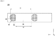
- FIG. 1 is an example of a plan view of a lighting device according to an embodiment of the invention
- FIG. 2 is a partially enlarged view of the resin layer of FIG. 1
- FIG. 3 is a view illustrating an example of a concave portion of an optical pattern portion according to an embodiment of the invention
- FIG. 4 is a view showing a modified example of the concave portion of the optical pattern portion according to an embodiment of the invention
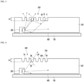
- FIG. 5 is an example of a side cross-sectional view of the lighting device of FIG. 1 in a first direction
- FIG. 6 is an enlarged view of region A1 of FIG. 5
- FIG. 7 is a first example of the optical pattern portion of the invention
- FIG. 8 is a cross-sectional side view taken along line A-A' of FIG. 7 as region A2 of FIG. 5
- FIG. 9 is an example of a cross-sectional side view taken along line B-B' of FIG. 7 .
- a lighting device 1000 may include a light emitting device 300 and a resin layer 500 sealing the light emitting device 300 and having an optical pattern portion 600.
- the lighting device 1000 may include the light emitting device 300 and the substrate 100 disposed under the resin layer 500.
- the lighting device 1000 may include a reflective member 400 disposed between the substrate 100 and the resin layer 500.
- the lighting device 1000 may emit the light emitted from the light emitting device 300 as surface light.
- the light emitting device 300 may be defined as a package having an LED chip, a light source having an LED chip, or a light source emitting visible light.
- the lighting device 1000 may be defined as a light emitting cell or a light source module.
- the lighting device 1000 may include one light emitting cell or a plurality of light emitting cells on the substrate 100.
- the substrate 100 may include a printed circuit board (PCB).
- the substrate 100 may include, for example, at least one of a resin-based printed circuit board (PCB), a PCB having a metal core, a flexible PCB, a ceramic PCB, or an FR-4 substrate.
- PCB resin-based printed circuit board
- the substrate 100 may be electrically connected to the light emitting device 300.
- the substrate 100 includes a wiring layer (not shown) thereon, and the wiring layer may be electrically connected to the light emitting device 300.
- the substrate 100 may function as a base member or a support member disposed under the light emitting device 300 and the resin layer 500.
- the upper surface of the substrate 100 may have an X-Y plane.
- the upper surface of the substrate 100 may be flat or have a curved surface.
- the thickness of the substrate 100 may be a vertical direction or a height in the Z direction.
- the X direction may be a first direction
- the Y direction may be a second direction.
- the Z direction may be a direction orthogonal to the first and second directions.
- the plurality of light emitting devices 300 may be arranged on the substrate 100 with a predetermined interval X1 in the first direction X.
- the substrate 100 may be provided in a straight or curved bar shape in a long direction.
- the substrate 100 may include a translucent material through which light is transmitted through the upper and lower surfaces.
- the light-transmitting material may include at least one of polyethylene terephthalate (PET), polystyrene (PS), and polyimide (PI).
- the substrate 100 may include an insulating layer or a reflective layer for protecting the pad and circuit pattern disposed thereon.
- the light emitting device 300 is disposed along at least a first direction X on the substrate 100, and emits light in the first direction X.
- the light emitting devices 300 may be arranged in N rows and/or M columns on the substrate 100. N and M may be 2 or more.
- the plurality of light emitting devices 300 may be arranged in a matrix having regular intervals on the substrate 100 or may be arranged in a form having irregular intervals.
- the light emitting device 300 emits light having the highest intensity in one direction.
- the light emitting device 300 may have an exit surface 381 through which light is emitted, and the exit surface 381 may be disposed, for example, in a third direction or in a vertical direction with respect to the horizontal upper surface of the substrate 100.
- the exit surface 381 may be a vertical plane, or may include a concave surface or a convex surface.
- one or a plurality of conductive frames 103 may be disposed on the lower portion of the light emitting device 300, and the conductive frame 103 is a lead frame, facing the substrate 100, and may be electrically connected to the pad of the substrate 100 by a conductive bonding member 153.
- the conductive bonding member 103 may be a solder material or a metal material.
- the light emitting device 300 may be disposed as a first light emitting device from one end of the substrate 100 and a second light emitting device in an exit direction of the first light emitting device.
- the first light emitting device and the second light emitting device irradiate light in the direction of the other end or the first direction of the substrate 100. That is, the first light emitting device irradiates light in the direction of the second light emitting device, and the second light emitting device irradiates light in the direction of the other end of the substrate 100 or the opposite side where the first light emitting device is disposed.
- the light emitting device 300 may include a device including a light emitting chip 371 in a body or a package in which the light emitting chip 371 is packaged.
- the light emitting chip 371 is an LED chip and may be molded in a body by a molding member.
- the exit surface 381 may be a surface of the molding member.
- the molding member may be made of a transparent resin material such as silicone or epoxy.
- the light emitting chip 371 may be provided as an LED chip that emits at least one of blue, red, green, ultraviolet (UV), and infrared, and the light emitting device 300 is white, blue, red, green, and infrared. At least one may emit light.
- the light emitting device 300 may be of a side view type in which a bottom portion is electrically connected to the substrate 100, but is not limited thereto.
- the light emitting device 300 may be an LED chip or a top view package.
- the exit surface 381 of the light emitting device 300 may be disposed on at least one side of the light emitting device 300 rather than the upper surface.
- the exit surface 381 may be a side adjacent to the substrate 100 or a side perpendicular to the upper surface of the substrate 100 among the side surfaces of the light emitting device 300.
- the exit surface 381 is disposed on a side surface between the bottom surface and the upper surface of the light emitting device 300 and emits light of the highest intensity in the first direction X.
- Some of the light emitted through the exit surface 381 of the light emitting device 300 travels in a direction parallel to the upper surface of the substrate 100, is reflected by the reflective member 400, or may proceed in a direction of the upper surface of the resin layer 500.
- the thickness of the light emitting device 300 may be, for example, 3 mm or less, for example, in the range of 0.8 mm to 2 mm.
- a length k1 of the light emitting device 300 in the second direction may be 1.5 times or more of a thickness of the light emitting device 300.
- the light directivity angle in ⁇ Z direction may be wider than the light directivity angle in ⁇ Y direction.
- the light directivity angle of the light emitting device 300 in the second direction Y may be 110 degrees or more, for example, 120 degrees to 160 degrees or 140 degrees to 170 degrees.
- the light directivity angle of the light emitting device 300 in the third direction Z may be 110 degrees or more, for example, 120 degrees to 140 degrees.
- the reflective member 400 may be a layer separately disposed on the substrate 100 or a layer protecting the upper portion of the substrate 100.
- the reflective member 400 may be disposed between, for example, the substrate 100 and the resin layer 500.
- the reflective member 400 may be provided in the form of a film having a metal material or a non-metal material.
- the reflective member 400 may be adhered to the upper surface of the substrate 100.
- the reflective member 400 may have an area smaller than an area of the upper surface of the substrate 100.
- the reflective member 400 may be spaced apart from the edge of the substrate 100, and a resin layer 500 may be attached to the substrate 100 in a region where the reflective member is spaced apart.
- the reflective member 400 may have a dot-shaped reflective pattern disposed on its upper surface, but is not limited thereto. As shown in FIG. 6 , the reflective member 400 may include an opening 410 in which a lower portion of the light emitting device 300 is disposed. In the opening 410 of the reflective member 400, the upper surface of the substrate 100 is exposed and a portion to which the frame of the light emitting device 300 is bonded may be disposed. The size of the opening 410 may be the same as or larger than the size of the light emitting device 300, but is not limited thereto. The reflective member 400 may be in contact with the upper surface of the substrate 100 or may be adhered between the resin layer 500 and the substrate 100.
- the reflective member 400 may be removed when a highly reflective material is coated on the upper surface of the substrate 100.
- the reflective member 400 may be formed to have a thickness smaller than that of the light emitting device 300.
- the thickness of the reflective member 400 may include a range of 0.2 mm ⁇ 0.02 mm.
- the lower portion of the light emitting device 300 may pass through the opening 410 of the reflective member 400 and an upper portion of the light emitting device 300 may protrude.
- the exit surface 381 of the light emitting device 300 may be provided in a direction perpendicular to the upper surface of the reflective member 400.
- the reflective member 400 may include a metallic material or a non-metallic material.
- the metallic material may include a metal such as aluminum, silver, or gold.
- the non-metallic material may include a plastic material or a resin material.
- the resin material may include a reflective material, for example, a metal oxide such as TiO 2 , Al 2 O 3 , SiO 2 , in silicon or epoxy.
- the reflective member 400 may be implemented as a single layer or a multilayer, and light reflection efficiency may be improved by such a layer structure.
- the reflective member 400 according to an embodiment of the invention reflects incident light, thereby increasing the amount of light so that the light is emitted uniformly. As another example, the reflective member 400 may be removed from the substrate 100.
- the resin layer 500 may be disposed on the substrate 100.
- the resin layer 500 may face or adhere to the substrate 100.
- the resin layer 500 may be disposed on the entire or partial region of the upper surface of the substrate 100.
- An area of the lower surface of the resin layer 500 may be the same as an area of the upper surface of the substrate 100, or may be equal to or greater than 80% of an area of the upper surface of the substrate 100.
- the resin layer 500 may be formed of a transparent material and may guide or diffuse light.
- the resin layer 500 includes a UV-curable resin material and may be used instead of a light guide plate, and the UV-curable resin material has an effect of convenient adjustment of refractive index and thickness.
- the resin layer 500 uses an oligomer as a main material, and mixes IBOA, monomer for dilution, and GMA, so that hardness, heat resistance, and transmittance may be adjusted, and adhesion and oxidation prevention may be suppressed.
- the resin layer 500 may contain a photo initiator and a light stabilizer to control curing and suppress discoloration. Since the resin layer 500 is provided as a layer for guiding light with a resin, it may be provided with a thinner thickness than in the case of glass and may be provided as a flexible plate.
- the resin layer 500 may emit the point light emitted from the light emitting device 300 in the form of linear light or surface light.
- a bead (not shown) may be included in the resin layer 500, and light may be diffused. Since the upper portion of the resin layer 500 is disposed on the light emitting device 300, the light emitting device 300 may be protected and loss of light emitted from the light emitting device 300 may be reduced.
- the light emitting device 300 may be buried under the resin layer 500.
- the resin layer 500 may be in contact with the surface of the light emitting device 300 and may be in contact with the exit surface 381 of the light emitting device 300.
- a portion of the resin layer 500 may be disposed in the opening 410 of the reflective member 400.
- a portion of the resin layer 500 may be in contact with the upper surface of the substrate 100 through the opening 410 of the reflective member 400. Accordingly, a portion of the resin layer 500 is in contact with the substrate 100, thereby fixing the reflective member 400 between the resin layer 500 and the substrate 100.
- the thickness of the resin layer 500 may be 5 mm or less, for example, 2 mm to 5 mm. When the thickness of the resin layer 500 is thicker than the above range, luminous intensity or light blocking characteristics may be reduced, and it may be difficult to provide a flexible module due to an increase in the module thickness. When the thickness of the resin layer 500 is smaller than the above range, it is difficult to provide surface light having a uniform luminous intensity.
- the length of the resin layer 500 in the first direction X may be disposed along the first direction of the substrate 100, and the length of the second direction Y may be disposed along the second direction of the substrate 100.
- the resin layer 500 may be disposed in a range of 80% or more, for example, 80% to 100% of the length of the substrate 100 in the first and second directions.
- Each side surface of the resin layer 500 may be disposed on the same plane or adjacent to each side surface of the substrate 100.
- the resin layer 500 may be provided in a size to cover the plurality of light emitting devices 300 or may be connected to each other.
- the resin layer 500 may be divided into a size to cover each light emitting device 300, and may be divided into light emitting cells having each light emitting device 300 and each resin layer 500.
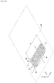
- the resin layer 500 may include an optical pattern portion 600.
- the optical pattern portion 600 reflects or refracts incident light to suppress hot spots.
- the optical pattern portion 600 may be formed in a concave pattern on the upper surface of the resin layer 500.
- the concave pattern may include concave portions 60 arranged to have a predetermined depth on the upper surface of the resin layer 500.
- the optical pattern portions 600 may be disposed on each of the upper portions of the light emitting devices 300, and may include concave portions 60 formed from the upper surface of the resin layer 500 toward the substrate 100.
- the convex portions 70 may be disposed between the concave portions 60.
- Each of the plurality of optical pattern portions 600 may be spaced apart from each other along a direction (e.g., X) in which the light emitting devices 300 are disposed. For example, an interval X2 between the optical pattern portions 600 may be smaller than the interval X1 between the light emitting devices 300.
- Each of the optical pattern portions 600 may be spaced apart from an outer side surface or an edge of the resin layer 500.
- the first portion of the optical pattern portion 600 may be a region overlapping the light emitting device 300 in a vertical direction or a third direction Z.
- the second portion of the optical pattern portion 600 may be a peripheral region of the first portion, and may be an upper region from which light is emitted based on the first portion.
- the plurality of optical pattern portions 600 may refract or reflect light incident on top of each of the plurality of light emitting devices 300 to suppress hot spots on each of the upper portions of the light emitting devices 300.
- each of the optical pattern portions 600 may have a maximum length b2 in the second direction Y greater than a maximum length b1 in the first direction X.
- Each of the optical pattern portions 600 may be disposed in a region having a radius of 10 mm or less in a long axis direction (e.g., a second direction) from the center of each of the optical pattern portions 600 and a radius of 6 mm or less in the minor axis direction.
- the maximum length b1 of the optical pattern portion 600 in the first direction X may be 8 mm or more, for example, in the range of 8 mm to 12 mm.
- the maximum length b2 of the optical pattern portion 600 in the second direction Y may be 10 mm or more, for example, in the range of 10 mm to 20 mm or in the range of 12 mm to 20 mm.
- Each of the optical pattern portions 600 may have a size corresponding to a characteristic of the light directivity angle of the light emitting device 300, that is, the light directivity angle in the second direction Y with respect to the optical axis is larger than the directivity angle in the third direction Z. Accordingly, the optical pattern portion 600 may effectively refract or reflect light traveling in the third direction Z from the front of the light emitting device 300 with respect to the optical axis, and may effectively refract or reflect light proceeding in the second direction Y. Accordingly, the optical pattern portion 600 may improve the light diffusion efficiency by lowering the straightness of the incident light.
- the width k2 of the first portion overlapping the upper portion of the light emitting device 300 of the optical pattern portion 600 may be greater than the length k1 of the light emitting device 300. Accordingly, the light progressing upwards of the light emitting device 300 may be effectively refracted and diffused in other directions.
- the light emitting devices 300 when the light emitting devices 300 are arranged in the first direction X, it may be defined as a first light emitting device and a second light emitting device.
- the optical pattern portions 600 are arranged in the first direction X, it may be defined as a first optical pattern portion and a second optical pattern portion.
- the first light emitting device emits light toward the front or the rear of the second light emitting device
- the second light emitting device emits light toward the front.
- the first optical pattern portion covers the upper surface and the front upper portion of the first light emitting device on the upper surface of the resin layer 500
- the second optical pattern portion covers the upper surface and the front upper portion of the second light emitting device on the upper surface of the resin layer 500.
- the first and second optical pattern portions may refract or reflect light incident from each of the first and second light emitting devices to diffuse the light.
- the optical pattern portion 600 having an uneven pattern is disposed on the surface of the resin layer 500, a structure including a layer for separately forming a light blocking member on the resin layer 500 or an adhesive layer for bonding a layer having a light blocking member to the resin layer may be removed.
- a diffusion plate may be further provided on the resin layer 500, or an inner or outer lens may be further provided on the resin layer 500. Accordingly, it is possible to provide a thin thickness of the lighting device 1000, and the refracted light travels in the direction of the light, thereby improving the distribution of the light.
- the optical pattern portion 600 includes a plurality of concave portions 60, and the top view shape of the concave portion 60 may be a polygonal shape (e.g., a triangle, a square or a pentagon), a circular shape or an elliptical shape.
- the upper surface area of each of the concave portions 60 may be provided with the same size or different sizes.
- the upper surface area of each of the concave portions 60 may be disposed to have the same size according to regions, and may be provided to have different sizes in different regions.
- the concave portions 60 may be spaced apart from each other by a predetermined interval, and the interval may be smaller than lengths of the concave portions 60 in the first and second directions X and Y.
- Interval between the concave portions 60 may be equal to each other.
- the interval between the concave portions 60 may include a region having a constant interval and a region having a smaller or larger interval than the constant interval.
- the concave portions 60 may have the same or different intervals in the first direction X and in the second direction Y.
- concave portions 60 and convex portions 70 may be alternately arranged in the first direction X.
- the concave portions 60 and the convex portions 70 may be alternately arranged in the second direction Y.
- a side cross-section of each of the concave portions 60 may have a polygonal shape.
- the width of the concave portions 60 in the first direction X and/or the second direction Y may be smaller than the depth h1.
- the concave portions 60 may have a columnar shape having a deep depth h1.
- the concave portion 60 may have an upper width and the same lower width.
- a bottom 6 of the concave portion 60 may include a flat surface.
- the upper surface 7 of the convex portion 70 between the concave portions 60 may have a constant width or may have different widths according to regions.
- the convex portions 70 may be connected to each other, and the concave portions 60 may be provided in a shape recessed in the lower surface direction in the inner region of the convex portions 70.
- the concave portion 60 may reflect or refract incident light, and may diffuse the incident light.
- the convex portion 70 may reflect or refract incident light, or guide it upward to diffuse it.
- a side cross-section of each of the concave portions 60A of the optical pattern portion 600 may have a columnar shape.
- a lower portion of the concave portions 60A may have a hemispherical shape, and the bottom 6A may include a concave curved surface.
- the width of the concave portions 60A in the first direction and/or the second direction may be smaller than the depth h1.
- the concave portion 60A may have an upper width greater than a lower minimum width.
- the upper surface 7A of the convex portion 70A between the concave portions 60A may have a constant width or may have different widths according to regions.
- the convex portions 70A may be connected to each other, and the concave portions 60A may be provided in a shape recessed in the lower surface direction within the region of the convex portion 70A.
- the curvature of the curved surface of the concave portion 60A may be 0.08 or more, for example, in the range of 0.08 to 0.12. It is possible to improve the emitting efficiency of light incident by the curved surface having such a curvature.
- the curvature of the concave portion 60A may be a curvature between the bottom 6A and the side surface, or a curvature of a corner portion between the side surfaces in the concave portion 60A.
- the width of the concave portion 60A may be 0.25 mm or more, for example, in the range of 0.25 mm to 0.45 mm.
- the angle at which the light incident on the concave curved surface of the concave portion 60A is refracted and the angle at which the light is emitted are the same as in Equations 1 to 3 for light extraction.
- 90 ⁇ ⁇ 4 asin 1.47 sin 90 ⁇ ⁇ 3 47.1 ° ⁇ 90 ⁇ ⁇ 3 ⁇ 90 ° 0 ° ⁇ 90 ⁇ ⁇ 3 ⁇ 47.1 °
- the angle ⁇ 3 is an angle of light incident with respect to a tangent passing through the curved surface of the concave portion 60A
- the angle ⁇ 4 is an angle of light refracted with respect to a tangent passing through the curved surface of the concave portion 60A
- the angle ⁇ 5 is the angle between the light transmitted through the concave portion 60A and the horizontal upper surface of the resin layer 500.
- the angle ⁇ 5 may be in the range of 35 ⁇ 15 degrees.
- the condition of Equation 2 is an angle at which light incident on the concave portion 60A is totally reflected, and the transmittance of the light may be lowered.
- the bottom curvature of the concave portion 60A may be designed in consideration of the critical angle of the material of the resin layer 500.
- the condition of Equation 3 is an angle at which light incident on the concave portion 60A is transmitted, and the light may be refracted and emitted to the outside.
- the angle ⁇ 5 between the refracted and transmitted light and the horizontal upper surface of the resin layer 500 the efficiency of emitting light emitted from the light emitting device 300 in front direction may be increased, so that the light distribution of the lighting device may have directionality. That is, when the lighting device is disposed on the side of the vehicle lamp, the light emitted from the light emitting device 300 may be emitted at the angle ⁇ 5. Accordingly, the lighting device disposed on the rear side of the vehicle lamp may provide the directionality of the light distribution that proceeds in the rear direction.
- the depth h1 of the concave portions 60 and 60A of the optical pattern portion 600 may be 0.25 mm or more, for example, in the range of 0.25 mm to 0.8 mm.
- the depth h1 of the concave portions 60 and 60A of the optical pattern portion 600 may be constant or may have different depths depending on the regions. For example, when the concave portions 60 and 60A have different depths h1 depending on the regions, the first region adjacent to the light emitting device 300 is deep and the second region(s) farther from the light emitting device 300 may have a smaller depth than a depth of the first region.
- the concave portions 60 and 60A may be formed by etching or may be formed by a molding process of the resin layer 500.
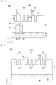
- FIGs. 7 to 9 are views showing the optical pattern portion according to the first example of the invention.
- the maximum length b2 in the second direction Y may be greater than the maximum length b1 in the first direction X, for example, the maximum length b2 in the second direction Y may be 120% or more, for example, 120% to 180% of the maximum length b1 in the first direction X.
- the area of the region connecting the outermost patterns of the optical pattern portion 600 may be 6 times or more, for example, 6 times to 18 times the upper surface area of the light emitting device 300. Accordingly, the optical pattern portion 600 may cover the upper portion and the front region of the light emitting device 300 to reflect or refract the incident light.
- widths w1, w2, w3, and w4 of the plurality of pattern portions 610, 620, 630, and 640 arranged in the first direction X may be different from each other.
- the plurality of pattern portions 610, 620, 630, and 640 may extend in the second direction Y.
- the plurality of pattern portions 610, 620, 630, and 640 may be disposed at the same depth h1, and the pitches P1, P2, P3, and P4 between the concave portions 61, 62, 63, and 64 adjacent in the first and second directions X and Y may be the same or may become wider as a distance from the exit surface 381 of the light emitting device 300 increases.
- Each of the plurality of pattern portions 610, 620, 630 and 640 includes concave portions 61, 62, 63, 64 and convex portions 71, 72, 73, 74, and the concave portions 61, 62, 63, 64 and the convex portions 71, 72, 73, and 74 may be alternately disposed.
- Intermediate convex portions 77, 78, and 79 between the plurality of pattern portions 610, 620, 630, and 640 are larger than at least two of the widths w1, w2, w3 and w4 of the adjacent concave portions 61, 62, 63 and 64, and may be equal to or greater than the width of at least one of the widths of the adjacent convex portions 71, 72, 73, and 74.
- the optical pattern portion 600 may disposed in the order of a first pattern portion 610, a second pattern portion 620, a third pattern portion 630, and a fourth pattern portion 640 in a first direction X from the center of the position where the light emitting device 300 is placed.
- the optical pattern portion 600 may be disposed in the order of a first pattern portion 610, a second pattern portion 620, a third pattern portion 630 and a fourth pattern portion 640 on both sides in the second direction Y from the position where the light emitting device 300 is placed or the center of the optical pattern portion 600.
- Intermediate convex portions 77, 78, and 79 may be disposed between the first to fourth pattern portions 610, 620, 630 and 640, respectively.
- first to fourth pattern portions 610, 620, 630 and 640 concave portions 61, 62, 63, 64 and convex portions 71, 72, 73 and 74 may be alternately disposed.
- the first pattern portion 610 includes a plurality of first concave portions 61 and a plurality of first convex portions 71, and the width w1 of the first concave portion 61 may be greater than a width of the first convex portion 71 disposed between the first concave portions 61.
- the second pattern portion 620 includes a plurality of second concave portions 62 and a plurality of second convex portions 72, and the width w2 of the second concave portion 62 may be greater than a width of the second convex portion 72 disposed between the second concave portions 62.
- the third pattern portion 630 includes a plurality of third concave portions 63 and a plurality of fourth convex portions 73, and the width w3 of the third concave portion 63 may be smaller than a width of the third convex portion 73 disposed between the third concave portions 63.
- the fourth pattern portion 640 includes a plurality of fourth concave portions 64 and at least one fourth convex portion 74, and the width of the fourth concave portion 64 may be smaller than a width of the fourth convex portion 74 disposed between the fourth concave portion 64.
- Widths w1, w2, w3 and w4 of the first to fourth concave portions 61, 62, 63, and 64 may gradually decrease in the first direction X based on a position overlapping the center of the light emitting device 300. Widths w1, w2, w3 and w4 of the first to fourth concave portions 61, 62, 63, and 64 may gradually decrease from a position overlapping with the center of the light emitting device 300 or from the center of the optical pattern portion 600 toward both sides of the second direction Y.
- the width of each of the first to fourth concave portions 61, 62, 63, and 64 may satisfy the following condition: w1 > w2 > w3 > w4.
- the width w1 is 0.4 mm or more, for example, in the range of 0.4 mm to 0.6 mm, the width w2 is less than 0.4 mm, for example, in the range of 0.32 mm to 0.39 mm, and the width w3 is 0.3 mm or less, for example, in the range of 0.29 mm to 0.38 mm, and the width w4 may be 0.2 mm or more, for example, in the range of 0.2 mm to 0.28 mm.
- the width w1 of the first concave portion 61 may be at least twice the width w4 of the fourth concave portion 64.
- the widths d1, d2, and d3 of the intermediate convex portions 77, 78, and 79 may satisfy the following condition: d1 ⁇ d2 ⁇ d3, and may be a minimum of 0.01 mm or more and a maximum of 0.5 mm or less. That is, the maximum width d3 may be in the range of 0.4 mm to 0.5 mm, and the minimum width d1 may be in the range of 0.01 to 0.2 mm. This minimum width d1 may be a range in which concave portions between the convex portions 77 may be etched or formed.
- the depth h1 of the first to fourth concave portions 61, 62, 63, and 64 may be 0.25 mm or more, for example, in the range of 0.25 mm to 0.35 mm.
- the area of the upper surface of the optical pattern portion 600 may be in the range of 40% ⁇ 5% compared to an area of the upper surface of the optical pattern portion 600
- an area of the upper surface of the second pattern portion 620 may be in the range of 25% ⁇ 4% compared to the area of the upper surface of the optical pattern portion 600
- an area of the upper surface of the third pattern portion 630 may be in the range of 20% ⁇ 3% compared to the area of the optical pattern portion 600
- an area of the upper surface of the fourth pattern portion 640 may be in the range of 15% ⁇ 3% compared to the area of the upper surface of the optical pattern portion 600.
- the depth h1 of the optical pattern portion 600 having the plurality of pattern portions 610, 620, 630, and 640 is the same, and the pattern portions having the concave portions 61, 62, 63, and 64 farther away from an overlapping position with the center of the light emitting device 300 may be provided with a gradually smaller width. Accordingly, an area of the concave portion of the first pattern portion 610 is the largest in the region adjacent to the light emitting device 300, and an area of the concave portion may be reduced as the region is farther from the light emitting device 300, so that patterns capable of diffusing light in proportion to the light intensity may be disposed.
- FIGs. 10 to 12 are views illustrating an optical pattern portion according to a second example.
- the maximum length b4 in the second direction Y may be equal to or greater than the maximum length b3 in the first direction X, for example, the maximum length b4 in the second direction Y may be 200% or more, for example, in the range of 200% to 330% of the maximum length b3 in the first direction X.
- the maximum length b3 in the first direction X may be equal to or greater than the length k1 (in FIG. 2 ) of the light emitting device 300.
- the maximum length b3 in the first direction X may be 3.5 mm or less, for example, in the range of 2.5 mm to 3.5 mm
- the maximum length b4 in the second direction Y may be 7 mm or more, for example, in the range from 7 mm to 9 mm.
- the area of the region connecting the outermost patterns of the optical pattern portion 600 may be one or more times, for example, one to three times the area of the upper surface of the light emitting device 300. Accordingly, the optical pattern portion 600A may cover the upper portion and the front region of the light emitting device 300 to reflect or refract the incident light.
- widths w1 and w2 of the plurality of pattern portions 610 and 620 arranged in the first direction X may be different from each other.
- the plurality of pattern portions 610 and 620 may extend in the second direction Y.
- the plurality of pattern portions 610 and 620 may be disposed to have the same depth h2 as each other, and the pitches p1 and p2 between the concave portions 62 adjacent in the first and second directions X and Y may be the same or may be gradually increased.
- Each of the plurality of pattern portions 610 and 620 includes concave portions 61 and 62 and convex portions 71 and 72, and the concave portions 61 and 62 and the convex portions 71 and 72 may be alternately disposed.
- the intermediate convex portion 77 between the plurality of patterns may be greater than the widths w1 and w2 of the adjacent concave portions 61 and 62, and may be equal to or greater than the width of at least one of the adjacent convex portions 71.
- the optical pattern portion 600A has a first pattern portion 610 and a second pattern portion 620 disposed in a first direction, and an intermediate convex portion 77 may be disposed between each of the first pattern portions 610 and each of the second pattern portions 620.
- the concave portions 61 and 62 and the convex portions 71 and 72 may be alternately disposed in each of the first and second pattern portions 610 and 620.
- the first pattern portion 610 includes a plurality of first concave portions 61 and a plurality of first convex portions 71, and the width w1 of the first concave portion 61 may be greater than a width of the first convex portions 71 disposed between the first concave portions 61.
- the second pattern portion 620 includes a plurality of second concave portions 62 and a plurality of second convex portions 72, and the width w2 of the second concave portion 62 may be greater than a width of the second convex portion 72 disposed between the second concave portions 62.
- Widths w1 and w2 of the first concave portion 61 and the second concave portion 62 in the first direction X may be gradually smaller based on a position overlapping the center of the light emitting device 300.
- the widths (w1>w2) of the first concave portion 61 and the second concave portion 62 arranged toward both sides in the second direction Y may be gradually decreased from a position overlapping the center of the light emitting device 300 or from the center of the optical pattern portion 600A.
- the width of each of the first and second concave portions 61 and 62 may satisfy the following condition: w1>w2.
- the width w1 may be 0.4 mm or more, for example, in the range of 0.4 mm to 0.6 mm, and the width w2 may be less than 0.4 mm, for example, in the range of 0.25 mm to 0.39 mm.
- the width w1 of the first concave portion 61 may be less than or equal to twice the width w2 of the second concave portion 62.
- the width d1 of the intermediate convex portion 77 may be in the range of 0.01 mm to 0.5 mm, and may be larger than the widths of the first and second convex portions 71 and 72.
- the depth h2 of the first and second concave portions 61 and 62 may be 0.4 mm or more, for example, in the range of 0.4 mm to 0.5 mm.
- the upper surface area of the first pattern portion 610 may be in the range of 80% ⁇ 5% compared to an area of the upper surface of the optical pattern portion 600A
- an area of the upper surface of the second pattern portion 620 may be in the range of 20% ⁇ 4% compared to an area of the upper surface of the optical pattern portion 600A.
- the depth h2 of the optical pattern portion 600A having the plurality of pattern portions 610 and 620 is deeper than the depth h1 of the first example and is equal to each other, and may be gradually reduced as the distance from the overlapping position with the center of the light emitting device 300 increases. Accordingly, an area of the first concave portion 61 of the pattern portions 610 and 620 is the largest in a region adjacent to the light emitting device 300, and the area of the second concave portion 62 may be reduced as the region is farther away the light emitting device 300, so that patterns capable of diffusing light in proportion to the light intensity may be disposed.
- FIGs. 13 to 15 are views illustrating an optical pattern portion according to a third example.
- the maximum length b6 in the second direction Y may be greater than the maximum length b5 in the first direction X, for example, the maximum length b6 in the second direction Y may be 100% or more than the maximum length b5 in the first direction X, for example, in the range of 100% to 150%.
- the maximum length b5 in the first direction X may be 80% or more, for example, 80% to 110% of the length k1 (in FIG. 2 ) of the light emitting device 300.
- the maximum length b5 in the first direction X may be in the range of 2.5 mm or less, for example, 1.8 mm to 2.5 mm
- the maximum length b6 in the second direction Y is 7 mm or more, for example, in the range from 7 mm to 9 mm.
- the area of the region connecting the outermost patterns of the optical pattern portion 600B may be 0.5 times or more, for example, in the range of 0.5 times to 1.5 times an area of the upper surface of the light emitting device 300. Accordingly, the optical pattern portion 600B may cover an upper portion of the light emitting device 300 and a front region thereof to reflect or refract incident light.
- widths w1 and w2 of the plurality of pattern portions 610 and 620 arranged in the first direction X may be different from each other.
- the plurality of pattern portions 610 and 620 may extend in the second direction Y.
- the plurality of pattern portions 610 and 620 may be disposed to have the same depth h3 as each other, and the pitch p1 between the concave portions 62 adjacent in the first and second directions X and Y may be the same.
- Each of the plurality of pattern portions 610 and 620 includes concave portions 61 and 62 and convex portions 71 and 72, and the concave portions 61 and 62 and the convex portions 71 and 72 may be alternately disposed.
- the intermediate convex portion 77 between the plurality of pattern portions 610 and 620 may be smaller than the width w1 of at least one of the adjacent concave portions 61 and 62 and greater than the width of the adjacent convex portions 71 and 72.
- the optical pattern portion 600B has a first pattern portion 610 and a second pattern portion 620 disposed in a first direction, and an intermediate convex portion 77 may be disposed between each of the first and second pattern portions 610 and 620.
- the concave portions 61 and 62 and convex portions 71 and 72 may be alternately disposed in the first and second directions.
- the first pattern portion 610 includes a plurality of first concave portions 61 and a plurality of first convex portions 71, and the width w1 of the first concave portion 61 may be greater than a width of the first convex portion 71 disposed between the first concave portions 61.
- the second pattern portion 620 includes a plurality of second concave portions 62 and a plurality of second convex portions 72, and the width w2 of the second concave portion 62 may be equal to or different from a width of the second convex portion 72 disposed between the second concave portions 62.
- Widths w1 and w2 of the first concave portion 61 and the second concave portion 62 in the first direction X may be gradually smaller based on a position overlapping the center of the light emitting device 300.
- the width (w 1 >w2) of first concave portion 61 and the second concave portion 62 arranged toward both sides in the second direction Y from a position overlapping the center of the light emitting device 300 or from the center of the optical pattern portion 600B may gradually decrease.
- the width of each of the first and second concave portions 61 and 62 may satisfy the following conduction: w1>w2.
- the width w1 may be 0.4 mm or more, for example, in the range of 0.4 mm to 0.6 mm, and the width w2 may be less than 0.4 mm, for example, in the range of 0.25 mm to 0.39 mm.
- the width w1 of the first concave portion 61 may be less than or equal to twice the width w2 of the second concave portion 62.
- the width d1 of the intermediate convex portion 77 may be in the range of 0.01 mm to 0.5 mm, and may be greater than the widths of the first and second convex portions 71 and 72.
- the depth h3 of the first and second concave portions 61 and 62 may be 0.55 mm or more, for example, in the range of 0.55 mm to 0.65 mm.
- an area of the upper surface of the optical pattern portion 600B is 100%, an area of the upper surface of the first pattern portion 610 may be in the range of 85% ⁇ 5% compared to the area of the upper surface of the optical pattern portion 600B, and an area of the upper surface of the second pattern portion 620 may be in the range of 15% ⁇ 4% compared to the area of the upper surface of the optical pattern portion 600B.
- the depth h3 of the optical pattern portion 600B having the plurality of pattern portions 610 and 620 is deeper than the depth h2 of the second example and is equal to each other, and may be gradually reduced as the distance from overlapping position with the center of the light emitting device 300 increases. Accordingly, an area of the first concave portion 61 of the pattern portions 610 and 620 is the largest in the region adjacent to the light emitting device 300, and the area of the second concave portion 62 may be reduced as the region is farther away the light emitting device 300, so that patterns capable of diffusing light in proportion to the light intensity may be disposed.
- FIGs. 16 and 17 are views illustrating an optical pattern portion according to a fourth example.
- the maximum length b2 in the second direction Y may be greater than the maximum length b1 in the first direction X, for example, the maximum length b2 in the second direction Y may be 120% or more, for example, 120% to 180% of the maximum length b1 in the first direction X.
- An area of the region connecting the outermost patterns of the optical pattern portion 600C may be 6 times or more, for example, 6 to 18 times an area of the upper surface of the light emitting device 300. Accordingly, the optical pattern portion 600C may cover the upper portion and the front region of the light emitting device 300 to reflect or refract the incident light.
- widths w1, w2, w3, and w4 of the plurality of pattern portions 610, 620, 630, and 640 arranged in the first direction X may be different from each other.
- the plurality of pattern portions 610, 620, 630, and 640 may extend in the second direction.
- the plurality of pattern portions 610, 620, 630, and 640 may have a different depths h1, h2, h3 and h4, and the pitches P1, P2, P3, and P4 between the concave portions 62 adjacent in the first and second directions may be different from each other.
- Each of the plurality of pattern portions 610, 620, 630 and 640 includes concave portions 61, 62, 63, 64 and convex portions 71, 72, 73, 74, and the concave portions 61, 62, 63, 64 and the convex portions 71, 72, 73, and 74 may be alternately disposed.
- the intermediate convex portions 77, 78, and 79 between the plurality of pattern portions 610, 620, 630, and 640 may have a smaller widths d1, d2, and d3 than the widths w1 and w2 of the adjacent first and second concave portions 61 and 62, and may have widths d1, d2, and d3 greater than widths w3 and w4 of the adjacent third and fourth concave portions 63 and 64.
- the width d1, d2, and d3 of the intermediate convex portions 77, 78, 79 is the smallest width d1 of the first intermediate convex portion 77 between the first and second pattern portions 610 and 620, and the width d3 of the third intermediate convex portion 79 between the third and fourth pattern portions 630 and 640 may be the largest.
- the width d1, d2, and d3 of the intermediate convex portions 77, 78 and 79 may be set.
- the optical pattern portion 600C may disposed in the order of a first pattern portion 610, a second pattern portion 620, a third pattern portion 630, and a fourth pattern portion 640 in a first direction X and the first pattern portion 610, the second pattern portion 620, the third pattern portion 630, and may disposed in the order of a first pattern portion 610, a second pattern portion 620, a third pattern portion 630 and a fourth pattern portion 640 on both sides in the second direction Y.
- Intermediate convex portions 77, 78, and 79 may be disposed between the first to fourth pattern portions 610, 620, 630 and 640, respectively.
- concave portions 61, 62, 63, 64 and convex portions 71, 72, 73, and 74 may be alternately disposed in first and second directions X and Y.
- the first pattern portion 610 includes a plurality of first concave portions 61 and a plurality of first convex portions 71, and the width w1 of the first concave portion 61 may be greater than a width the first convex portion 71 disposed between the first concave portions 61.
- the second pattern portion 620 includes a plurality of second concave portions 62 and a plurality of second convex portions 72, and the width w2 of the second concave portion 62 may be greater than a width of the second convex portion 72 disposed between the second concave portion 62.
- the third pattern portion 630 includes a plurality of third concave portions 63 and a plurality of third convex portions 73, and the width w3 of the third concave portion 63 may be smaller than a width of the third convex portion 73 disposed between the third concave portions 63.
- the fourth pattern portion 640 includes a plurality of fourth concave portions 64 and at least one fourth convex portion 74, and the width w4 of the fourth concave portion 64 may be smaller than a width of the fourth convex portion 74 disposed between the fourth concave portions 64.
- Widths w1, w2, w3 and w4 of the first to fourth concave portions 61, 62, 63, and 64 may gradually decrease as the distance from the position overlapping the center of the light emitting device 300 in the first direction X increases. Widths w1, w2, w3 and w4 of the first to fourth concave portions 61, 62, 63, and 64 may gradually decrease from a position overlapping with the center of the light emitting device 300 or from the center of the optical pattern portion 600 toward both sides of the second direction Y. For example, a width of each of the first to fourth concave portions 61, 62, 63, and 64 may satisfy the following condition: w1 > w2 > w3 > w4.
- the width w1 is 0.4 mm or more, for example, in the range of 0.4 mm to 0.6 mm, the width w2 is less than 0.4 mm, for example, in the range of 0.32 mm to 0.39 mm, and the width w3 is 0.3 mm or less, for example, in the range of 0.29 mm to 0.38 mm, and the width w4 may be 0.2 mm or more, for example, in the range of 0.2 mm to 0.28 mm.
- the width w1 of the first concave portion may be at least twice the width w4 of the fourth concave portion.
- the widths d1, d2, and d3 of the intermediate convex portions 77, 78, and 79 may satisfy the following condition: d1 ⁇ d2 ⁇ d3, and may be a minimum of 0.01 mm or more and a maximum of 0.5 mm or less. That is, the maximum width d3 may be in the range of 0.4 mm to 0.5 mm, and the minimum width d1 may be in the range of 0.01 to 0.2 mm. This minimum width d1 may be a range in which concave portions between the convex portions 77 may be etched or formed.
- the depths h1, h2, and h3 of the first to fourth concave portions 61, 62, 63, and 64 are equal to the depths h1 of the third or fourth concave portions 63 and 64, or the third concave portion 63 may be deeper than the four concave portion 64.
- the depth h1 of the third or fourth concave portions 63 and 64 may be smaller than the depths h3 and h2 of the first and second concave portions 61 and 62.
- a depth h3 of the first concave portion 61 may be greater than a depth h2 of the second concave portion 62.
- Depths h3, h2 and h1 of the first to fourth concave portions 61, 62, 63, and 64 as the distance in the first direction X increases with respect to the position overlapping the center of the light emitting device 300 may be gradually reduced.
- Depths h3, h2 and h1 of the first to fourth concave portions 61, 62, 63, and 64 may be gradually reduced as the distance from a position overlapping position with the center of the light emitting device 300 or from the center of the optical pattern portion 600C increases toward both sides in the second direction Y.
- the depth h1 of the third and fourth concave portions 63 and 64 may be 0.25 mm or more, for example, in the range of 0.25 mm to 0.35 mm.
- the depth h2 of the second concave portion 62 may be 0.4 mm or more, for example, in the range of 0.4 mm to 0.5 mm.
- the depth h3 of the first concave portion 61 may be 0.55 mm or more, for example, in the range of 0.55 mm to 0.65 mm.
- an area of the upper surface of the first pattern portion 610 may be in the range of 40% ⁇ 5% compared to an area of the upper surface of the optical pattern portion 600C
- an area of the upper surface of the second pattern portion 620 may be in the range of 25% ⁇ 4% compared to the area of the upper surface of the optical pattern portion 600C
- an area of the upper surface of the third pattern portion 630 may be in the range of 20% ⁇ 3% compared to the area of the upper surface of the third optical portion 600C
- an area of the upper surface of the fourth pattern portion 640 may be in the range of 15% ⁇ 3% compared to the area of the upper surface of the optical pattern portion 600C.
- the depths h1, h2, and h3 of the optical pattern portion 600C having the plurality of pattern portions 610, 620, 630, and 640 may provide the deepest at a position overlapping the center of the light emitting device 300 and the depth gradually decreases as the distance from the center of the light emitting device 300 increases, and may be provided with a gradually smaller width as the distance from the overlapping position with the center of the light emitting device 300 increases.
- the area and depth of the concave portion 61 of the first pattern portion 610 is the largest, and the area and depth may be reduced as the concave portion is farther from the light emitting device 300, so that patterns capable of diffusing light in proportion to the light intensity may be disposed.
- Table 1 shows examples in which a structure (comparative example) without an optical pattern and the luminance of a module having an optical pattern portion as in Examples 1 to 3 of the invention were compared and tested.
- Luminance (Nit) Comparative example Example 1
- Example 2 Example 3 Minimum 4330 4792 4898 4949 Maximum 77495 87234 90144 101909 Intermediate 15141 20458 20599 20564
- the maximum value of the luminance of the comparative example without the optical pattern is the lowest and the intermediate value of the luminance is also the lowest, the incident light is totally reflected and proceeds into the resin layer. Since the maximum and intermediate values of the luminance of the first example are increased, it may be seen that the amount of total reflection by the optical pattern portion is reduced, and the light extraction efficiency is improved. In the luminance of the second example, the maximum value may be increased, and the amount of light emitted from the entire region may be increased. In the luminance of the third example, the maximum value may be increased, and the amount of light emitted from the entire region may be increased. Accordingly, even if a separate light blocking member is not disposed on the resin layer having the optical pattern portion, the uniformity of light may be improved and the amount of transmitted light refracted on the optical pattern portion may be increased.
- FIG. 18(a)(b)(c) shows the directivity distribution of light in Examples 1 to 3, and (d) is a view showing the directivity distribution of light in comparative example without an optical pattern.
- the flux distribution is measured at an angle of 35 degrees with respect to the horizontal direction passing through the center of the light emitting device.
- FIG. 18 (a)(b)(c) is detected at 24 cd or more, and (d) is about 20.5 cd, which is lower than the examples of the invention.
- FIG. 19 is a plan view of a vehicle to which the lighting device according to an embodiment of the invention is applied
- FIG. 20 is a view showing an example of a tail lamp of the vehicle of FIG. 19 .
- a front lamp 850 in the moving object or vehicle 900 may include one or more lighting modules, and control the driving timing of these lighting modules individually to function as a typical headlamp as well as, when the driver opens the vehicle door, additional functions such as a welcome light or a celebration effect can be provided.
- the lamp may be applied to a daytime running lamp, a high beam, a low beam, a fog lamp or a turn signal lamp.
- the tail lamp 800 may be arranged with a plurality of lamp units 810, 812, 814, and 816 supported by the housing 801.
- the lamp units 810, 812, 814, and 816 may include a first lamp unit 810 disposed outside, a second lamp unit 814 disposed around the inner circumference of the first lamp unit 810, and third and fourth lamp units 814 and 816 respectively disposed on the inside the second lamp unit 814.
- the first to fourth lamp units 810, 812, 814, and 816 may selectively apply the lighting device disclosed in the embodiment, and a red lens cover or a white lens cover for the lighting characteristics of the lamp units 810, 812, 814, and 816 on the outside of the lighting device may be placed.
- the lighting device disclosed in the embodiment applied to the lamp units 810, 812, 814, and 816 may emit surface light in a uniform distribution.
- the first and second lamp units 810 and 812 may be provided in at least one of a curved shape, a straight shape, an angled shape, an inclined shape, and a flat shape, or a mixed structure thereof.
- One or a plurality of the first and second lamp units 810 and 812 may be disposed in each tail lamp.
- the first lamp unit 810 may be provided as a tail lamp
- the second lamp unit 812 may be provided as a brake lamp
- the third lamp unit 814 may be provided as a reverse lamp
- the fourth lamp unit 816 may be provided as a turn signal lamp.
- the structure and position of these lighting lamps can be changed.
- Such a lighting lamp may provide a higher luminous intensity in a rear direction than in a lateral direction, and thus may comply with light distribution regulations such as a stop lamp or a tail lamp.
Landscapes
- Engineering & Computer Science (AREA)
- General Engineering & Computer Science (AREA)
- Physics & Mathematics (AREA)
- Optics & Photonics (AREA)
- General Physics & Mathematics (AREA)
- Microelectronics & Electronic Packaging (AREA)
- Planar Illumination Modules (AREA)
- Non-Portable Lighting Devices Or Systems Thereof (AREA)
Priority Applications (1)
| Application Number | Priority Date | Filing Date | Title |
|---|---|---|---|
| EP26164456.1A EP4733816A2 (fr) | 2020-05-20 | 2021-05-13 | Dispositif d'éclairage |
Applications Claiming Priority (2)
| Application Number | Priority Date | Filing Date | Title |
|---|---|---|---|
| KR1020200060350A KR20210143501A (ko) | 2020-05-20 | 2020-05-20 | 조명모듈, 조명장치 및 후미등 |
| PCT/KR2021/006026 WO2021235774A1 (fr) | 2020-05-20 | 2021-05-13 | Module d'éclairage, dispositif d'éclairage et feu arrière |
Related Child Applications (2)
| Application Number | Title | Priority Date | Filing Date |
|---|---|---|---|
| EP26164456.1A Division-Into EP4733816A2 (fr) | 2020-05-20 | 2021-05-13 | Dispositif d'éclairage |
| EP26164456.1A Division EP4733816A2 (fr) | 2020-05-20 | 2021-05-13 | Dispositif d'éclairage |
Publications (3)
| Publication Number | Publication Date |
|---|---|
| EP4155603A1 true EP4155603A1 (fr) | 2023-03-29 |
| EP4155603A4 EP4155603A4 (fr) | 2024-06-05 |
| EP4155603B1 EP4155603B1 (fr) | 2026-04-15 |
Family
ID=78697957
Family Applications (2)
| Application Number | Title | Priority Date | Filing Date |
|---|---|---|---|
| EP21808516.5A Active EP4155603B1 (fr) | 2020-05-20 | 2021-05-13 | Module d'éclairage, dispositif d'éclairage et feu arrière |
| EP26164456.1A Pending EP4733816A2 (fr) | 2020-05-20 | 2021-05-13 | Dispositif d'éclairage |
Family Applications After (1)
| Application Number | Title | Priority Date | Filing Date |
|---|---|---|---|
| EP26164456.1A Pending EP4733816A2 (fr) | 2020-05-20 | 2021-05-13 | Dispositif d'éclairage |
Country Status (6)
| Country | Link |
|---|---|
| US (2) | US11976801B2 (fr) |
| EP (2) | EP4155603B1 (fr) |
| JP (2) | JP7802689B2 (fr) |
| KR (1) | KR20210143501A (fr) |
| CN (1) | CN115667791A (fr) |
| WO (1) | WO2021235774A1 (fr) |
Families Citing this family (4)
| Publication number | Priority date | Publication date | Assignee | Title |
|---|---|---|---|---|
| KR102627010B1 (ko) * | 2022-04-01 | 2024-01-23 | 주식회사 금호에이치티 | 슬림 면광원 및 슬림 면광원 제조방법 |
| KR102651645B1 (ko) * | 2023-05-12 | 2024-03-27 | 주식회사 금호에이치티 | 플렉시블 슬림 면광원 |
| WO2025170392A1 (fr) * | 2024-02-07 | 2025-08-14 | 주식회사 금호에이치티 | Dispositif source de lumière plane |
| KR102888372B1 (ko) * | 2024-02-07 | 2025-11-20 | 주식회사 금호에이치티 | 면광원 장치 |
Family Cites Families (15)
| Publication number | Priority date | Publication date | Assignee | Title |
|---|---|---|---|---|
| JP3197846B2 (ja) | 1997-05-19 | 2001-08-13 | 河西工業株式会社 | サンバイザ製造装置及び製造方法 |
| US20060083020A1 (en) * | 2004-10-15 | 2006-04-20 | Chung-Yung Tai | Diffuser in direct back light module |
| KR101082904B1 (ko) * | 2004-10-25 | 2011-11-11 | 삼성전자주식회사 | 도광판과, 이를 구비한 백라이트 어셈블리 및 표시 장치 |
| EP2470947B1 (fr) * | 2009-08-27 | 2016-03-30 | LG Electronics Inc. | Ensemble optique, unité de rétro-éclairage et appareil d'affichage de ceux-ci |
| CN102483542B (zh) * | 2009-08-27 | 2015-01-21 | Lg电子株式会社 | 背光单元和显示装置 |
| KR20110060473A (ko) * | 2009-11-30 | 2011-06-08 | 삼성엘이디 주식회사 | 조명 장치 및 광학 플레이트 |
| EP3023835A1 (fr) * | 2010-04-21 | 2016-05-25 | LG Electronics, Inc. | Appareil d'affichage |
| JP6324311B2 (ja) * | 2012-07-27 | 2018-05-16 | 阪本 順 | 導光板、光源装置、導光板製造装置および導光板の製造方法 |
| KR102001953B1 (ko) * | 2012-11-08 | 2019-07-29 | 엘지이노텍 주식회사 | 조명 장치 |
| TWI518386B (zh) * | 2014-04-02 | 2016-01-21 | 群創光電股份有限公司 | 顯示裝置 |
| TWI574085B (zh) * | 2014-09-11 | 2017-03-11 | 友達光電股份有限公司 | 具光均勻化設計之背光模組 |
| US10371877B2 (en) | 2015-09-24 | 2019-08-06 | Sharp Kabushiki Kaisha | Lighting device, display device, and television device |
| KR102624157B1 (ko) * | 2016-05-04 | 2024-01-19 | 엘지이노텍 주식회사 | 조명 모듈 및 이를 구비한 조명 장치 |
| WO2017191954A1 (fr) * | 2016-05-04 | 2017-11-09 | 엘지이노텍 주식회사 | Module d'éclairage et appareil d'éclairage comportant celui-ci |
| JP2019129066A (ja) * | 2018-01-24 | 2019-08-01 | シャープ株式会社 | 照明装置及び表示装置 |
-
2020
- 2020-05-20 KR KR1020200060350A patent/KR20210143501A/ko active Pending
-
2021
- 2021-05-13 EP EP21808516.5A patent/EP4155603B1/fr active Active
- 2021-05-13 JP JP2022570183A patent/JP7802689B2/ja active Active
- 2021-05-13 EP EP26164456.1A patent/EP4733816A2/fr active Pending
- 2021-05-13 US US17/925,626 patent/US11976801B2/en active Active
- 2021-05-13 WO PCT/KR2021/006026 patent/WO2021235774A1/fr not_active Ceased
- 2021-05-13 CN CN202180036554.5A patent/CN115667791A/zh active Pending
-
2024
- 2024-04-08 US US18/629,187 patent/US12352404B2/en active Active
-
2026
- 2026-01-07 JP JP2026001628A patent/JP2026053743A/ja active Pending
Also Published As
| Publication number | Publication date |
|---|---|
| WO2021235774A1 (fr) | 2021-11-25 |
| EP4155603A4 (fr) | 2024-06-05 |
| JP2026053743A (ja) | 2026-03-25 |
| JP7802689B2 (ja) | 2026-01-20 |
| KR20210143501A (ko) | 2021-11-29 |
| US11976801B2 (en) | 2024-05-07 |
| EP4155603B1 (fr) | 2026-04-15 |
| US20230175666A1 (en) | 2023-06-08 |
| US12352404B2 (en) | 2025-07-08 |
| EP4733816A2 (fr) | 2026-04-29 |
| US20240255112A1 (en) | 2024-08-01 |
| JP2023526360A (ja) | 2023-06-21 |
| CN115667791A (zh) | 2023-01-31 |
Similar Documents
| Publication | Publication Date | Title |
|---|---|---|
| EP4155603B1 (fr) | Module d'éclairage, dispositif d'éclairage et feu arrière | |
| EP3736487B1 (fr) | Module d'éclairage et dispositif d'éclairage le comprenant | |
| JP7703723B2 (ja) | 照明モジュール、照明装置およびその製造方法 | |
| EP3872391B1 (fr) | Module d'éclairage et dispositif d'éclairage le comprenant | |
| US12066176B2 (en) | Lighting module and lighting device comprising same | |
| US20250172260A1 (en) | Lighting module and lighting device | |
| US12398854B2 (en) | Lighting device | |
| US20250224095A1 (en) | Lighting module, lighting device and lamp | |
| JP7771163B2 (ja) | 照明装置及びこれを含むランプ | |
| EP4610546A1 (fr) | Dispositif d'éclairage et lampe de véhicule | |
| EP4123732A1 (fr) | Module d'éclairage et dispositif d'éclairage le comprenant | |
| EP4657988A1 (fr) | Module d'éclairage et dispositif d'éclairage |
Legal Events
| Date | Code | Title | Description |
|---|---|---|---|
| STAA | Information on the status of an ep patent application or granted ep patent |
Free format text: STATUS: THE INTERNATIONAL PUBLICATION HAS BEEN MADE |
|
| PUAI | Public reference made under article 153(3) epc to a published international application that has entered the european phase |
Free format text: ORIGINAL CODE: 0009012 |
|
| STAA | Information on the status of an ep patent application or granted ep patent |
Free format text: STATUS: REQUEST FOR EXAMINATION WAS MADE |
|
| 17P | Request for examination filed |
Effective date: 20221115 |
|
| AK | Designated contracting states |
Kind code of ref document: A1 Designated state(s): AL AT BE BG CH CY CZ DE DK EE ES FI FR GB GR HR HU IE IS IT LI LT LU LV MC MK MT NL NO PL PT RO RS SE SI SK SM TR |
|
| DAV | Request for validation of the european patent (deleted) | ||
| DAX | Request for extension of the european patent (deleted) | ||
| A4 | Supplementary search report drawn up and despatched |
Effective date: 20240508 |
|
| RIC1 | Information provided on ipc code assigned before grant |
Ipc: G02B 3/00 20060101ALI20240502BHEP Ipc: F21S 43/30 20180101ALI20240502BHEP Ipc: F21S 43/14 20180101ALI20240502BHEP Ipc: F21S 43/245 20180101ALI20240502BHEP Ipc: F21S 43/249 20180101ALI20240502BHEP Ipc: F21S 43/239 20180101ALI20240502BHEP Ipc: F21S 43/20 20180101AFI20240502BHEP |
|
| STAA | Information on the status of an ep patent application or granted ep patent |
Free format text: STATUS: EXAMINATION IS IN PROGRESS |
|
| 17Q | First examination report despatched |
Effective date: 20250317 |
|
| GRAP | Despatch of communication of intention to grant a patent |
Free format text: ORIGINAL CODE: EPIDOSNIGR1 |
|
| STAA | Information on the status of an ep patent application or granted ep patent |
Free format text: STATUS: GRANT OF PATENT IS INTENDED |
|
| INTG | Intention to grant announced |
Effective date: 20251112 |
|
| GRAS | Grant fee paid |
Free format text: ORIGINAL CODE: EPIDOSNIGR3 |
|
| GRAA | (expected) grant |
Free format text: ORIGINAL CODE: 0009210 |
|
| STAA | Information on the status of an ep patent application or granted ep patent |
Free format text: STATUS: THE PATENT HAS BEEN GRANTED |
|
| AK | Designated contracting states |
Kind code of ref document: B1 Designated state(s): AL AT BE BG CH CY CZ DE DK EE ES FI FR GB GR HR HU IE IS IT LI LT LU LV MC MK MT NL NO PL PT RO RS SE SI SK SM TR |
|
| REG | Reference to a national code |
Ref country code: CH Ref legal event code: F10 Free format text: ST27 STATUS EVENT CODE: U-0-0-F10-F00 (AS PROVIDED BY THE NATIONAL OFFICE) Effective date: 20260415 |
|
| REG | Reference to a national code |
Ref country code: DE Ref legal event code: R096 Ref document number: 602021052197 Country of ref document: DE |