EP4156271A2 - Diodenstrukturen von gestapelten vorrichtungen und ihre herstellungsverfahren - Google Patents
Diodenstrukturen von gestapelten vorrichtungen und ihre herstellungsverfahren Download PDFInfo
- Publication number
- EP4156271A2 EP4156271A2 EP22194108.1A EP22194108A EP4156271A2 EP 4156271 A2 EP4156271 A2 EP 4156271A2 EP 22194108 A EP22194108 A EP 22194108A EP 4156271 A2 EP4156271 A2 EP 4156271A2
- Authority
- EP
- European Patent Office
- Prior art keywords
- semiconductor layer
- substrate
- layer
- contact
- diode
- Prior art date
- Legal status (The legal status is an assumption and is not a legal conclusion. Google has not performed a legal analysis and makes no representation as to the accuracy of the status listed.)
- Pending
Links
Images











Classifications
-
- H—ELECTRICITY
- H10—SEMICONDUCTOR DEVICES; ELECTRIC SOLID-STATE DEVICES NOT OTHERWISE PROVIDED FOR
- H10D—INORGANIC ELECTRIC SEMICONDUCTOR DEVICES
- H10D89/00—Aspects of integrated devices not covered by groups H10D84/00 - H10D88/00
- H10D89/60—Integrated devices comprising arrangements for electrical or thermal protection, e.g. protection circuits against electrostatic discharge [ESD]
- H10D89/601—Integrated devices comprising arrangements for electrical or thermal protection, e.g. protection circuits against electrostatic discharge [ESD] for devices having insulated gate electrodes, e.g. for IGFETs or IGBTs
- H10D89/611—Integrated devices comprising arrangements for electrical or thermal protection, e.g. protection circuits against electrostatic discharge [ESD] for devices having insulated gate electrodes, e.g. for IGFETs or IGBTs using diodes as protective elements
-
- H—ELECTRICITY
- H10—SEMICONDUCTOR DEVICES; ELECTRIC SOLID-STATE DEVICES NOT OTHERWISE PROVIDED FOR
- H10D—INORGANIC ELECTRIC SEMICONDUCTOR DEVICES
- H10D12/00—Bipolar devices controlled by the field effect, e.g. insulated-gate bipolar transistors [IGBT]
- H10D12/211—Gated diodes
-
- H—ELECTRICITY
- H10—SEMICONDUCTOR DEVICES; ELECTRIC SOLID-STATE DEVICES NOT OTHERWISE PROVIDED FOR
- H10D—INORGANIC ELECTRIC SEMICONDUCTOR DEVICES
- H10D62/00—Semiconductor bodies, or regions thereof, of devices having potential barriers
- H10D62/10—Shapes, relative sizes or dispositions of the regions of the semiconductor bodies; Shapes of the semiconductor bodies
- H10D62/117—Shapes of semiconductor bodies
-
- H—ELECTRICITY
- H10—SEMICONDUCTOR DEVICES; ELECTRIC SOLID-STATE DEVICES NOT OTHERWISE PROVIDED FOR
- H10D—INORGANIC ELECTRIC SEMICONDUCTOR DEVICES
- H10D62/00—Semiconductor bodies, or regions thereof, of devices having potential barriers
- H10D62/10—Shapes, relative sizes or dispositions of the regions of the semiconductor bodies; Shapes of the semiconductor bodies
- H10D62/124—Shapes, relative sizes or dispositions of the regions of semiconductor bodies or of junctions between the regions
- H10D62/126—Top-view geometrical layouts of the regions or the junctions
-
- H—ELECTRICITY
- H10—SEMICONDUCTOR DEVICES; ELECTRIC SOLID-STATE DEVICES NOT OTHERWISE PROVIDED FOR
- H10D—INORGANIC ELECTRIC SEMICONDUCTOR DEVICES
- H10D8/00—Diodes
-
- H—ELECTRICITY
- H10—SEMICONDUCTOR DEVICES; ELECTRIC SOLID-STATE DEVICES NOT OTHERWISE PROVIDED FOR
- H10D—INORGANIC ELECTRIC SEMICONDUCTOR DEVICES
- H10D8/00—Diodes
- H10D8/01—Manufacture or treatment
- H10D8/045—Manufacture or treatment of PN junction diodes
-
- H—ELECTRICITY
- H10—SEMICONDUCTOR DEVICES; ELECTRIC SOLID-STATE DEVICES NOT OTHERWISE PROVIDED FOR
- H10D—INORGANIC ELECTRIC SEMICONDUCTOR DEVICES
- H10D8/00—Diodes
- H10D8/50—PIN diodes
-
- H—ELECTRICITY
- H10—SEMICONDUCTOR DEVICES; ELECTRIC SOLID-STATE DEVICES NOT OTHERWISE PROVIDED FOR
- H10D—INORGANIC ELECTRIC SEMICONDUCTOR DEVICES
- H10D84/00—Integrated devices formed in or on semiconductor substrates that comprise only semiconducting layers, e.g. on Si wafers or on GaAs-on-Si wafers
- H10D84/01—Manufacture or treatment
- H10D84/0123—Integrating together multiple components covered by H10D12/00 or H10D30/00, e.g. integrating multiple IGBTs
- H10D84/0126—Integrating together multiple components covered by H10D12/00 or H10D30/00, e.g. integrating multiple IGBTs the components including insulated gates, e.g. IGFETs
- H10D84/0165—Integrating together multiple components covered by H10D12/00 or H10D30/00, e.g. integrating multiple IGBTs the components including insulated gates, e.g. IGFETs the components including complementary IGFETs, e.g. CMOS devices
- H10D84/0167—Manufacturing their channels
-
- H—ELECTRICITY
- H10—SEMICONDUCTOR DEVICES; ELECTRIC SOLID-STATE DEVICES NOT OTHERWISE PROVIDED FOR
- H10D—INORGANIC ELECTRIC SEMICONDUCTOR DEVICES
- H10D84/00—Integrated devices formed in or on semiconductor substrates that comprise only semiconducting layers, e.g. on Si wafers or on GaAs-on-Si wafers
- H10D84/01—Manufacture or treatment
- H10D84/0123—Integrating together multiple components covered by H10D12/00 or H10D30/00, e.g. integrating multiple IGBTs
- H10D84/0126—Integrating together multiple components covered by H10D12/00 or H10D30/00, e.g. integrating multiple IGBTs the components including insulated gates, e.g. IGFETs
- H10D84/0165—Integrating together multiple components covered by H10D12/00 or H10D30/00, e.g. integrating multiple IGBTs the components including insulated gates, e.g. IGFETs the components including complementary IGFETs, e.g. CMOS devices
- H10D84/0195—Integrating together multiple components covered by H10D12/00 or H10D30/00, e.g. integrating multiple IGBTs the components including insulated gates, e.g. IGFETs the components including complementary IGFETs, e.g. CMOS devices the components including vertical IGFETs
-
- H—ELECTRICITY
- H10—SEMICONDUCTOR DEVICES; ELECTRIC SOLID-STATE DEVICES NOT OTHERWISE PROVIDED FOR
- H10D—INORGANIC ELECTRIC SEMICONDUCTOR DEVICES
- H10D84/00—Integrated devices formed in or on semiconductor substrates that comprise only semiconducting layers, e.g. on Si wafers or on GaAs-on-Si wafers
- H10D84/01—Manufacture or treatment
- H10D84/02—Manufacture or treatment characterised by using material-based technologies
- H10D84/03—Manufacture or treatment characterised by using material-based technologies using Group IV technology, e.g. silicon technology or silicon-carbide [SiC] technology
- H10D84/038—Manufacture or treatment characterised by using material-based technologies using Group IV technology, e.g. silicon technology or silicon-carbide [SiC] technology using silicon technology, e.g. SiGe
-
- H—ELECTRICITY
- H10—SEMICONDUCTOR DEVICES; ELECTRIC SOLID-STATE DEVICES NOT OTHERWISE PROVIDED FOR
- H10D—INORGANIC ELECTRIC SEMICONDUCTOR DEVICES
- H10D84/00—Integrated devices formed in or on semiconductor substrates that comprise only semiconducting layers, e.g. on Si wafers or on GaAs-on-Si wafers
- H10D84/201—Integrated devices formed in or on semiconductor substrates that comprise only semiconducting layers, e.g. on Si wafers or on GaAs-on-Si wafers characterised by the integration of only components covered by H10D1/00 or H10D8/00, e.g. RLC circuits
- H10D84/204—Integrated devices formed in or on semiconductor substrates that comprise only semiconducting layers, e.g. on Si wafers or on GaAs-on-Si wafers characterised by the integration of only components covered by H10D1/00 or H10D8/00, e.g. RLC circuits of combinations of diodes or capacitors or resistors
- H10D84/221—Integrated devices formed in or on semiconductor substrates that comprise only semiconducting layers, e.g. on Si wafers or on GaAs-on-Si wafers characterised by the integration of only components covered by H10D1/00 or H10D8/00, e.g. RLC circuits of combinations of diodes or capacitors or resistors of only diodes
-
- H—ELECTRICITY
- H10—SEMICONDUCTOR DEVICES; ELECTRIC SOLID-STATE DEVICES NOT OTHERWISE PROVIDED FOR
- H10D—INORGANIC ELECTRIC SEMICONDUCTOR DEVICES
- H10D84/00—Integrated devices formed in or on semiconductor substrates that comprise only semiconducting layers, e.g. on Si wafers or on GaAs-on-Si wafers
- H10D84/80—Integrated devices formed in or on semiconductor substrates that comprise only semiconducting layers, e.g. on Si wafers or on GaAs-on-Si wafers characterised by the integration of at least one component covered by groups H10D12/00 or H10D30/00, e.g. integration of IGFETs
- H10D84/811—Combinations of field-effect devices and one or more diodes, capacitors or resistors
-
- H—ELECTRICITY
- H10—SEMICONDUCTOR DEVICES; ELECTRIC SOLID-STATE DEVICES NOT OTHERWISE PROVIDED FOR
- H10D—INORGANIC ELECTRIC SEMICONDUCTOR DEVICES
- H10D84/00—Integrated devices formed in or on semiconductor substrates that comprise only semiconducting layers, e.g. on Si wafers or on GaAs-on-Si wafers
- H10D84/80—Integrated devices formed in or on semiconductor substrates that comprise only semiconducting layers, e.g. on Si wafers or on GaAs-on-Si wafers characterised by the integration of at least one component covered by groups H10D12/00 or H10D30/00, e.g. integration of IGFETs
- H10D84/82—Integrated devices formed in or on semiconductor substrates that comprise only semiconducting layers, e.g. on Si wafers or on GaAs-on-Si wafers characterised by the integration of at least one component covered by groups H10D12/00 or H10D30/00, e.g. integration of IGFETs of only field-effect components
- H10D84/83—Integrated devices formed in or on semiconductor substrates that comprise only semiconducting layers, e.g. on Si wafers or on GaAs-on-Si wafers characterised by the integration of at least one component covered by groups H10D12/00 or H10D30/00, e.g. integration of IGFETs of only field-effect components of only insulated-gate FETs [IGFET]
- H10D84/85—Complementary IGFETs, e.g. CMOS
- H10D84/856—Complementary IGFETs, e.g. CMOS the complementary IGFETs having different architectures than each other, e.g. high-voltage and low-voltage CMOS
-
- H—ELECTRICITY
- H10—SEMICONDUCTOR DEVICES; ELECTRIC SOLID-STATE DEVICES NOT OTHERWISE PROVIDED FOR
- H10D—INORGANIC ELECTRIC SEMICONDUCTOR DEVICES
- H10D88/00—Three-dimensional [3D] integrated devices
-
- H—ELECTRICITY
- H10—SEMICONDUCTOR DEVICES; ELECTRIC SOLID-STATE DEVICES NOT OTHERWISE PROVIDED FOR
- H10D—INORGANIC ELECTRIC SEMICONDUCTOR DEVICES
- H10D89/00—Aspects of integrated devices not covered by groups H10D84/00 - H10D88/00
- H10D89/60—Integrated devices comprising arrangements for electrical or thermal protection, e.g. protection circuits against electrostatic discharge [ESD]
-
- B—PERFORMING OPERATIONS; TRANSPORTING
- B82—NANOTECHNOLOGY
- B82Y—SPECIFIC USES OR APPLICATIONS OF NANOSTRUCTURES; MEASUREMENT OR ANALYSIS OF NANOSTRUCTURES; MANUFACTURE OR TREATMENT OF NANOSTRUCTURES
- B82Y10/00—Nanotechnology for information processing, storage or transmission, e.g. quantum computing or single electron logic
-
- H—ELECTRICITY
- H10—SEMICONDUCTOR DEVICES; ELECTRIC SOLID-STATE DEVICES NOT OTHERWISE PROVIDED FOR
- H10D—INORGANIC ELECTRIC SEMICONDUCTOR DEVICES
- H10D30/00—Field-effect transistors [FET]
- H10D30/40—FETs having zero-dimensional [0D], one-dimensional [1D] or two-dimensional [2D] charge carrier gas channels
- H10D30/43—FETs having zero-dimensional [0D], one-dimensional [1D] or two-dimensional [2D] charge carrier gas channels having one-dimensional [1D] charge carrier gas channels, e.g. quantum wire FETs or transistors having 1D quantum-confined channels
-
- H—ELECTRICITY
- H10—SEMICONDUCTOR DEVICES; ELECTRIC SOLID-STATE DEVICES NOT OTHERWISE PROVIDED FOR
- H10D—INORGANIC ELECTRIC SEMICONDUCTOR DEVICES
- H10D62/00—Semiconductor bodies, or regions thereof, of devices having potential barriers
- H10D62/10—Shapes, relative sizes or dispositions of the regions of the semiconductor bodies; Shapes of the semiconductor bodies
- H10D62/117—Shapes of semiconductor bodies
- H10D62/118—Nanostructure semiconductor bodies
- H10D62/119—Nanowire, nanosheet or nanotube semiconductor bodies
- H10D62/121—Nanowire, nanosheet or nanotube semiconductor bodies oriented parallel to substrates
-
- H—ELECTRICITY
- H10—SEMICONDUCTOR DEVICES; ELECTRIC SOLID-STATE DEVICES NOT OTHERWISE PROVIDED FOR
- H10D—INORGANIC ELECTRIC SEMICONDUCTOR DEVICES
- H10D84/00—Integrated devices formed in or on semiconductor substrates that comprise only semiconducting layers, e.g. on Si wafers or on GaAs-on-Si wafers
- H10D84/80—Integrated devices formed in or on semiconductor substrates that comprise only semiconducting layers, e.g. on Si wafers or on GaAs-on-Si wafers characterised by the integration of at least one component covered by groups H10D12/00 or H10D30/00, e.g. integration of IGFETs
- H10D84/82—Integrated devices formed in or on semiconductor substrates that comprise only semiconducting layers, e.g. on Si wafers or on GaAs-on-Si wafers characterised by the integration of at least one component covered by groups H10D12/00 or H10D30/00, e.g. integration of IGFETs of only field-effect components
- H10D84/83—Integrated devices formed in or on semiconductor substrates that comprise only semiconducting layers, e.g. on Si wafers or on GaAs-on-Si wafers characterised by the integration of at least one component covered by groups H10D12/00 or H10D30/00, e.g. integration of IGFETs of only field-effect components of only insulated-gate FETs [IGFET]
- H10D84/85—Complementary IGFETs, e.g. CMOS
Definitions
- the present disclosure generally relates to the field of electronics and, more particularly, to integrated circuit devices including stacked transistors.
- Integrated circuit devices including stacked transistors, such as a complementary field effect transistor (CFET) stack, were introduced to reduce their area, thereby increasing the integration density.
- Integrated circuit devices may also include diodes for various applications such as voltage regulation or electrostatic discharge (ESD) protection.
- ESD electrostatic discharge
- diode structures may include a substrate, an upper semiconductor layer that is spaced apart from the substrate in a vertical direction, an upper thin semiconductor layer protruding from a side surface of the upper semiconductor layer in a first horizontal direction, a lower semiconductor layer that is between the substrate and the upper semiconductor layer and has a first conductivity type, a lower thin semiconductor layer protruding from a side surface of the lower semiconductor layer in the first horizontal direction, a first diode contact that is electrically connected to the lower semiconductor layer, and a second diode contact that is electrically connected to one of the upper semiconductor layer and a portion of the substrate.
- the one of the upper semiconductor layer and the portion of the substrate may have a second conductivity type.
- integrated circuit device may include a diode structure.
- the diode structure may include an upper semiconductor layer on a substrate, an upper thin semiconductor layer protruding from the upper semiconductor layer, a lower semiconductor layer that is between the substrate and the upper semiconductor layer, a lower thin semiconductor layer protruding from the lower semiconductor layer, a first diode contact that is electrically connected to the lower semiconductor layer or a first portion of the substrate, and a second diode contact that is electrically connected to the upper semiconductor layer or a second portion of the substrate.
- methods of forming an integrated circuit device may include forming a lower thin semiconductor layer on a substrate, forming a lower semiconductor layer contacting a side surface of the lower thin semiconductor layer, forming an upper thin semiconductor layer, forming an upper semiconductor layer contacting a side surface of the upper thin semiconductor layer, forming a first diode contact that is electrically connected to the lower semiconductor layer or a first portion of the substrate, and forming a second diode contact that is electrically connected to the upper semiconductor layer or a second portion of the substrate.
- diode structures may include a vertical diode that includes two semiconductor layers stacked in a vertical direction.
- the diode structures may be formed by vertical integration.
- elements of diode structures may be formed concurrently with elements (e.g., an active layer, a gate electrode, and/or a source/drain region) of stacked transistors of standard cells.
- diode contacts may be formed by processes performed on a front side of a substrate.
- at least one of diode contacts may be formed by processes (e.g., processes of forming a buried power rail (BPR) processes) performed on a backside of a substrate.
- BPR buried power rail
- the term “and/or” includes any and all combinations of one or more of the associated listed items. Further, as used herein, “formed concurrently” refers to being formed by the same fabrication process(es), at approximately (but not necessarily exactly) the same time.
- Diode structures and methods of forming the same pursuant to embodiments of the present invention can simplify manufacturing processes of an integrated circuit device that includes both diode structures and stacked transistors, as common manufacturing processes can be used to form both elements of those diodes and elements of the stacked transistors.
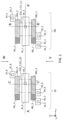
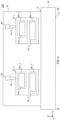
- FIG. 1 is a plan view of an integrated circuit device according to some embodiments of the present invention.
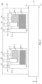
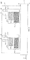
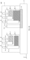
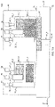
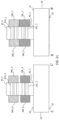
- FIGS. 2 and 3 are side views of an integrated circuit device 110 from viewpoints V and W in FIG. 1 , respectively, according to some embodiments of the present invention.
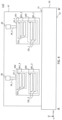
- FIGS. 4 and 5 are cross-sectional views of the integrated circuit device 110 taken along the line A-A' and the line B-B' in FIG. 1 , respectively, according to some embodiments of the present invention.
- the integrated circuit device 110 may include a stacked transistor structure ST on a substrate 10 and a diode structure DS.
- the substrate 10 may include a first surface S1 and a second surface S2.
- the first surface S1 and the second surface S2 may be opposite and parallel to each other.
- the first surface S1 may be a front side of the substrate 10, and the second surface S2 may be a backside of the substrate 10.
- the diode structure DS may include a first lower semiconductor layer 26L_1 and a second lower semiconductor layer 26L 2 that may be spaced apart from the first lower semiconductor layer 26L_1 in a first direction D1.
- the first direction D1 may be parallel to the first surface S1 and the second surface S2 of the substrate 10 and may be a first horizontal direction.
- a first lower thin semiconductor layer 22L_1 may be provided between the first lower semiconductor layer 26L_1 and the second lower semiconductor layer 26L 2 and may contact both the first lower semiconductor layer 26L_1 and the second lower semiconductor layer 26L 2.
- the first lower thin semiconductor layer 22L_1 may contact side surfaces of the first lower semiconductor layer 26L_1 and the second lower semiconductor layer 26L 2 as illustrated in FIG. 5 .
- the first lower semiconductor layer 26L_1 and the second lower semiconductor layer 26L_2 may have a first conductivity type (e.g., an N-type conductivity or a P-type conductivity).
- the diode structure DS may also include a first upper semiconductor layer 26U_1 and a second upper semiconductor layer 26U 2 that may be spaced apart from the first upper semiconductor layer 26U_1 in the first direction D1.
- a first upper thin semiconductor layer 22U_1 may be provided between the first upper semiconductor layer 26U_1 and the second upper semiconductor layer 26U 2 and may contact both the first upper semiconductor layer 26U_1 and the second upper semiconductor layer 26U 2.
- the first upper thin semiconductor layer 22U_1 may contact side surfaces of the first upper semiconductor layer 26U_1 and the second upper semiconductor layer 26U 2 as illustrated in FIG. 5 .
- the first upper semiconductor layer 26U_1 and the second upper semiconductor layer 26U 2 may have a second conductivity type that may be different from the first conductivity type.
- the first lower semiconductor layer 26L_1 may contact the first upper semiconductor layer 26U_1, and the first lower semiconductor layer 26L_1 and the first upper semiconductor layer 26U_1 may form a single diode. In some embodiments, an upper surface of the first lower semiconductor layer 26L_1 may contact a lower surface of the first upper semiconductor layer 26U_1 as illustrated in FIG. 2 .
- a lower surface of an element A (or similar language) means a surface of the element A facing the substrate 10.
- a first contact 32 1 that may contact the first lower semiconductor layer 26L_1 and a second contact 32 2 that may contact the first upper semiconductor layer 26U_1 may also be provided.
- the first contact 32 1 may contact a side surface of the first lower semiconductor layer 26L_1, and the second contact 32 2 may contact a side surface of the first upper semiconductor layer 26U_1 as illustrated in FIG. 1 but the present invention is not limited thereto.
- the first contact 32 1 may contact an upper surface of the first lower semiconductor layer 26L_1, and the second contact 32 2 may contact an upper surface of the first upper semiconductor layer 26U 1.
- the first contact 32 1 and the second contact 32 2 may contact portions of the diode, respectively. Accordingly, the first contact 32 1 and the second contact 32 2 may be a first diode contact and a second diode contact, respectively.
- the second lower semiconductor layer 26L 2 may contact the second upper semiconductor layer 26U 2.
- an upper surface of the second lower semiconductor layer 26L 2 may contact a lower surface of the second upper semiconductor layer 26U 2 as illustrated in FIG. 3 .
- a fourth contact 32 4 that may contact both the second lower semiconductor layer 26L 2 and the second upper semiconductor layer 26U 2 may be provided.
- the second lower semiconductor layer 26L 2, the second upper semiconductor layer 26U 2 and the fourth contact 32 4 may be omitted.
- a first metal layer 24_1 may be provided between the first lower semiconductor layer 26L_1 and the second lower semiconductor layer 26L 2 and between the first upper semiconductor layer 26U_1 and the second upper semiconductor layer 26U 2.
- the first metal layer 24_1 may be spaced apart from the first lower semiconductor layer 26L_1, the second lower semiconductor layer 26L 2, the first upper semiconductor layer 26U_1 and the second upper semiconductor layer 26U 2 in the first direction D1 as illustrated in FIGS. 1 and 5 .
- a portion of the first lower thin semiconductor layer 22L_1 and a portion of the first upper thin semiconductor layer 22U_1 may be in the first metal layer 24_1 as illustrated in FIGS. 1 and 4 .
- the first metal layer 24_1 may extend in the second direction D2 and surround the portion of the first lower thin semiconductor layer 22L_1 and the portion of the first upper thin semiconductor layer 22U_1.
- an insulating layer may be provided between the portion of the first lower thin semiconductor layer 22L_1 and the first metal layer 24 1 and between the portion of the first upper thin semiconductor layer 22U_1 and the first metal layer 24 1.
- FIG. 1 illustrates that the stacked transistor structure ST is spaced apart from the diode structure DS in a second direction D2, but the present invention is not limited thereto.
- the second direction D2 may be parallel to the first surface S1 and the second surface S2 of the substrate 10 and may be a second horizontal direction.
- the stacked transistor structure ST may be spaced apart from the diode structure DS in the first direction D1 or in a direction that may be different from the first direction D1 and the second direction D2.
- the first surface S1 and the second surface S2 of the substrate 10 may be spaced apart from each other in a third direction D3 that may be perpendicular to the first surface S1 and the second surface S2 of the substrate 10 and may be a vertical direction.
- the stacked transistor structure ST may include a third lower semiconductor layer 26L 3 and a fourth lower semiconductor layer 26L 4 that may be spaced apart from the third lower semiconductor layer 26L 3 in the first direction D1.
- a second lower thin semiconductor layer 22L 2 may be provided between the third lower semiconductor layer 26L 3 and the fourth lower semiconductor layer 26L 4 and may contact both the third lower semiconductor layer 26L 3 and the fourth lower semiconductor layer 26L 4.
- the second lower thin semiconductor layer 22L 2 may contact side surfaces of the third lower semiconductor layer 26L 3 and the fourth lower semiconductor layer 26L 4.
- the third lower semiconductor layer 26L 3 and the fourth lower semiconductor layer 26L 4 may have the first conductivity type (e.g., an N-type conductivity or a P-type conductivity).
- the second lower thin semiconductor layer 22L 2 may be a lower active layer of a lower transistor, and the third lower semiconductor layer 26L 3 and the fourth lower semiconductor layer 26L 4 may be lower source/drain regions of the lower transistor.
- the stacked transistor structure ST may also include a third upper semiconductor layer 26U 3 and a fourth upper semiconductor layer 26U 4 that may be spaced apart from the third upper semiconductor layer 26U 3 in the first direction D1.
- a second upper thin semiconductor layer 22U 2 may be provided between the third upper semiconductor layer 26U 3 and the fourth upper semiconductor layer 26U 4 and may contact both the third upper semiconductor layer 26U 3 and the fourth upper semiconductor layer 26U 4.
- the second upper thin semiconductor layer 22U 2 may contact side surfaces of the third upper semiconductor layer 26U 3 and the fourth upper semiconductor layer 26U 4.
- the third upper semiconductor layer 26U 3 and the fourth upper semiconductor layer 26U 4 may have the second conductivity type.
- the second upper thin semiconductor layer 22U 2 may be an upper active layer of an upper transistor, and the third upper semiconductor layer 26U 3 and the fourth upper semiconductor layer 26U 4 may be upper source/drain regions of the upper transistor.
- the third lower semiconductor layer 26L 3 and the third upper semiconductor layer 26U 3 may be spaced apart from each other in the third direction D3, and the fourth lower semiconductor layer 26L 4 and the fourth upper semiconductor layer 26U 4 may be spaced apart from each other in the third direction D3.
- the stacked transistor structure ST may further include a fifth contact 32 5, a sixth contact 32_6, an eighth contact 32 8 and a second metal layer 24 2.
- the fifth contact 32 5 and the sixth contact 32 6 may contact the third lower semiconductor layer 26L 3 and the third upper semiconductor layer 26U 3, respectively, and the eighth contact 32 8 may contact both the fourth lower semiconductor layer 26L 4 and the fourth upper semiconductor layer 26U 4.
- the second metal layer 24_2 may be provided between the third lower semiconductor layer 26L 3 and the fourth lower semiconductor layer 26L 4 and between the third upper semiconductor layer 26U 3 and the fourth upper semiconductor layer 26U 4.
- the second metal layer 24 2 may be spaced apart from the third lower semiconductor layer 26L 3, the fourth lower semiconductor layer 26L 4, the third upper semiconductor layer 26U 3 and the fourth upper semiconductor layer 26U 4 in the first direction D1 as illustrated in FIG. 1 .
- a portion of the second lower thin semiconductor layer 22L 2 and a portion of the second upper thin semiconductor layer 22U 2 may be in the second metal layer 24 2 as illustrated in FIGS. 1 and 4 .
- the second metal layer 24 2 may extend in the second direction D2 and surround the portion of the second lower thin semiconductor layer 22L 2 and the portion of the second upper thin semiconductor layer 22U 2.
- the second metal layer 24 2 may be a layer of a gate electrode.
- an insulating layer i.e., a gate insulating layer
- a first upper surface US 1 of the first upper thin semiconductor layer 22U_1 may be coplanar with a second upper surface US 2 of the second upper thin semiconductor layer 22U 2, and the first upper thin semiconductor layer 22U_1 and the second upper thin semiconductor layer 22U 2 may have an equal thickness in the third direction D3 as illustrated in FIG. 4 .
- a third upper surface US3 of the first lower thin semiconductor layer 22L_1 may be coplanar with a fourth upper surface US4 of the second lower thin semiconductor layer 22L 2, and the first lower thin semiconductor layer 22L_1 and the second lower thin semiconductor layer 22L 2 may have an equal thickness in the third direction D3 as illustrated in FIG. 4 .
- the first upper semiconductor layer 26U_1, the first lower semiconductor layer 26L_1, the third upper semiconductor layer 26U 3, the third lower semiconductor layer 26L 3 are represented by dotted boxes to show spatial relationships of those with other elements.
- each of the first upper semiconductor layer 26U_1, the first lower semiconductor layer 26L_1, the third upper semiconductor layer 26U 3, and the third lower semiconductor layer 26L 3 may overlap the entirety of a corresponding thin semiconductor layer in the first direction D1 as illustrated in FIG. 4 .
- the first upper semiconductor layer 26U_1 may overlap the entirety of the first upper thin semiconductor layer 22U_1.
- "an element A overlapping an element B in a direction X" means that there is at least one line that extends in the direction X and intersects both the elements A and B.
- each of the first metal layer 24 1 and the second metal layer 24_2 is illustrated in a single layer, the present invention is not limited thereto.
- each of the first metal layer 24_1 and the second metal layer 24 2 may include multiple layers.
- a lower portion of each of the first metal layer 24_1 and the second metal layer 24 2 may include material(s) different from an upper portion of each of the first metal layer 24 1 and the second metal layer 24 2.
- an isolation layer may be provided between the lower portion and the upper portion of each of the first metal layer 24 1 and the second metal layer 24 2, and the lower portion may be electrically isolated from the upper portion.
- the integrated circuit device 110 may further include first to eighth conductive vias 34_1, 34 2, 34 3, 34 4, 34 5, 34 6, 34 7 and 34 8 that may contact the first contact 32 1, the second contact 32 2, the first metal layer 24 1, the fourth contact 32 4, the fifth contact 32 5, the sixth contact 32 6, the second metal layer 24 2, the eighth contact 32_8, respectively.
- the first to eighth conductive vias 34 1, 34 2, 34 3, 34 4, 34 5, 34 6, 34 7 and 34_8 may be electrically connected to conductive wires 36, respectively.
- the first to eighth conductive vias 34 1, 34 2, 34 3, 34 4, 34 5, 34 6, 34 7 and 34_8 may contact the conductive wires 36, respectively, as illustrated in FIG. 2 and 3 .
- An interlayer insulating layer 42 may be provided on the substrate 10. Although the interlayer insulating layer 42 is illustrated as a single layer, the interlayer insulating layer 42 may include multiple layers stacked on the substrate 10. The diode structure DS and the stacked transistor structure ST may be provided in the interlayer insulating layer 42.
- the interlayer insulating layer 42 may include an insulating material (e.g., silicon oxide, silicon nitride, silicon oxynitride, silicon carbide and/or low-k material).
- the low k material may include, for example, fluorine-doped silicon dioxide, organosilicate glass, carbon-doped oxide, porous silicon dioxide, porous organosilicate glass, spin-on organic polymeric dielectrics, or spin-on silicon based polymeric dielectric.
- the substrate 10 may include one or more semiconductor materials, for example, Si, Ge, SiGe, GaP, GaAs, SiC, SiGeC and/or InP.
- the substrate 10 may be a bulk substrate (e.g., a bulk silicon substrate) or a semiconductor on insulator (SOI) substrate.
- Each of the first lower thin semiconductor layer 22L_1, the first upper thin semiconductor layer 22U_1, the second lower thin semiconductor layer 22L 2 and the second upper thin semiconductor layer 22U 2 may include multiple thin semiconductor layers stacked in the third direction D3.
- the first upper thin semiconductor layer 22U_1 may include two thin semiconductor layers as illustrated in FIGS. 4 and 5 but the present invention is not limited thereto.
- Each of the stacked thin semiconductor layers may be a nanosheet.
- the nanosheet may include semiconductor material(s) (e.g., silicon, germanium, silicon-germanium, and/or III-V semiconductor compound).
- each of nanosheets may have a thickness in a range of, for example, from 1 nm to 100 nm in the third direction D3.
- the first and second metal layers 24_1 and 24_2 may include a semiconductor layer (e.g., a poly silicon layer), a work function layer (e.g., TiC layer, TiAl layer, TiAlC layer or TiN layer) and/or a metal layer (e.g., a tungsten layer, an aluminum layer or a copper layer).
- a semiconductor layer e.g., a poly silicon layer
- a work function layer e.g., TiC layer, TiAl layer, TiAlC layer or TiN layer
- a metal layer e.g., a tungsten layer, an aluminum layer or a copper layer.
- Each of the first to fourth lower semiconductor layers 26L 1, 26L 2, 26L 3 and 26L 4 and the first to fourth upper semiconductor layers 26U_1, 26U 2, 26U 3 and 26U 4 may include semiconductor material(s) (e.g., silicon, germanium, silicon-germanium) and may also include optionally dopants (e.g., B, P or As).
- the first lower semiconductor layer 26L_1 and the first upper semiconductor layer 26U_1 may be a silicon layer (e.g., an amorphous silicon layer).
- the first contact 32 1, the second contact 32 2, the fourth contact 32 4, the fifth contact 34 5, the sixth contact 32_6, the eighth contact 32 8, the first to eighth conductive vias 34 1, 34 2, 34 3, 34 4, 34 5, 34 6, 34 7 and 34 8, and the conductive wires 36 may include a metal layer (e.g., a ruthenium layer, a molybdenum layer, a copper layer, a cobalt layer, an aluminum layer and/or a tungsten layer) and/or a metal nitride layer (e.g., a titanium nitride layer and/or a tantalum nitride layer).
- a metal layer e.g., a ruthenium layer, a molybdenum layer, a copper layer, a cobalt layer, an aluminum layer and/or a tungsten layer
- a metal nitride layer e.g., a titanium nitride layer and/or a tantalum nitride layer
- FIGS. 6 and 7 are cross-sectional views of an integrated circuit device 120 taken along the line A-A' and the line B-B' in FIG. 1 , respectively, according to some embodiments of the present invention.
- the integrated circuit device 120 may be similar to the integrated circuit device 110 with a primary difference being that each of the first lower thin semiconductor layer 22L_1, the first upper thin semiconductor layer 22U_1, the second lower thin semiconductor layer 22L 2, the second upper thin semiconductor layer 22U 2 is a single layer (e.g., a single nanosheet).
- FIGS. 8 and 9 are side views of an integrated circuit device 130 from viewpoints V and W in FIG. 1 , respectively, according to some embodiments of the present invention.
- the integrated circuit device 130 may be similar to the integrated circuit device 110 with a primary difference being that a first intrinsic semiconductor layer 52 is provided between the first lower semiconductor layer 26L_1 and the first upper semiconductor layer 26U_1 and contacts both the first lower semiconductor layer 26L_1 and the first upper semiconductor layer 26U_1.
- the first lower semiconductor layer 26L_1, the first intrinsic semiconductor layer 52 and the first upper semiconductor layer 26U_1 may collectively form a single diode.
- the integrated circuit device 130 may also include a second intrinsic semiconductor layer 54 that may be provided between the second lower semiconductor layer 26L 2 and the second upper semiconductor layer 26U 2 and contacts both the second lower semiconductor layer 26L 2 and the second upper semiconductor layer 26U 2.
- the first intrinsic semiconductor layer 52 and the second intrinsic semiconductor layer 54 may include silicon and/or silicon germanium and may have a thickness in a range of 10 nm to 200 nm in the third direction D3.
- FIGS. 10 and 11 are side views of an integrated circuit device 140 from viewpoints V and W in FIG. 1 , respectively, according to some embodiments of the present invention.
- the integrated circuit device 140 may be similar to the integrated circuit device 110 with primary differences being that the first lower semiconductor layer 26L_1 contacts a first portion 62 of the substrate 10.
- the first lower semiconductor layer 26L_1 and the first portion 62 of the substrate 10 may form a single diode.
- the first portion 62 of the substrate 10 may have the second conductivity type.
- a ninth contact 32_9 may be provided in the interlayer insulating layer 42 and may contact the first portion 62 of the substrate 10.
- the first contact 32 1 and the ninth contact 32_9 may be a first diode contact and a second diode contact, respectively.
- the first portion 62 of the substrate 10 may include dopants at a concentration in a range of 10 13 cm -3 to 10 20 cm -3 .
- the first portion 62 of the substrate 10 may have a thickness in a range of about 10 nm to about 400 nm (e.g., about 100 nm to about 200 nm) in the third direction D3.
- the ninth contact 32 9 may include a metal layer (e.g., a ruthenium layer, a molybdenum layer, a copper layer, a cobalt layer, an aluminum layer and/or a tungsten layer) and/or a metal nitride layer (e.g., a titanium nitride layer and/or a tantalum nitride layer).
- FIG. 10 illustrates that the first upper semiconductor layer 26U_1 contacts the first lower semiconductor layer 26L_1, in some embodiments, the first upper semiconductor layer 26U_1 may be spaced apart from the first lower semiconductor layer 26L_1 in the third direction D3. Further, in some embodiments, the second upper semiconductor layer 26U 2 may contact the second lower semiconductor layer 26L 2 as illustrated in FIG. 11 or the second upper semiconductor layer 26U 2 may be spaced apart from the second lower semiconductor layer 26L 2 in the third direction D3.
- FIG. 12 is a side view of an integrated circuit device 150 from viewpoint V in FIG. 1 according to some embodiments of the present invention.
- the integrated circuit device 150 may be similar to the integrated circuit device 140 with primary differences being that a third intrinsic semiconductor layer 56 is provided between the first portion 62 of the substrate 10 and the first lower semiconductor layer 26L_1 and contacts both the first portion 62 of the substrate 10 and the first lower semiconductor layer 26L_1.
- the first lower semiconductor layer 26L_1, the third intrinsic semiconductor layer 56, and the first portion 62 of the substrate 10 may collectively form a single diode.
- FIG. 13 is a side view of an integrated circuit device 160 from viewpoint V in FIG. 1 according to some embodiments of the present invention.
- the integrated circuit device 160 may be similar to the integrated circuit device 140 with a primary difference being that the ninth contact 32 9 is in the substrate 10.
- the ninth contact 32 9 includes a surface 32 9S that may be coplanar with the second surface S2 of the substrate 10 as illustrated in FIG. 13 .
- the surface 32 9S of the ninth contact 32_9 may protrude outwardly in the third direction D3 beyond the second surface S2 of the substrate 10 or may be recessed with respect to the second surface S2 of the substrate 10.
- FIG. 14 is a side view of an integrated circuit device 170 from viewpoint V in FIG. 1 according to some embodiments of the present invention.
- the integrated circuit device 170 may be similar to the integrated circuit device 150 with primary differences being that a second portion 64 of the substrate 10 and a tenth contact 32 10 may be additionally provided.
- the second portion 64 of the substrate 10 may have a conductivity type (i.e., the first conductivity type) that is different from the first portion 62 of the substrate 10, and the first portion 62 and the second portion 64 of the substrate 10 may form a single diode.
- the ninth contact 32 9 and the tenth contact 32_10 may be a first diode contact and a second diode contact, respectively.
- the second portion 64 of the substrate 10 may include dopants at a concentration in a range of 10 13 cm -3 to 10 20 cm -3 .
- the second portion 64 of the substrate 10 may have a thickness in a range of about 10 nm to about 400 nm (e.g., about 100 nm to about 300 nm) in the third direction D3.
- the tenth contact 32_10 may include a metal layer (e.g., a ruthenium layer, a molybdenum layer, a copper layer, a cobalt layer, an aluminum layer and/or a tungsten layer) and/or a metal nitride layer (e.g., a titanium nitride layer and/or a tantalum nitride layer).
- FIG. 15 is a side view of an integrated circuit device 180 from viewpoint V in FIG. 1 according to some embodiments of the present invention.
- the integrated circuit device 180 may be similar to the integrated circuit device 170 with primary differences being that the first lower semiconductor layer 26L_1 is spaced apart from the substrate 10 in the third direction D3 and the first upper semiconductor layer 26U_1 is spaced apart from the first lower semiconductor layer 26L 1 in the third direction D3.
- FIG. 16 is a side view of an integrated circuit device 190 from viewpoint V in FIG. 1 according to some embodiments of the present invention.
- the integrated circuit device 190 may be similar to the integrated circuit device 180 with a primary difference being that the tenth contact 32 10 is in the substrate 10.
- the tenth contact 32 10 includes a surface 32_10S that may be coplanar with the second surface S2 of the substrate 10 as illustrated in FIG. 16 .
- the surface 32_10S of the tenth contact 32 10 may protrude outwardly in the third direction D3 beyond the second surface S2 of the substrate 10 or may be recessed with respect to the second surface S2 of the substrate 10.
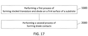
- FIGS. 17 and 18 are flow charts of methods of forming an integrated circuit device according to some embodiments of the present invention.
- FIGS. 19-21 are cross-sectional views taken along the line B-B' and the line C-C' in FIG. 1 illustrating methods of forming an integrated circuit device according to some embodiments of the present invention.
- the methods may include performing a first process of forming stacked transistors and a diode on a first surface of a substrate (Block 1000) and performing a second process of forming diode contacts (Block 2000).
- the first process of forming stacked transistors and a diode may include forming a lower thin semiconductor layer 22L_1 and a lower active layer 22L 2 on a substrate 10 (Block 1100).
- the lower thin semiconductor layer 22L_1 and the lower active layer 22L 2 may be formed concurrently at the same height from the first surface S1 of the substrate 10.
- a preliminary lower semiconductor layer may be formed on the substrate 10 and then the preliminary lower semiconductor layer may be patterned, thereby forming the lower thin semiconductor layer 22L_1 and the lower active layer 22L 2.
- the lower thin semiconductor layer 22L_1 and the lower active layer 22L 2 may be portions of the single preliminary lower semiconductor layer.
- a first interlayer insulating layer 42_1 may be formed on the lower thin semiconductor layer 22L_1 and the lower active layer 22L 2 and may expose opposing side surfaces of the lower thin semiconductor layer 22L_1 and the lower active layer 22L_2.
- a lower semiconductor layer e.g., first and second lower semiconductor layers 26L_1 and 26L 2 and a lower source/drain region (e.g., third and fourth lower source/drain regions 26L 3 and 26L 4) may be formed (Block 1200).
- the first and second lower semiconductor layers 26L_1 and 26L 2 may be formed by an epitaxial growth process using the lower thin semiconductor layer 22L_1 as a seed layer
- the third and fourth lower source/drain regions 26L 3 and 26L 4 may be formed by an epitaxial growth process using the lower active layer 22L 2 as a seed layer.
- the first and second lower semiconductor layers 26L_1 and 26L 2 and the third and fourth lower source/drain regions 26L 3 and 26L 4 may be formed by a single epitaxial growth process.
- Opposing side surfaces of the lower thin semiconductor layer 22L_1 may contact the first and second lower semiconductor layers 26L_1 and 26L 2, respectively, and opposing side surfaces of the lower active layer 22L 2 may contact the third and fourth lower source/drain regions 26L 3 and 26L 4, respectively, as illustrated in FIG. 20 .
- an upper thin semiconductor layer 22U_1 and an upper active layer 22U 2 may be formed on the lower thin semiconductor layer 22L_1 and the lower active layer 22L 2, respectively (Block 1300).
- a second interlayer insulating layer 42_2 may be formed on the upper thin semiconductor layer 22U_1 and the upper active layer 22U 2 and may expose opposing side surfaces of the upper thin semiconductor layer 22U_1 and the upper active layer 22U_2.
- An upper semiconductor layer e.g., first and second upper semiconductor layers 26U_1 and 26U 2 and an upper source/drain region (e.g., third and fourth source/drain regions 26U 3 and 26U 4) may be formed (Block 1400).
- the first and second upper semiconductor layers 26U_1 and 26U 2 may be formed by an epitaxial growth process using the upper thin semiconductor layer 22U_1 as a seed layer
- the third and fourth source/drain regions 26U 3 and 26U 4 may be formed by an epitaxial growth process using the upper active layer 22U 2 as a seed layer.
- the first and second upper semiconductor layers 26U_1 and 26U 2 and the third and fourth source/drain regions 26U 3 and 26U 4 may be formed by a single epitaxial growth process.
- the first and second interlayer insulating layers 42 1 and 42 2 may be removed and a first metal layer 24 1 and a second metal layer 24 2 may be formed (Block 1500).
- an insulating layer (not shown) may be formed on exposed surfaces of the lower thin semiconductor layer 22L_1, the lower active layer 22L 2, the upper thin semiconductor layer 22U_1, and the upper active layer 22U 2.
- FIG. 22 is a flow chart of the second process of forming diode contacts according to some embodiments of the present invention
- FIG. 23 is a cross-sectional view illustrating the second process.
- the second process may include forming a first diode contact (e.g., the first contact 32 1 in FIG. 13 or the ninth contact 32 9 in FIG. 16 ) (Block 2100), and then performing a thinning process on the second surface S2 of the substrate 10 (Block 2200).
- the thinning process may include an etch process (e.g., a dry etch process and/or a wet etch process) and/or a grinding process.
- a second diode contact (e.g., the ninth contact 32_9 in FIG. 13 or the tenth contact 32 10 in FIG. 16 ) may be formed in the substrate 10 (Block 2300).
- the second diode contact may be formed by etching a portion of the substrate 10 from the second surface S2 of the substrate 10 to form an opening 31 and then forming the second diode contact in the opening 31.
- the opening 31 may extend into the substrate 10 from the second surface S2, and a first portion 62 or a second portion 64 of the substrate 10 may be exposed at a bottom of the opening 31.
- the ninth contact 32 9 shown in FIG. 13 may be formed in the opening 31.
- the tenth contact 32 10 shown in FIG. 16 may be formed in the opening 31.
- the second process of forming diode contacts according to some embodiments of the present invention may not include a thinning process (Block 2200 in FIG. 22 ), and both the first diode contact (e.g., the first contact 32 1 in FIGS. 2 and 10 or the ninth contact 32 9 in FIG. 14 ) and the second diode contact (e.g., the second contact 32 2 in FIG. 2 , the ninth contact 32 9 in FIG. 10 or the tenth contact 32 10 in FIG. 14 ) may be formed on the first surface S1 (e.g., a front side) of the substrate 10 after the first metal layer 24_1 and the second metal layer 24 2 are formed.
- first diode contact e.g., the first contact 32 1 in FIGS. 2 and 10 or the ninth contact 32 9 in FIG. 14
- the second diode contact e.g., the second contact 32 2 in FIG. 2 , the ninth contact 32 9 in FIG. 10 or the tenth contact 32 10 in FIG. 14
- the first surface S1
- Example embodiments of the present invention are described herein with reference to cross-sectional views that are schematic illustrations of idealized embodiments and intermediate structures of example embodiments. As such, variations from the shapes of the illustrations as a result, for example, of manufacturing techniques and/or tolerances, are to be expected. Thus, example embodiments of the present invention should not be construed as limited to the particular shapes illustrated herein but include deviations in shapes that result, for example, from manufacturing, unless the context clearly indicates otherwise.
Landscapes
- Semiconductor Integrated Circuits (AREA)
- Metal-Oxide And Bipolar Metal-Oxide Semiconductor Integrated Circuits (AREA)
Applications Claiming Priority (2)
| Application Number | Priority Date | Filing Date | Title |
|---|---|---|---|
| US202163246965P | 2021-09-22 | 2021-09-22 | |
| US17/554,171 US11764207B2 (en) | 2021-09-22 | 2021-12-17 | Diode structures of stacked devices and methods of forming the same |
Publications (2)
| Publication Number | Publication Date |
|---|---|
| EP4156271A2 true EP4156271A2 (de) | 2023-03-29 |
| EP4156271A3 EP4156271A3 (de) | 2023-06-07 |
Family
ID=83457152
Family Applications (1)
| Application Number | Title | Priority Date | Filing Date |
|---|---|---|---|
| EP22194108.1A Pending EP4156271A3 (de) | 2021-09-22 | 2022-09-06 | Diodenstrukturen von gestapelten vorrichtungen und ihre herstellungsverfahren |
Country Status (5)
| Country | Link |
|---|---|
| US (2) | US11764207B2 (de) |
| EP (1) | EP4156271A3 (de) |
| KR (1) | KR20230042616A (de) |
| CN (1) | CN115939133A (de) |
| TW (1) | TW202333343A (de) |
Cited By (1)
| Publication number | Priority date | Publication date | Assignee | Title |
|---|---|---|---|---|
| EP4510190A1 (de) * | 2023-08-14 | 2025-02-19 | Samsung Electronics Co., Ltd. | Integrierte schaltungsvorrichtungen mit entladungsstrecke und entsprechende herstellungsverfahren |
Families Citing this family (4)
| Publication number | Priority date | Publication date | Assignee | Title |
|---|---|---|---|---|
| US20240096949A1 (en) * | 2022-09-15 | 2024-03-21 | International Business Machines Corporation | Diodes in nanosheet technology |
| US20240332131A1 (en) * | 2023-03-29 | 2024-10-03 | Samsung Electronics Co., Ltd. | Integrated circuit devices including stacked transistors and methods of forming the same |
| US20240429226A1 (en) * | 2023-06-20 | 2024-12-26 | International Business Machines Corporation | Protection diode for stacked field effect transistor |
| US12087669B1 (en) * | 2023-08-14 | 2024-09-10 | Samsung Electronics Co., Ltd. | Integrated circuit devices including discharging path and methods of forming the same |
Family Cites Families (10)
| Publication number | Priority date | Publication date | Assignee | Title |
|---|---|---|---|---|
| US20070023866A1 (en) | 2005-07-27 | 2007-02-01 | International Business Machines Corporation | Vertical silicon controlled rectifier electro-static discharge protection device in bi-cmos technology |
| KR20110134160A (ko) | 2010-06-08 | 2011-12-14 | 삼성전자주식회사 | 비휘발성 메모리 소자의 제조 방법 |
| US9583490B2 (en) | 2015-01-20 | 2017-02-28 | Taiwan Semiconductor Manufacturing Company, Ltd. | Inverters and manufacturing methods thereof |
| US9431388B1 (en) | 2015-04-29 | 2016-08-30 | Globalfoundries Inc. | Series-connected nanowire structures |
| US9997463B2 (en) | 2015-07-01 | 2018-06-12 | Stmicroelectronics, Inc. | Modular interconnects for gate-all-around transistors |
| WO2017105515A1 (en) | 2015-12-18 | 2017-06-22 | Intel Corporation | Stacked transistors |
| JP6700565B2 (ja) | 2016-06-10 | 2020-05-27 | 株式会社ソシオネクスト | 半導体装置 |
| US10276714B2 (en) | 2017-08-09 | 2019-04-30 | International Business Machines Corporation | Twin gate field effect diode |
| CN111386606A (zh) | 2018-01-18 | 2020-07-07 | 英特尔公司 | 堆叠晶体管架构中的垂直二极管 |
| US11605565B2 (en) | 2018-12-28 | 2023-03-14 | Intel Corporation | Three dimensional integrated circuits with stacked transistors |
-
2021
- 2021-12-17 US US17/554,171 patent/US11764207B2/en active Active
-
2022
- 2022-03-30 KR KR1020220039903A patent/KR20230042616A/ko active Pending
- 2022-09-06 EP EP22194108.1A patent/EP4156271A3/de active Pending
- 2022-09-16 TW TW111135069A patent/TW202333343A/zh unknown
- 2022-09-16 CN CN202211131804.6A patent/CN115939133A/zh active Pending
-
2023
- 2023-08-07 US US18/366,010 patent/US12094869B2/en active Active
Cited By (1)
| Publication number | Priority date | Publication date | Assignee | Title |
|---|---|---|---|---|
| EP4510190A1 (de) * | 2023-08-14 | 2025-02-19 | Samsung Electronics Co., Ltd. | Integrierte schaltungsvorrichtungen mit entladungsstrecke und entsprechende herstellungsverfahren |
Also Published As
| Publication number | Publication date |
|---|---|
| US20230092061A1 (en) | 2023-03-23 |
| US12094869B2 (en) | 2024-09-17 |
| US11764207B2 (en) | 2023-09-19 |
| TW202333343A (zh) | 2023-08-16 |
| US20230378164A1 (en) | 2023-11-23 |
| KR20230042616A (ko) | 2023-03-29 |
| CN115939133A (zh) | 2023-04-07 |
| EP4156271A3 (de) | 2023-06-07 |
Similar Documents
| Publication | Publication Date | Title |
|---|---|---|
| EP4156271A2 (de) | Diodenstrukturen von gestapelten vorrichtungen und ihre herstellungsverfahren | |
| TWI433305B (zh) | Soi裝置及其製造之方法 | |
| US20230369218A1 (en) | Interlevel via for stacked field-effect transistor device | |
| US20200381420A1 (en) | Recessed composite capacitor | |
| US12230571B2 (en) | Integrated circuit devices including a power rail and methods of forming the same | |
| KR20240123661A (ko) | 반도체 소자 및 그의 제조 방법 | |
| US20250221030A1 (en) | Stacked forksheet transistors | |
| US20240421154A1 (en) | Integrated circuit devices including a backside power distribution network structure and methods of forming the same | |
| US20200020770A1 (en) | Composite spacers for tailoring the shape of the source and drain regions of a field-effect transistor | |
| CN120917901A (zh) | 用于背侧电源应用的背侧电源岛 | |
| US12317582B2 (en) | Integrated circuit devices including a metal resistor and methods of forming the same | |
| US20250015157A1 (en) | Semiconductor device and method of fabricating the same | |
| US7465639B1 (en) | Method for fabricating an SOI device | |
| US20240321687A1 (en) | Backside decoupling capacitor integration with backside contact | |
| JP2024159473A (ja) | 半導体素子及びその製造方法 | |
| US12249603B2 (en) | Resistor structures of integrated circuit devices including stacked transistors and methods of forming the same | |
| US12604492B2 (en) | Semiconductor device including an active pattern | |
| US20250293161A1 (en) | Semiconductor device with source/drain contact mol cut structure | |
| US12453178B2 (en) | IC structure for connected capacitances and method of forming same | |
| US20240341101A1 (en) | Semiconductor device and method for transistor memory element | |
| US20250386589A1 (en) | Stacked nanosheet capacitor-transistor device | |
| US20260114025A1 (en) | Diode structures of stacked transistors and methods of manufacturing the same | |
| US20250287645A1 (en) | Fork sheet transistor with via-to-backside power rail structure | |
| US20260068135A1 (en) | Semiconductor structure and method of manufacturing the same | |
| US20250151345A1 (en) | Module-less nanosheet fets with direct backside contact |
Legal Events
| Date | Code | Title | Description |
|---|---|---|---|
| PUAI | Public reference made under article 153(3) epc to a published international application that has entered the european phase |
Free format text: ORIGINAL CODE: 0009012 |
|
| STAA | Information on the status of an ep patent application or granted ep patent |
Free format text: STATUS: THE APPLICATION HAS BEEN PUBLISHED |
|
| AK | Designated contracting states |
Kind code of ref document: A2 Designated state(s): AL AT BE BG CH CY CZ DE DK EE ES FI FR GB GR HR HU IE IS IT LI LT LU LV MC MK MT NL NO PL PT RO RS SE SI SK SM TR |
|
| PUAL | Search report despatched |
Free format text: ORIGINAL CODE: 0009013 |
|
| AK | Designated contracting states |
Kind code of ref document: A3 Designated state(s): AL AT BE BG CH CY CZ DE DK EE ES FI FR GB GR HR HU IE IS IT LI LT LU LV MC MK MT NL NO PL PT RO RS SE SI SK SM TR |
|
| RIC1 | Information provided on ipc code assigned before grant |
Ipc: H01L 29/775 20060101ALN20230503BHEP Ipc: H01L 27/092 20060101ALN20230503BHEP Ipc: H01L 29/868 20060101ALI20230503BHEP Ipc: H01L 29/861 20060101ALI20230503BHEP Ipc: H01L 29/06 20060101ALI20230503BHEP Ipc: H01L 29/66 20060101ALI20230503BHEP Ipc: H01L 27/07 20060101ALI20230503BHEP Ipc: H01L 27/06 20060101AFI20230503BHEP |
|
| P01 | Opt-out of the competence of the unified patent court (upc) registered |
Effective date: 20230520 |
|
| STAA | Information on the status of an ep patent application or granted ep patent |
Free format text: STATUS: REQUEST FOR EXAMINATION WAS MADE |
|
| 17P | Request for examination filed |
Effective date: 20230810 |
|
| RBV | Designated contracting states (corrected) |
Designated state(s): AL AT BE BG CH CY CZ DE DK EE ES FI FR GB GR HR HU IE IS IT LI LT LU LV MC MK MT NL NO PL PT RO RS SE SI SK SM TR |