EP4156514A1 - Elektronische vorrichtung mit einer photodiode und der fähigkeit zum umschalten zwischen lichterfassungsfunktion und lichtladefunktion - Google Patents
Elektronische vorrichtung mit einer photodiode und der fähigkeit zum umschalten zwischen lichterfassungsfunktion und lichtladefunktion Download PDFInfo
- Publication number
- EP4156514A1 EP4156514A1 EP22191784.2A EP22191784A EP4156514A1 EP 4156514 A1 EP4156514 A1 EP 4156514A1 EP 22191784 A EP22191784 A EP 22191784A EP 4156514 A1 EP4156514 A1 EP 4156514A1
- Authority
- EP
- European Patent Office
- Prior art keywords
- terminal
- energy storage
- electronic device
- switch
- voltage
- Prior art date
- Legal status (The legal status is an assumption and is not a legal conclusion. Google has not performed a legal analysis and makes no representation as to the accuracy of the status listed.)
- Withdrawn
Links
Images





Classifications
-
- H—ELECTRICITY
- H03—ELECTRONIC CIRCUITRY
- H03K—PULSE TECHNIQUE
- H03K17/00—Electronic switching or gating, i.e. not by contact-making and –breaking
- H03K17/51—Electronic switching or gating, i.e. not by contact-making and –breaking characterised by the components used
- H03K17/56—Electronic switching or gating, i.e. not by contact-making and –breaking characterised by the components used by the use, as active elements, of semiconductor devices
- H03K17/687—Electronic switching or gating, i.e. not by contact-making and –breaking characterised by the components used by the use, as active elements, of semiconductor devices the devices being field-effect transistors
- H03K17/693—Switching arrangements with several input- or output-terminals, e.g. multiplexers, distributors
-
- G—PHYSICS
- G01—MEASURING; TESTING
- G01J—MEASUREMENT OF INTENSITY, VELOCITY, SPECTRAL CONTENT, POLARISATION, PHASE OR PULSE CHARACTERISTICS OF INFRARED, VISIBLE OR ULTRAVIOLET LIGHT; COLORIMETRY; RADIATION PYROMETRY
- G01J1/00—Photometry, e.g. photographic exposure meter
- G01J1/42—Photometry, e.g. photographic exposure meter using electric radiation detectors
- G01J1/44—Electric circuits
-
- G—PHYSICS
- G06—COMPUTING OR CALCULATING; COUNTING
- G06V—IMAGE OR VIDEO RECOGNITION OR UNDERSTANDING
- G06V40/00—Recognition of biometric, human-related or animal-related patterns in image or video data
- G06V40/10—Human or animal bodies, e.g. vehicle occupants or pedestrians; Body parts, e.g. hands
- G06V40/12—Fingerprints or palmprints
- G06V40/13—Sensors therefor
- G06V40/1318—Sensors therefor using electro-optical elements or layers, e.g. electroluminescent sensing
-
- H—ELECTRICITY
- H02—GENERATION; CONVERSION OR DISTRIBUTION OF ELECTRIC POWER
- H02J—ELECTRIC POWER NETWORKS; CIRCUIT ARRANGEMENTS OR SYSTEMS FOR SUPPLYING OR DISTRIBUTING ELECTRIC POWER; SYSTEMS FOR STORING ELECTRIC ENERGY
- H02J50/00—Circuit arrangements or systems for wireless supply or distribution of electric power
- H02J50/001—Energy harvesting or scavenging
-
- H—ELECTRICITY
- H02—GENERATION; CONVERSION OR DISTRIBUTION OF ELECTRIC POWER
- H02J—ELECTRIC POWER NETWORKS; CIRCUIT ARRANGEMENTS OR SYSTEMS FOR SUPPLYING OR DISTRIBUTING ELECTRIC POWER; SYSTEMS FOR STORING ELECTRIC ENERGY
- H02J7/00—Circuit arrangements for charging or discharging batteries or for supplying loads from batteries
- H02J7/34—Parallel operation in networks using both storage and other DC sources, e.g. providing buffering
- H02J7/35—Parallel operation in networks using both storage and other DC sources, e.g. providing buffering with light sensitive cells
-
- H—ELECTRICITY
- H03—ELECTRONIC CIRCUITRY
- H03K—PULSE TECHNIQUE
- H03K17/00—Electronic switching or gating, i.e. not by contact-making and –breaking
- H03K17/94—Electronic switching or gating, i.e. not by contact-making and –breaking characterised by the way in which the control signals are generated
- H03K17/96—Touch switches
- H03K17/9627—Optical touch switches
-
- G—PHYSICS
- G01—MEASURING; TESTING
- G01J—MEASUREMENT OF INTENSITY, VELOCITY, SPECTRAL CONTENT, POLARISATION, PHASE OR PULSE CHARACTERISTICS OF INFRARED, VISIBLE OR ULTRAVIOLET LIGHT; COLORIMETRY; RADIATION PYROMETRY
- G01J1/00—Photometry, e.g. photographic exposure meter
- G01J1/42—Photometry, e.g. photographic exposure meter using electric radiation detectors
- G01J1/44—Electric circuits
- G01J2001/4446—Type of detector
- G01J2001/446—Photodiode
-
- H—ELECTRICITY
- H02—GENERATION; CONVERSION OR DISTRIBUTION OF ELECTRIC POWER
- H02J—ELECTRIC POWER NETWORKS; CIRCUIT ARRANGEMENTS OR SYSTEMS FOR SUPPLYING OR DISTRIBUTING ELECTRIC POWER; SYSTEMS FOR STORING ELECTRIC ENERGY
- H02J2207/00—Details of circuit arrangements for charging or discharging batteries or supplying loads from batteries
- H02J2207/50—Charging of capacitors, supercapacitors, ultra-capacitors or double layer capacitors
-
- H—ELECTRICITY
- H02—GENERATION; CONVERSION OR DISTRIBUTION OF ELECTRIC POWER
- H02J—ELECTRIC POWER NETWORKS; CIRCUIT ARRANGEMENTS OR SYSTEMS FOR SUPPLYING OR DISTRIBUTING ELECTRIC POWER; SYSTEMS FOR STORING ELECTRIC ENERGY
- H02J7/00—Circuit arrangements for charging or discharging batteries or for supplying loads from batteries
Definitions
- the disclosure is generally related to an electronic device having a sensing function and a charging function, and more particularly it is related to an electronic device having a photodiode and capable of switching between a light-sensing function and a light-charging function.
- sensing device in the current generation of electronic devices can also have the function of recharging the battery, then ambient light and the screen light can be converted into an electrical signal that can charge the battery, effectively prolonging the usage time of the electronic device and improving the convenience of charging it. In addition, this would contribute to a reduction in electricity bills and environmental pollution.
- An electronic device which includes a photodiode, a switching circuit, a readout circuit, and an energy storage device.
- the photodiode includes a first terminal and a second terminal and is configured to generate a signal according to a light.
- the switching circuit is electrically connected to the first terminal and the second terminal. When the electronic device operates in a sensing mode, the switching circuit electrically isolates the photodiode from the energy storage device so that the signal is provided to the readout circuit. When the electronic device operates in a charging mode, the switching circuit electrically connects the photodiode to the energy storage device so that the signal is provided to the energy storage device.
- first, second, third etc. may be used herein to describe various elements, components, regions, layers, portions and/or sections, these elements, components, regions, layers, portions and/or sections should not be limited by these terms. These terms are only used to distinguish one element, component, region, layer, portion or section from another region, layer or section. Thus, a first element, component, region, layer, portion or section discussed below could be termed a second element, component, region, layer, portion or section without departing from the teachings of the disclosure.
- a feature on, connected to, and/or coupled to another feature in the disclosure that follows may include embodiments in which the features are formed in direct contact, and may also include embodiments in which additional features may be formed interposing the features, such that the features may not be in direct contact.
- additional features may be formed interposing the features, such that the features may not be in direct contact.
- joining and connecting may also include the case where both structures are movable or both structures are fixed.
- the term “coupled” includes any direct and indirect electrical connection means.
- the electrical connection or coupling described in this disclosure may refer to direct connection or indirect connection.
- direct connection the terminals of two devices in a circuit are directly connected or connected to each other through a conducting line.
- indirectly connection there are switches, diodes, capacitors, inductors, resistors, other suitable components or a combination of the components mentioned above between the terminals of two devices in a circuit, but it is not limited thereto.
- the electronic device may include a display device, a backlight device, an antenna device, a sensing device or a splicing device, but is not limited thereto.
- the electronic device may be a bendable or flexible electronic device.
- the display device may be a non-self-luminous display device or a self-luminous display device.
- the antenna device may be a liquid crystal antenna device or a non-liquid-crystal antenna device, and the sensing device may be a sensing device for sensing capacitance, light, heat or ultrasonic waves, but it is not limited thereto.
- Electronic components may include passive and active components, such as capacitors, resistors, inductors, diodes, transistors, and the like.
- the diodes may include light-emitting diodes or light sensing diodes.
- the light-emitting diodes may, for example, include organic light-emitting diodes (OLEDs), sub-millimeter light-emitting diodes (mini LEDs), micro light-emitting diodes (micro LEDs), or quantum dot light-emitting diodes (quantum dot LED), but it is not limited thereto.
- the splicing device may be, for example, a display splicing device or an antenna splicing device, but it is not limited thereto.
- the electronic device can be any arrangement and combination of the foregoing, but it is not limited thereto.
- the disclosure will be described by taking the display device as the electronic device or the splicing device, but the disclosure is not limited thereto.
- Fig. 1 is a block diagram illustrating an electronic device in accordance with an embodiment of the disclosure.
- the electronic device 100 includes an energy storage device 110, a system board 120, a panel 130, and a sensing device 140.
- the energy storage device 110 is configured to store electrical energy POWER, and provides the stored electrical energy POWER to the system board 120.
- the energy storage device 110 may be a battery, a capacitor, or other device that can store electrical energy.
- the energy storage device 110 may be a solar cell.
- the system board 120 provides the electrical energy POWER provided by the energy storage device 110 to the panel 130 and the sensing device 140.
- the system board 120 and the panel 130 communicate to each other through the first data signal DT1, and the system board 120 communicates with the sensing device 140 through the second data signal DT2.
- the system board 120 includes a memory 121 and a processor 122.
- the memory 121 is configured to store the fingerprint of the user, and the processor 122 is configured to operate in the sensing mode or the charging mode according to whether the touch device 131 is triggered.
- the panel 130 includes a touch device 131 and a display 132, in which the display 132 has a display surface (not shown in the figure), the touch device 131 is located on the back side of the display surface, and the touch device 131 detects whether the display surface of the display 132 is touched.
- the sensing device 140 is disposed on the panel 130 and located on the back side of the display surface of the display 132.
- the sensing device 140 can sense light to generate the fingerprint information, and provide the generated fingerprint information to the processor 122 through the second data signal DT2.
- the fingerprint information can be generated as images or data.
- the sensing device 140 can also sense light to generate electrical energy POWER to charge the energy storage device 110.
- the sensing device 140 is a photodiode.
- the processor 122 when the touch device 131 detects that the display surface is touched, the processor 122 operates in a sensing mode to perform a fingerprint comparison, and the fingerprint information is compared with the user's fingerprint stored in the memory 121, in which the display surface of the display 132 can provide a light source.
- the processor 122 when the touch device 131 does not detect that the display surface is touched, the processor 122 operates in the charging mode, the sensing device 140 converts the received light into the photocurrent IL at this time, and the system board 120 controls the photocurrent IL generated by the sensing device 140 to charge the energy storage device 110.
- Fig. 2 is a circuit diagram illustrating an electronic circuit in accordance with an embodiment of the disclosure.
- the electronic circuit 200 includes an energy storage device 210, a photodiode PD, a first switch Q1, a switching circuit 220, and a readout circuit 230, in which the energy storage device 210 corresponds to the energy storage device 110 in Fig. 1 .
- the switching circuit 220 and the readout circuit 230 are located in the electronic device.
- the photodiode PD includes a first terminal and a second terminal for detecting light to generate a signal, in which the photodiode PD corresponds to the sensing device 140 in Fig. 1 .
- the first terminal and the second terminal may be the anode terminal NA and the cathode terminal NC respectively, and the switching circuit 220 is electrically connected to the anode terminal NA of the photodiode PD and the first switch Q1 to be electrically connected to the cathode terminal NC of the photodiode PD.
- the electrical connection includes direct connection and indirect connection, and details about the electrical connection will not be repeated in the following paragraphs.
- the switching circuit 220 includes a first multiplexer MUX1, a first demultiplexer DMUX1, and a second multiplexer MUX2.
- the first switch Q1 is electrically connected between the first node N1 and the cathode terminal NC, and the first switch Q1 is turned on or off according to the signal received by the first control terminal TC1.
- the first multiplexer MUX1 includes a first selection switch SW1 and a second selection switch SW2, and the first selection switch SW1 provides the first voltage V1 to the first node N1 according to the first control signal SC1, the second selection switch SW2 electrically connects the first energy storage terminal ST1 to the first node N1 according to the second control signal SC2.
- the first demultiplexer DMUX1 includes a third selection switch SW3 and a fourth selection switch SW4.
- the third selection switch SW3 provides the second voltage V2 to the anode terminal NA according to the third control signal SC3.
- the fourth selection switch SW4 electrically connects the second energy storage terminal ST2 to the anode terminal NA according to the fourth control signal SC4.
- the second multiplexer MUX2 includes a fifth selection switch SW5 and a sixth selection switch SW6.
- the fifth selection switch SW5 provides a first charging signal SCHG1 to the first control terminal TC1 according to the fifth control signal SC5
- the sixth selection switch SW6 provides a reset signal SR to the first control terminal TC1 according to the sixth control signal SC6.
- the readout circuit 230 includes a first readout switch QR1 and a second readout switch QR2.
- the first readout switch QR1 generates the data signal SD based on the voltage of the cathode terminal NC.
- the second readout switch QR2 outputs the data signal SD according to the gate signal SGT.
- the first voltage V1 exceeds the second voltage V2
- the third voltage V3 exceeds the second voltage V2, but it is not limited thereto.
- the switching circuit 220 when the processor 122 of Fig. 1 operates in the sensing mode, the switching circuit 220 electrically separates the photodiode PD from the energy storage device 210, and utilizes the readout circuit 230 to read the voltage of the cathode terminal NC to output the output signal SD.
- the switching circuit 220 when the processor 122 of Fig. 1 operates in the charging mode, the switching circuit 220 electrically connects the photodiode PD to the energy storage device 210, so that the photodiode PD can charge the energy storage device 210 by the photocurrent IL (as shown in Fig. 1 ) converted from light.
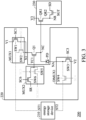
- Fig. 3 is a schematic diagram illustrating an electronic circuit operating in a sensing mode in accordance with an embodiment of the disclosure, in which the dotted line in Fig. 3 represents that the path of the switching circuit 220 remains non-conductive, and the solid line represents that the path of the switching circuit 220 operates in a sensing mode.
- the electronic circuit 200 when the processor 122 of Fig. 1 operates in the sensing mode, the electronic circuit 200 operates in a reset state, an exposure state, and a readout state in sequence, and the switching circuit 220 electrically isolates the photodiode PD from the energy storage device 210.
- the sixth selection switch SW6 of the second multiplexer MUX2 provides the reset signal SR to the first control terminal TC1 according to the sixth control signal SC6, so as to turn on the first switch Q1.
- the first selection switch SW1 of the first multiplexer MUX1 supplies the first voltage V1 to the cathode terminal NC through the first switch Q1 according to the first control signal SC1
- the third selection switch SW3 of the first demultiplexer DMUX1 supplies the second voltage V2 to the anode terminal NA according to the third control signal SC3.
- the electronic circuit 200 After the reset state, the electronic circuit 200 operates in the exposure state.
- the first switch Q1 is turned off based on the reset signal SR, the first multiplexer MUX1 stops supplying the first voltage V1 to the first node N1, and the first demultiplexer DMUX1 continuously supplies the second voltage V2 to the anode terminal NA.
- the photodiode PD when the electronic circuit 200 operates in an exposure state, the photodiode PD is configured to sense light to generate the fingerprint information. According to another embodiment of the disclosure, the photodiode PD senses the fingerprint in the exposure state.
- the electronic circuit 200 After the exposure state, the electronic circuit 200 then operates in the readout state.
- the first readout switch QR1 of the readout circuit 230 When the electronic circuit 200 operates in the readout state, the first readout switch QR1 of the readout circuit 230 generates the data signal SD based on the voltage of the cathode terminal NC, and the second read switch QR2 outputs the data signal SD according to the gate signal SGT.
- the data signal SD is configured to represent a grayscale value
- the processor 122 in Fig. 1 compares the data signal SD with the fingerprint of the user stored in the memory 121 to complete the fingerprint identification.
- Fig. 4 is a schematic diagram illustrating an electronic circuit operating in a charging mode in accordance with an embodiment of the disclosure, in which the dotted line in Fig. 4 represents that the path of the switching circuit 220 remains non-conductive, and the solid line represents that the path of the switching circuit 220 operates in the charging mode.
- the fifth selection switch SW5 of the second multiplexer MUX2 supplies the first charging signal SCHG1 to the first control terminal TC1 according to the fifth control signal SC5, so as to turn on the first switch Q1.
- the second selection switch SW2 of the first multiplexer MUX1 electrically connects the first node N1 to the first energy storage terminal ST1 of the energy storage device 210 according to the second control signal SC2.
- the fourth selection switch SW4 of the first demultiplexer DMUX1 electrically connects the second energy storage terminal ST2 of the energy storage device 210 to the anode terminal NA according to the fourth control signal SC4. Therefore, the photodiode PD charges the energy storage device 210 with the photocurrent IL generated by the light sensed. According to an embodiment of the disclosure, the voltage of the second energy storage terminal ST2 exceeds the voltage of the first energy storage terminal ST1.
- Fig. 5 is a circuit diagram illustrating an electronic circuit in accordance with another embodiment of the disclosure. Comparing the electronic circuit 500 of Fig. 5 with the electronic circuit 200 of Fig. 2 , the electronic circuit 500 further includes a second switch Q2, and the switching circuit 520 of the electronic circuit 500 further includes a third multiplexer MUX3.
- the second switch Q2 is electrically connected between the first switch Q1 and the cathode terminal NC, and includes a second control terminal TC2, in which the second switch Q2 is turned on or off according to the signal received by the second control terminal TC2.
- the first switch Q1 and the second switch Q2 are electrically connected to the second node N2, and the readout circuit 230 generates the data signal SD based on the voltage of the second node N2.
- the third multiplexer MUX3 includes a seventh selection switch SW7 and an eighth selection switch SW8.
- the seventh selection switch SW7 provides the second charging signal SCHG2 to the second control terminal TC2 according to the seventh control signal SC7
- the eighth selection switch SW8 reads the control signal SRC according to the eighth control signal SC8.
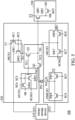
- Fig. 6 is a schematic diagram illustrating an electronic circuit operating in a sensing mode in accordance with another embodiment of the disclosure, in which the dotted line in Fig. 6 represents that the path of the switching circuit 520 remains non-conductive, and the solid line represents that the path of the switching circuit 520 operates in a sense mode.
- the electronic circuit 500 when the processor 122 of Fig. 1 operates in the sensing mode, the electronic circuit 500 operates in a reset state, an exposure state, and a readout state in sequence, and the switching circuit 520 electrically isolates the photodiode PD from the energy storage device 210.
- the sixth selection switch SW6 of the second multiplexer MUX2 provides the reset signal SR to the first control terminal TC1 according to the sixth control signal SC6, so as to turn on the first switch Q1.
- the eighth selection switch SW8 of the third multiplexer MUX3 provides the readout control signal SRC to the second control terminal TC2 according to the eighth control signal SC8, so as to turn on the second switch Q2.
- the first selection switch SW1 of the first multiplexer MUX1 supplies the first voltage V1 to the cathode terminal NC through the first switch Q1 and the second switch Q2 according to the first control signal SC1, and
- the third selection switch SW3 of the first demultiplexer DMUX1 provides the second voltage V2 to the anode terminal NA according to the third control signal SC3.
- the electronic circuit 500 After the reset state, the electronic circuit 500 operates in the exposure state.
- the first switch Q1 When the electronic circuit 500 operates in the exposure state, the first switch Q1 is turned off based on the reset signal SR, and the eighth selection switch SW8 is turned off based on the eighth control signal SC8, so that the readout control signal SRC is stopped providing to the second switch Q2, the first multiplexer MUX1 stops providing the first voltage V1 to the first node N1, and the first demultiplexer DMUX1 continuously provides the second voltage V2 to the anode terminal NA.
- the photodiode PD when the electronic circuit 500 operates in an exposure state, the photodiode PD is configured to sense light to generate the fingerprint information.
- the photodiode PD senses the fingerprint in the exposure state.
- the electronic circuit 500 After the exposure state, the electronic circuit 500 then operates in the readout state.
- the first readout switch QR1 of the readout circuit 230 When the electronic circuit 500 operates in the readout state, the first readout switch QR1 of the readout circuit 230 generates the data signal SD based on the voltage of the second node N2.
- the second readout switch QR2 outputs the data signal SD according to the gate signal SGT.
- the first readout switch QR1 of the readout circuit 230 generates the data signal SD through the second switch Q2 based on the voltage of the cathode terminal NC.
- the data signal SD is configured to represent a grayscale value, and the processor 122 in Fig. 1 compares the data signal SD with the fingerprint of the user stored in the memory 121 to complete the fingerprint identification.
- the second switch Q2 helps to reduce the leakage phenomenon of the cathode terminal NC, thereby improving the accuracy of the data signal SD generated by the readout circuit 230.
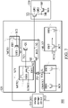
- Fig. 7 is a schematic diagram illustrating an electronic circuit operating in a charging mode according to another embodiment of the disclosure, in which the dotted line in Fig. 7 represents that the path of the switching circuit 520 remains non-conductive, and the solid line represents that the path of the switching circuit 520 operates in the charging mode.
- the electronic circuit 500 also operates in the charging mode, and the fifth selection switch SW5 of the second multiplexer MUX2 provides the first charging signal SCHG1 to the fifth control signal SC5 according to the fifth control signal SC5, so as to turn on the first switch Q1.
- the seventh selection switch SW7 of the third multiplexer MUX3 provides the second charging signal SCHG2 to the second control terminal TC2 according to the seventh control signal SC7, so as to turn on the second switch Q2.
- the second selection switch SW2 of the first multiplexer MUX1 electrically connects the first node N1 to the first energy storage terminal ST1 of the energy storage device 210 according to the second control signal SC2.
- the fourth selection switch SW4 of the first demultiplexer DMUX1 electrically connects the second energy storage terminal ST2 of the energy storage device 210 to the anode terminal NA according to the fourth control signal SC4. Therefore, the photodiode PD can charge the energy storage device 210 with the photocurrent IL generated by the light sensed.
- Fig. 8 is a circuit diagram illustrating an electronic circuit in accordance with another embodiment of the disclosure.
- the electronic circuit 800 includes an energy storage device 210, a photodiode PD, a first switch Q1, and a switching circuit 820, in which the energy storage device 210 corresponds to the energy storage device 110 in Fig. 1 .
- the switching circuit 820 is located in the electronic device.
- the switching circuit 820 is electrically connected between the energy storage device 210 and the photodiode PD, and the switching circuit 820 includes a fourth multiplexer MUX4 and a second demultiplexer DMUX2.
- the first switch Q1 electrically connects the first node N1 to the cathode terminal NC according to the gate signal SGT.
- the fourth multiplexer MUX4 includes a ninth selection switch SW9 and a tenth selection switch SW10.
- the ninth selection switch SW9 electrically connects the first external node NEX1 to the first node N1 according to the ninth control signal SC9.
- the tenth selection switch SW10 electrically connects the first energy storage terminal ST1 of the energy storage device 210 to the first node N1 according to the tenth control signal SC10.
- the second demultiplexer DMUX2 includes an eleventh selection switch SW11 and a twelfth selection switch SW12.
- the eleventh selection switch SW11 electrically connects the second external node NEX2 to the anode terminal NA according to the eleventh control signal SC11.
- the twelfth selection switch SW12 electrically connects the second energy storage terminal ST2 of the energy storage device 210 to the anode terminal NA according to the twelfth control signal SC12.
- the switching circuit 820 when the processor 122 of Fig. 1 operates in the sensing mode, the switching circuit 820 electrically isolates the photodiode PD from the energy storage device 210, and the first external The node NEX1 outputs an output signal SD.
- the switching circuit 820 when the processor 122 in Fig. 1 operates in the charging mode, the switching circuit 820 electrically connects the photodiode PD to the energy storage device 210, so that the photodiode PD can charge the energy storage device 210 with the photocurrent IL converted from the light.
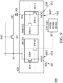
- Fig. 9 is a schematic diagram illustrating an electronic circuit operating in a sensing mode in accordance with an embodiment of the disclosure, in which the dotted line in Fig. 9 represents the path of the switching circuit 820 and remains non-conductive, and the solid line represents that the path of the switching circuit 820 operates in the sensing mode.
- the electronic circuit 800 when the processor 122 of Fig. 1 operates in the sensing mode, the electronic circuit 800 operates in the reset state RST, the exposure state EXP, and the readout state RD in sequence, and the switching circuit 820 electrically isolates the light The sense diode PD and the energy storage device 210 from each other.
- the first switch Q1 When the electronic circuit 800 operates in the reset state RST, the first switch Q1 is turned on according to the gate signal SGT, and the ninth selection switch SW9 of the fourth multiplexer MUX4 electrically connects the first external node NEX1 to the first node N1 according to the ninth control signal SC9.
- the eleventh selection switch SW11 of the second demultiplexer DMUX2 electrically connects the second external node NEX2 to the anode terminal NA according to the eleventh control signal SC11.
- the first external node NEX1 receives the first external voltage VE1
- the second external node NEX2 receives the second external voltage VE2.
- the second external voltage VE2 exceeds the first external voltage VE1. Since the voltage of the anode terminal NA exceeds the voltage of the cathode terminal NC, the photodiode PD is forward biased, and the voltage difference between the anode terminal NA and the first node N1 is (VE1-VE2).
- the electronic circuit 800 After the reset state RST, the electronic circuit 800 operates in the exposure state EXP.
- the first switch Q1 is turned off according to the gate signal SGT, and the second external node NEX2 receives the third external voltage VE3.
- the third external voltage VE3 is smaller than the second external voltage VE2.
- the photodiode PD is reverse biased.
- the photodiode PD when the electronic circuit 800 operates in the exposure state EXP, the photodiode PD is configured to sense the light to generate the fingerprint information.
- the photodiode PD performs the fingerprint sensing in the exposure state EXP.
- the electronic circuit 800 After the exposure state EXP, the electronic circuit 800 then operates in the readout state RD.
- the first switch Q1 is turned on according to the gate signal SGT, and the voltage of the cathode terminal NC is passed through the first switch Q1 and the fourth multiplexer MUX4 to generate the data signal SD at the first external node NEX1.
- the data signal SD is a DC voltage, in which the DC voltage value of the data signal SD is configured to represent a grayscale value, and the processor 122 in Fig. 1 compares the data signal SD with the user's fingerprints stored in the memory 121 to complete the fingerprint identification.
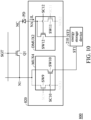
- Fig. 10 is a schematic diagram illustrating an electronic circuit operating in a charging mode in accordance with another embodiment of the disclosure, in which the dotted line in Fig. 10 represents that the path of the switching circuit 820 remains non-conductive, and the solid line represents that the path of the switching circuit 820 operates in the charging mode.
- the first switch Q1 is turned on according to the gate signal SGT
- the fourth multiplexer MUX4 electrically connects the first node N1 to the first energy storage terminal ST1 of the energy storage device 210
- the second demultiplexer DMUX2 electrically connects the second energy storage terminal ST2 of the energy storage device 210 to the anode terminal NA. Therefore, the photodiode PD charges the energy storage device 210 with the photocurrent IL generated by the light sensed.
- the voltage of the second energy storage terminal ST2 exceeds the voltage of the first energy storage terminal ST1.
- the disclosure proposes an electronic device with a photodiode having an optical sensing function and a solar charging function that are switchable, so that the photodiode can charge the energy storage device in addition to fingerprint recognition, thereby effectively prolonging the use time of the electronic device or improving the convenience of charging the electronic device.
Landscapes
- Engineering & Computer Science (AREA)
- General Physics & Mathematics (AREA)
- Physics & Mathematics (AREA)
- Power Engineering (AREA)
- Human Computer Interaction (AREA)
- Multimedia (AREA)
- Theoretical Computer Science (AREA)
- Spectroscopy & Molecular Physics (AREA)
- Computer Networks & Wireless Communication (AREA)
- Photometry And Measurement Of Optical Pulse Characteristics (AREA)
- Electronic Switches (AREA)
- Transforming Light Signals Into Electric Signals (AREA)
- Surgical Instruments (AREA)
- Valve Device For Special Equipments (AREA)
- Noodles (AREA)
Applications Claiming Priority (1)
| Application Number | Priority Date | Filing Date | Title |
|---|---|---|---|
| CN202111127687.1A CN115877931A (zh) | 2021-09-26 | 2021-09-26 | 电子装置 |
Publications (1)
| Publication Number | Publication Date |
|---|---|
| EP4156514A1 true EP4156514A1 (de) | 2023-03-29 |
Family
ID=83318855
Family Applications (1)
| Application Number | Title | Priority Date | Filing Date |
|---|---|---|---|
| EP22191784.2A Withdrawn EP4156514A1 (de) | 2021-09-26 | 2022-08-23 | Elektronische vorrichtung mit einer photodiode und der fähigkeit zum umschalten zwischen lichterfassungsfunktion und lichtladefunktion |
Country Status (4)
| Country | Link |
|---|---|
| US (1) | US11976967B2 (de) |
| EP (1) | EP4156514A1 (de) |
| CN (1) | CN115877931A (de) |
| TW (1) | TWI824540B (de) |
Families Citing this family (1)
| Publication number | Priority date | Publication date | Assignee | Title |
|---|---|---|---|---|
| CN116418088B (zh) * | 2023-04-17 | 2024-03-12 | 基康仪器股份有限公司 | 一种应用于光纤的电路及装置 |
Citations (4)
| Publication number | Priority date | Publication date | Assignee | Title |
|---|---|---|---|---|
| EP0064025A1 (de) * | 1981-04-22 | 1982-11-03 | Asulab S.A. | Elektronische Uhr mit unbewegbarer Steuervorrichtung |
| KR20200025078A (ko) * | 2018-08-29 | 2020-03-10 | 엘지디스플레이 주식회사 | 광전지가 내장된 표시 장치 |
| US20210124896A1 (en) * | 2019-05-27 | 2021-04-29 | Boe Technology Group Co., Ltd. | Texture detection circuit, charging circuit, driving method and touch display panel |
| US20210210964A1 (en) * | 2019-03-08 | 2021-07-08 | Boe Technology Group Co., Ltd. | Photoelectric conversion circuit, driving method thereof, photosensitive device and display device |
Family Cites Families (10)
| Publication number | Priority date | Publication date | Assignee | Title |
|---|---|---|---|---|
| GB9614480D0 (en) * | 1995-12-01 | 1996-09-04 | Philips Electronics Nv | Multiplexer circuit |
| TW201240263A (en) * | 2011-03-28 | 2012-10-01 | Kye Systems Corp | Wireless electronic apparatus |
| CN102904982A (zh) * | 2011-07-29 | 2013-01-30 | 富泰华工业(深圳)有限公司 | 电子配件 |
| TWI534630B (zh) * | 2015-10-23 | 2016-05-21 | 國立勤益科技大學 | 傳輸系統以及相關的傳輸方法 |
| JP7222656B2 (ja) * | 2018-10-24 | 2023-02-15 | 株式会社ジャパンディスプレイ | 指紋検出装置及び指紋検出装置付き表示装置 |
| KR102761617B1 (ko) * | 2018-12-26 | 2025-02-03 | 애플 인크. | 광학 지문 검출 시스템 |
| CN109950235B (zh) | 2019-03-13 | 2020-10-27 | 武汉华星光电半导体显示技术有限公司 | 一种集成指纹识别功能及太阳能电池模块的显示装置 |
| CN118887709A (zh) * | 2019-06-28 | 2024-11-01 | 群创光电股份有限公司 | 电子装置 |
| TWI851794B (zh) * | 2019-08-22 | 2024-08-11 | 美商光程研創股份有限公司 | 光電流放大裝置及光電偵測裝置之操作方法 |
| TWI738422B (zh) * | 2020-07-16 | 2021-09-01 | 友達光電股份有限公司 | 用於觸控感測與光感測的畫素電路 |
-
2021
- 2021-09-26 CN CN202111127687.1A patent/CN115877931A/zh active Pending
-
2022
- 2022-05-27 TW TW111119855A patent/TWI824540B/zh active
- 2022-08-19 US US17/820,963 patent/US11976967B2/en active Active
- 2022-08-23 EP EP22191784.2A patent/EP4156514A1/de not_active Withdrawn
Patent Citations (4)
| Publication number | Priority date | Publication date | Assignee | Title |
|---|---|---|---|---|
| EP0064025A1 (de) * | 1981-04-22 | 1982-11-03 | Asulab S.A. | Elektronische Uhr mit unbewegbarer Steuervorrichtung |
| KR20200025078A (ko) * | 2018-08-29 | 2020-03-10 | 엘지디스플레이 주식회사 | 광전지가 내장된 표시 장치 |
| US20210210964A1 (en) * | 2019-03-08 | 2021-07-08 | Boe Technology Group Co., Ltd. | Photoelectric conversion circuit, driving method thereof, photosensitive device and display device |
| US20210124896A1 (en) * | 2019-05-27 | 2021-04-29 | Boe Technology Group Co., Ltd. | Texture detection circuit, charging circuit, driving method and touch display panel |
Also Published As
| Publication number | Publication date |
|---|---|
| TW202314462A (zh) | 2023-04-01 |
| US20230094256A1 (en) | 2023-03-30 |
| US11976967B2 (en) | 2024-05-07 |
| TWI824540B (zh) | 2023-12-01 |
| CN115877931A (zh) | 2023-03-31 |
Similar Documents
| Publication | Publication Date | Title |
|---|---|---|
| EP3605293B1 (de) | Anzeigevorrichtung | |
| US8482263B2 (en) | Rapid transfer of stored energy | |
| US20100327802A1 (en) | Charging device and charging system having same | |
| US20080258678A1 (en) | Mobile type power supply, connection device, and carried type electronic equipment | |
| US8258808B2 (en) | System for testing power supply performance | |
| US11393245B2 (en) | Texture detection circuit, charging circuit, driving method and touch display panel | |
| CN101349821A (zh) | 用以得知光线强度的读取电路及电子系统 | |
| US8866806B2 (en) | Method and apparatus for supplying power to an electronic device using a solar battery | |
| US11646577B2 (en) | Electronic device and control method | |
| US11976967B2 (en) | Electronic device having a photodiode and capable of switching between light-sensing function and light-charging function | |
| CN100380278C (zh) | 电器 | |
| US8723485B2 (en) | Power supply system | |
| EP3739739A1 (de) | Leistungsumwandlungsvorrichtung und -verfahren | |
| WO2019109896A1 (en) | Photodetection apparatus | |
| TWI345172B (en) | Systems for displaying and capturing images | |
| US20230238823A1 (en) | Electronic Apparatus, Display Panel, and Electronic Device | |
| KR20140130806A (ko) | 태양전지를 이용한 휴대용 충전장치 | |
| CN111781758A (zh) | 显示屏及电子设备 | |
| US8963400B2 (en) | Piezo driver having recharging capability | |
| CN118111557A (zh) | 光电传感电路及显示装置 | |
| KR20230047626A (ko) | 전자 장치 및 이의 동작 방법 | |
| CN221040068U (zh) | 指纹识别装置、指纹模组及电子设备 | |
| CN114724483B (zh) | 一种光电转换电路及其驱动方法、显示装置 | |
| CN221040067U (zh) | 驱动模块、封装芯片、指纹识别装置、模组及电子设备 | |
| KR20210050023A (ko) | 전자 장치 |
Legal Events
| Date | Code | Title | Description |
|---|---|---|---|
| PUAI | Public reference made under article 153(3) epc to a published international application that has entered the european phase |
Free format text: ORIGINAL CODE: 0009012 |
|
| STAA | Information on the status of an ep patent application or granted ep patent |
Free format text: STATUS: THE APPLICATION HAS BEEN PUBLISHED |
|
| AK | Designated contracting states |
Kind code of ref document: A1 Designated state(s): AL AT BE BG CH CY CZ DE DK EE ES FI FR GB GR HR HU IE IS IT LI LT LU LV MC MK MT NL NO PL PT RO RS SE SI SK SM TR |
|
| STAA | Information on the status of an ep patent application or granted ep patent |
Free format text: STATUS: THE APPLICATION IS DEEMED TO BE WITHDRAWN |
|
| 18D | Application deemed to be withdrawn |
Effective date: 20230930 |