EP4160302B1 - Module d'affichage, son procédé de commande, appareil d'affichage et véhicule - Google Patents
Module d'affichage, son procédé de commande, appareil d'affichage et véhicule Download PDFInfo
- Publication number
- EP4160302B1 EP4160302B1 EP22175455.9A EP22175455A EP4160302B1 EP 4160302 B1 EP4160302 B1 EP 4160302B1 EP 22175455 A EP22175455 A EP 22175455A EP 4160302 B1 EP4160302 B1 EP 4160302B1
- Authority
- EP
- European Patent Office
- Prior art keywords
- electrode
- light
- liquid crystal
- display module
- component
- Prior art date
- Legal status (The legal status is an assumption and is not a legal conclusion. Google has not performed a legal analysis and makes no representation as to the accuracy of the status listed.)
- Active
Links
Images















Classifications
-
- G—PHYSICS
- G02—OPTICS
- G02F—OPTICAL DEVICES OR ARRANGEMENTS FOR THE CONTROL OF LIGHT BY MODIFICATION OF THE OPTICAL PROPERTIES OF THE MEDIA OF THE ELEMENTS INVOLVED THEREIN; NON-LINEAR OPTICS; FREQUENCY-CHANGING OF LIGHT; OPTICAL LOGIC ELEMENTS; OPTICAL ANALOGUE/DIGITAL CONVERTERS
- G02F1/00—Devices or arrangements for the control of the intensity, colour, phase, polarisation or direction of light arriving from an independent light source, e.g. switching, gating or modulating; Non-linear optics
- G02F1/01—Devices or arrangements for the control of the intensity, colour, phase, polarisation or direction of light arriving from an independent light source, e.g. switching, gating or modulating; Non-linear optics for the control of the intensity, phase, polarisation or colour
- G02F1/13—Devices or arrangements for the control of the intensity, colour, phase, polarisation or direction of light arriving from an independent light source, e.g. switching, gating or modulating; Non-linear optics for the control of the intensity, phase, polarisation or colour based on liquid crystals, e.g. single liquid crystal display cells
- G02F1/1323—Arrangements for providing a switchable viewing angle
-
- G—PHYSICS
- G02—OPTICS
- G02F—OPTICAL DEVICES OR ARRANGEMENTS FOR THE CONTROL OF LIGHT BY MODIFICATION OF THE OPTICAL PROPERTIES OF THE MEDIA OF THE ELEMENTS INVOLVED THEREIN; NON-LINEAR OPTICS; FREQUENCY-CHANGING OF LIGHT; OPTICAL LOGIC ELEMENTS; OPTICAL ANALOGUE/DIGITAL CONVERTERS
- G02F1/00—Devices or arrangements for the control of the intensity, colour, phase, polarisation or direction of light arriving from an independent light source, e.g. switching, gating or modulating; Non-linear optics
- G02F1/01—Devices or arrangements for the control of the intensity, colour, phase, polarisation or direction of light arriving from an independent light source, e.g. switching, gating or modulating; Non-linear optics for the control of the intensity, phase, polarisation or colour
- G02F1/13—Devices or arrangements for the control of the intensity, colour, phase, polarisation or direction of light arriving from an independent light source, e.g. switching, gating or modulating; Non-linear optics for the control of the intensity, phase, polarisation or colour based on liquid crystals, e.g. single liquid crystal display cells
- G02F1/133—Constructional arrangements; Operation of liquid crystal cells; Circuit arrangements
- G02F1/1333—Constructional arrangements; Manufacturing methods
- G02F1/1335—Structural association of cells with optical devices, e.g. polarisers or reflectors
- G02F1/133528—Polarisers
- G02F1/133531—Polarisers characterised by the arrangement of polariser or analyser axes
-
- G—PHYSICS
- G02—OPTICS
- G02F—OPTICAL DEVICES OR ARRANGEMENTS FOR THE CONTROL OF LIGHT BY MODIFICATION OF THE OPTICAL PROPERTIES OF THE MEDIA OF THE ELEMENTS INVOLVED THEREIN; NON-LINEAR OPTICS; FREQUENCY-CHANGING OF LIGHT; OPTICAL LOGIC ELEMENTS; OPTICAL ANALOGUE/DIGITAL CONVERTERS
- G02F1/00—Devices or arrangements for the control of the intensity, colour, phase, polarisation or direction of light arriving from an independent light source, e.g. switching, gating or modulating; Non-linear optics
- G02F1/01—Devices or arrangements for the control of the intensity, colour, phase, polarisation or direction of light arriving from an independent light source, e.g. switching, gating or modulating; Non-linear optics for the control of the intensity, phase, polarisation or colour
- G02F1/13—Devices or arrangements for the control of the intensity, colour, phase, polarisation or direction of light arriving from an independent light source, e.g. switching, gating or modulating; Non-linear optics for the control of the intensity, phase, polarisation or colour based on liquid crystals, e.g. single liquid crystal display cells
- G02F1/133—Constructional arrangements; Operation of liquid crystal cells; Circuit arrangements
- G02F1/1333—Constructional arrangements; Manufacturing methods
- G02F1/1335—Structural association of cells with optical devices, e.g. polarisers or reflectors
- G02F1/1336—Illuminating devices
- G02F1/133602—Direct backlight
- G02F1/133606—Direct backlight including a specially adapted diffusing, scattering or light controlling members
-
- G—PHYSICS
- G02—OPTICS
- G02F—OPTICAL DEVICES OR ARRANGEMENTS FOR THE CONTROL OF LIGHT BY MODIFICATION OF THE OPTICAL PROPERTIES OF THE MEDIA OF THE ELEMENTS INVOLVED THEREIN; NON-LINEAR OPTICS; FREQUENCY-CHANGING OF LIGHT; OPTICAL LOGIC ELEMENTS; OPTICAL ANALOGUE/DIGITAL CONVERTERS
- G02F1/00—Devices or arrangements for the control of the intensity, colour, phase, polarisation or direction of light arriving from an independent light source, e.g. switching, gating or modulating; Non-linear optics
- G02F1/01—Devices or arrangements for the control of the intensity, colour, phase, polarisation or direction of light arriving from an independent light source, e.g. switching, gating or modulating; Non-linear optics for the control of the intensity, phase, polarisation or colour
- G02F1/13—Devices or arrangements for the control of the intensity, colour, phase, polarisation or direction of light arriving from an independent light source, e.g. switching, gating or modulating; Non-linear optics for the control of the intensity, phase, polarisation or colour based on liquid crystals, e.g. single liquid crystal display cells
- G02F1/133—Constructional arrangements; Operation of liquid crystal cells; Circuit arrangements
- G02F1/1333—Constructional arrangements; Manufacturing methods
- G02F1/1337—Surface-induced orientation of the liquid crystal molecules, e.g. by alignment layers
-
- G—PHYSICS
- G02—OPTICS
- G02F—OPTICAL DEVICES OR ARRANGEMENTS FOR THE CONTROL OF LIGHT BY MODIFICATION OF THE OPTICAL PROPERTIES OF THE MEDIA OF THE ELEMENTS INVOLVED THEREIN; NON-LINEAR OPTICS; FREQUENCY-CHANGING OF LIGHT; OPTICAL LOGIC ELEMENTS; OPTICAL ANALOGUE/DIGITAL CONVERTERS
- G02F1/00—Devices or arrangements for the control of the intensity, colour, phase, polarisation or direction of light arriving from an independent light source, e.g. switching, gating or modulating; Non-linear optics
- G02F1/01—Devices or arrangements for the control of the intensity, colour, phase, polarisation or direction of light arriving from an independent light source, e.g. switching, gating or modulating; Non-linear optics for the control of the intensity, phase, polarisation or colour
- G02F1/13—Devices or arrangements for the control of the intensity, colour, phase, polarisation or direction of light arriving from an independent light source, e.g. switching, gating or modulating; Non-linear optics for the control of the intensity, phase, polarisation or colour based on liquid crystals, e.g. single liquid crystal display cells
- G02F1/133—Constructional arrangements; Operation of liquid crystal cells; Circuit arrangements
- G02F1/1333—Constructional arrangements; Manufacturing methods
- G02F1/1343—Electrodes
- G02F1/13439—Electrodes characterised by their electrical, optical, physical properties; materials therefor; method of making
-
- G—PHYSICS
- G02—OPTICS
- G02F—OPTICAL DEVICES OR ARRANGEMENTS FOR THE CONTROL OF LIGHT BY MODIFICATION OF THE OPTICAL PROPERTIES OF THE MEDIA OF THE ELEMENTS INVOLVED THEREIN; NON-LINEAR OPTICS; FREQUENCY-CHANGING OF LIGHT; OPTICAL LOGIC ELEMENTS; OPTICAL ANALOGUE/DIGITAL CONVERTERS
- G02F1/00—Devices or arrangements for the control of the intensity, colour, phase, polarisation or direction of light arriving from an independent light source, e.g. switching, gating or modulating; Non-linear optics
- G02F1/01—Devices or arrangements for the control of the intensity, colour, phase, polarisation or direction of light arriving from an independent light source, e.g. switching, gating or modulating; Non-linear optics for the control of the intensity, phase, polarisation or colour
- G02F1/13—Devices or arrangements for the control of the intensity, colour, phase, polarisation or direction of light arriving from an independent light source, e.g. switching, gating or modulating; Non-linear optics for the control of the intensity, phase, polarisation or colour based on liquid crystals, e.g. single liquid crystal display cells
- G02F1/133—Constructional arrangements; Operation of liquid crystal cells; Circuit arrangements
- G02F1/1333—Constructional arrangements; Manufacturing methods
- G02F1/1337—Surface-induced orientation of the liquid crystal molecules, e.g. by alignment layers
- G02F1/133738—Surface-induced orientation of the liquid crystal molecules, e.g. by alignment layers for homogeneous alignment
-
- G—PHYSICS
- G02—OPTICS
- G02F—OPTICAL DEVICES OR ARRANGEMENTS FOR THE CONTROL OF LIGHT BY MODIFICATION OF THE OPTICAL PROPERTIES OF THE MEDIA OF THE ELEMENTS INVOLVED THEREIN; NON-LINEAR OPTICS; FREQUENCY-CHANGING OF LIGHT; OPTICAL LOGIC ELEMENTS; OPTICAL ANALOGUE/DIGITAL CONVERTERS
- G02F1/00—Devices or arrangements for the control of the intensity, colour, phase, polarisation or direction of light arriving from an independent light source, e.g. switching, gating or modulating; Non-linear optics
- G02F1/01—Devices or arrangements for the control of the intensity, colour, phase, polarisation or direction of light arriving from an independent light source, e.g. switching, gating or modulating; Non-linear optics for the control of the intensity, phase, polarisation or colour
- G02F1/13—Devices or arrangements for the control of the intensity, colour, phase, polarisation or direction of light arriving from an independent light source, e.g. switching, gating or modulating; Non-linear optics for the control of the intensity, phase, polarisation or colour based on liquid crystals, e.g. single liquid crystal display cells
- G02F1/133—Constructional arrangements; Operation of liquid crystal cells; Circuit arrangements
- G02F1/1333—Constructional arrangements; Manufacturing methods
- G02F1/1337—Surface-induced orientation of the liquid crystal molecules, e.g. by alignment layers
- G02F1/133742—Surface-induced orientation of the liquid crystal molecules, e.g. by alignment layers for homeotropic alignment
Definitions
- the present disclosure relates to the field of display technologies, and, particularly, relates to a display module, a method for driving the display module, a display apparatus, and a vehicle.
- a viewing angle of a display panel has been expanded to more than 160°.
- it is liable to cause the leakage of personal privacy while enjoying the visual experience brought by the large viewing angle.
- a user uses a display apparatus in public to access bank accounts, pay bills, or enter personal information, there is a risk of identity theft and privacy violations.
- JP4968656B2 discloses a light source device with which the illuminating angle range of light is made variable and of which the efficiency of utilizing light is high, a liquid crystal display device, and a personal digital assistant.
- the light source device includes a reflective polarizing element which transmits only specified polarized light and reflects polarized light with a property opposite to that of the specified polarized light, a light beam direction controlling element which is composed of a transparent region and a light shielding region and restricts spreading of light emitted from a backlight, a transparent and scattering switching element which scatters light when no voltage is applied thereto and transmits light when voltage is applied thereto, and a liquid crystal panel are disposed on the light emitting surface side of a light guide plate of the backlight in this order.
- US2020326567A1 discloses a viewing angle switch module including a viewing angle limiting device and a first electrically controlled viewing angle switch device.
- a plurality of first block walls of the viewing angle limiting device are arranged along a first direction and extended in a second direction.
- the first electrically controlled viewing angle switch device has a first liquid crystal layer, a first polarizer and a second polarizer.
- An angle of 90 ⁇ 20 degrees is included between an optical axis of the first liquid crystal layer and the first direction.
- the first polarizer and the second polarizer are respectively located at two opposite sides of the first liquid crystal layer.
- An absorption axis of the first polarizer and a, absorption axis of the second polarizer are parallel to or perpendicular to the first direction.
- US2021271132A1 discloses a display apparatus that includes a backlight source, a privacy filter disposed on the backlight source, a light adjusting panel disposed on the privacy filter, and a display panel disposed on the light adjusting panel.
- the light adjusting panel includes a first substrate, a first electrode, a second electrode, a first vertical alignment film disposed on the first substrate, a second substrate disposed opposite to the first substrate, a second vertical alignment film disposed on the second substrate, and a positive liquid crystal layer disposed between the first vertical alignment film and the second vertical alignment film.
- the first electrode and the second electrode are disposed on the first substrate.
- US2021055582A1 discloses a viewing angle control device that includes a plurality of first polarizing portions and a plurality of transmissive portions.
- the first polarizing portions are arranged along a first direction and extended in a second direction.
- the transmissive portions and the first polarizing portions are alternately arranged.
- Each of the first polarizing portions has a width in the first direction and a height in a direction perpendicular to the first direction and the second direction. A ratio of the height to the width of the first polarizing portion is greater than 1.
- CN212255969U discloses a display device.
- the viewing angle is wide, liquid crystal molecules in the first liquid crystal layer are in a lying posture, no electric signal is applied to the first electrode and the second electrode, or a small voltage is applied to the first electrode and the second electrode, so that the polymer dispersed liquid crystal layer is in a mist state and has a lightscattering effect;
- the viewing angle is narrow, liquid crystal molecules in the first liquid crystal layer are in an inclined posture, corresponding electric signals are applied to the first electrode and the second electrode respectively, a large electric field is formed between the first electrode and the second electrode, and the polymer dispersed liquid crystal layer is in a transparent state.
- a display module in a first aspect of the present invention, includes a backlight component, a display component located on a side of the backlight component facing toward a light-emitting direction of the display module, and a light-adjusting component located on the side of the backlight component facing toward the light-emitting direction of the display module.
- the backlight component comprises a first light guide structure and a light regulating structure
- the first light guide structure comprises a first light source and a first light guide plate
- the light regulating structure is located on a side of the first light guide plate facing toward the display component and is configured to regulate a transmission direction of light emitted from the first light guide plate.
- the light-adjusting component comprises a first electrode, a first liquid crystal located on a side of the first electrode facing away from the backlight component, and a second electrode located at a side of the first liquid crystal facing away from the backlight component; and the light-adjusting component and the light regulating structure are configured to regulate light to a same direction.
- the display module has a sharing mode and an anti-peeping mode, wherein in the sharing mode, the first electrode and the second electrode are not energized, and the first liquid crystal is in a wide viewing angle state; and in the anti-peeping mode, the first electrode and the second electrode drive the first liquid crystals to be in a narrow viewing angle state.
- the backlight component further includes a second light guide structure, the second light guide structure includes a second light source and a second light guide plate located at a side of the light regulating structure facing away from the first light guide plate, and the second light source is turned on in the sharing mode, and the second light source is turned off in the anti-peeping mode.
- the angle formed between the optical axis P of the first liquid crystal 9 and the plane of the display module is close to 45°, the influence of the first liquid crystal 9 on the optical characteristics of the second linear polarizing light W2 under the oblique viewing angle tends to be the greatest, and the polarization state of the second polarizing light W2 after passing through the first liquid crystal 9 has been changed to a greater extent, so that more second polarizing light cannot be emitted through the third polarizer 23, thereby increasing the luminance attenuation under the oblique viewing angle and improving the anti-peeping effect.
- a cell gap d1 of the first liquid crystal 9 satisfies 5 ⁇ m ⁇ d1 ⁇ 8 ⁇ m.
- V 5.095-1.479 ⁇ ((1n( ⁇ )-1n(d1)+1)), where V denotes a voltage difference between the first electrode 8 and the second electrode 10, ⁇ denotes a difference between a dielectric constant ⁇ // and a dielectric constant ⁇ , a dielectric constant ⁇ // denotes a horizontal dielectric constant, and a dielectric constant ⁇ denotes a vertical dielectric constant, and d1 denotes a cell gap of the first liquid crystal 9 in a direction perpendicular to a plane of the display module.
- the first electrode 8 includes at least one first sub-electrode 29.
- the first sub-electrode 29 includes a first main electrode strip 30 and a plurality of first toothed electrode strips 31.
- the first toothed electrode strips 31 are connected to the first main electrode strip 30 and parallel to each other.
- the second electrode 10 covers the first liquid crystal 9 in a direction perpendicular to a plane of the display module while the second electrode 10 and the first electrode 8 are a planar electrode and a grid electrode, respectively.
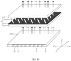
- FIG. 28 is a schematic diagram of a light-adjusting component 3
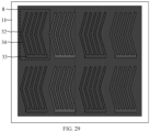
- FIG. 29 is a top view of the first electrode 8 and the second electrode 10 corresponding to FIG. 28 .
- the first electrode 8 covers the first liquid crystal 9.
- the second electrode 10 includes at least one second sub-electrode 32.
- the second sub-electrode 32 includes a second main electrode strip 33 and a plurality of second toothed electrode strips 34.
- the second toothed electrode strips 34 are connected to the second main electrode strip 33 and parallel to each other while the first electrode 8 and the second electrode 10 are a planar electrode and a grid electrode, respectively.
- one of the first electrode 8 and the second electrode 10 is a planar electrode
- the other of the first electrode 8 and the second electrode 10 is a grid electrode, as shown in FIG. 30, FIG.
- FIG. 30 is a schematic diagram showing rotation of a first liquid crystal 9 when the first electrode 8 and the second electrode 10 corresponding to FIG. 28 are energized according to an embodiment of the present invention
- a relatively uniform vertical electric field can be formed after the first electrode 8 and the second electrode 10 are energized, the first liquid crystal 9 is rotated under the action of the vertical electric field, so that the optical property of the second polarization light W2 under the oblique viewing angle is adjusted.
- one of the first electrode 8 and the second electrode 10 as a grid electrode, there is a gap between the toothed electrode strips of grid electrode, so that the degree of light shielding is small, thereby improving the light emission rate of the display module.
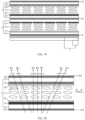
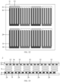
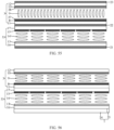
- FIG. 31 is a schematic diagram of a light-adjusting component 3
- FIG. 32 is a top view of the first electrode 8 and the second electrode 10 corresponding to FIG. 31
- the first electrode 8 includes at least one first sub-electrode 29.
- the first sub-electrode 29 includes a first main electrode strip 30 and a plurality of first toothed electrode strips 31 that is connected to the first main electrode strip 30 and parallel to each other.
- the second electrode 10 includes at least one second sub-electrode 32.
- the second sub-electrode 32 includes a second main electrode strip 33 and a plurality of second toothed electrode strips 34 that is connected to the second main electrode strip 33 and parallel to each other. Referring to FIG. 31 and FIG.
- the first electrode 8 at least partially overlaps with the second electrode 10 in a direction perpendicular to a plane of the display module.
- the first electrode 8 and the second electrode 10 each are a grid electrode.
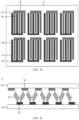
- FIG. 33 is a schematic diagram of a light-adjusting component 3
- FIG. 34 is a top view of the first electrode 8 and the second electrode 10 corresponding to FIG. 33
- FIG. 35 is a schematic diagram showing rotation of a first liquid crystal 9 when the first electrode 9 and the second electrode 10 corresponding to FIG. 33 are energized according to an embodiment of the present invention.
- the plurality of toothed electrode strips 31 of the first electrode 8 is engaged with the plurality of second toothed electrode strips 34 of the second electrode 10, so that the toothed electrode strips of the first electrode 8 are staggered with the toothed electrode strips of the second electrode 10, thereby improving the light emission rate of the display module.
- the first toothed electrode strip 31 and the second toothed electrode strip 34 have an extending direction of 90° or 270°, so that the formed electric field and the anti-peeping direction are matched with each other, thereby achieving anti-peeping at left and right viewing angles.
- the alignment direction of the alignment film can be 0° or 180°
- the extending direction of the first toothed electrode strip 31 and the second toothed electrode strip 34 can be 0° or 180°, thereby achieving the better anti-peeping at upper and lower viewing angles.
- the first electrode 8 and the second electrode 10 each are a transparent electrode.
- the first electrode 8 and the second electrode 10 are respectively formed of a light-transmitting conductive material such as indium tin oxide (ITO).
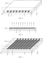
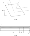
- FIG. 36 is a schematic diagram of a light regulating structure 5.
- the light regulating structure 5 includes a grating 35.
- the grating 35 includes transparent portions 70 and non-transparent portions 71 that are alternately arranged, an angle C formed between the non-transparent portion 71 and the normal line satisfies 5° ⁇ C ⁇ 10°, and the normal line is perpendicular to a plane of the display module.
- the grating 35 can use the transparent portion 70 and non-transparent portion 71 to adjust the transmission angle of the light emitted from the first light guide plate 7, and convert at least part of light into collimating light transmitted in a specific direction.
- the non-transparent portion 71 is deviated from the normal direction by 5° to 10°. After the grating 35 corrects the transmission direction of the light emitted from the first light guide plate 7, at least part of light is also transmitted in a direction oblique to the normal direction.
- the light regulating structure 5 can also be a structure such as a light control film that can adjust the transmission direction of light.
- the light control film is provided with a microstructure.
- the microstructure is configured to regulate the transmission direction of light.
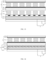
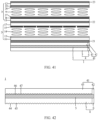
- FIG. 37 is a schematic diagram of a backlight component.
- the polymer liquid crystal film 37 includes a polymer and liquid crystal droplets uniformly dispersed in the polymer.
- the electrode layer 38 is not energized, so that the liquid crystal droplets are arranged irregularly.
- the refractive index of the liquid crystal droplets does not match with the refractive index of the polymer, and the polymer liquid crystal film 37 is in a foggy state, so that the range of the light transmission angle is increased, thereby achieving a larger viewing angle.
- the luminous power of the first light source 6 can be increased to increase the final luminance of the backlight component 1.
- the backlight component 1 further includes a first flexible circuit board.
- the pins of the first flexible circuit board are bound to the electrode layer 38.
- the first flexible circuit board is configured to transmit a voltage signal to the electrode layer 38.
- the voltage signal is used to drive the rotation of the liquid crystal droplets to rotate.
- the backlight component 1 includes a second flexible circuit board.
- the pins of the second flexible circuit board are bound to the power lead-out line or power lead-out terminal of the first light source 6.
- the second flexible circuit board is configured to transmit a power signal to the first light source 6 to control the first light source 6 to turn on.
- the first electrode 8 includes at least one first sub-electrode 29.
- the first sub-electrode 29 includes a first main electrode strip 30 and multiple first toothed electrode strips 31 connected to the bars 30 and parallel to each other.
- the second electrode 10 includes at least one second sub-electrode 32.
- the second sub-electrode 32 includes a second main electrode strip 33 and multiple second toothed electrode strips 34 connected to the second main electrode strip 33 and parallel to each other.
- the first electrode 8 at least partially overlaps with the second electrode 10 in a direction perpendicular to a plane of the first polarizer 21.
- the first electrode 8 and the second electrode 10 each are a grid electrode.
Landscapes
- Physics & Mathematics (AREA)
- Nonlinear Science (AREA)
- Chemical & Material Sciences (AREA)
- Crystallography & Structural Chemistry (AREA)
- General Physics & Mathematics (AREA)
- Optics & Photonics (AREA)
- Mathematical Physics (AREA)
- Spectroscopy & Molecular Physics (AREA)
- Liquid Crystal (AREA)
- Liquid Crystal Display Device Control (AREA)
Claims (19)
- Module d'affichage, comprenant :un composant de rétroéclairage (1) ;un composant d'affichage (2) situé sur un côté du composant de rétroéclairage (1) orienté vers une direction d'émission de lumière du module d'affichage ; etun composant de réglage de lumière (3) situé sur le côté du composant de rétroéclairage (1) orienté vers la direction d'émission de lumière du module d'affichage ;le composant de rétroéclairage (1) comprenant une première structure de guidage de lumière (4) et une structure de régulation de lumière (5), la première structure de guidage de lumière (4) comprenant une première source de lumière (6) et une première plaque de guidage de lumière (7), et la structure de régulation de lumière (5) étant située sur un côté de la première plaque de guidage de lumière (7) orienté vers le composant d'affichage (2) et conçue pour réguler une direction de transmission de lumière émise par la première plaque de guidage de lumière (7) ;le composant de réglage de lumière (3) comprenant une première électrode (8), un premier cristal liquide (9) situé sur un côté de la première électrode (8) opposé au composant de rétroéclairage (1), et une deuxième électrode (10) située sur un côté du premier cristal liquide (9) opposé au composant de rétroéclairage (1) ; et le composant de réglage de lumière (3) et la structure de régulation de lumière (5) étant conçus pour avoir une uniformité dans la direction de régulation de la lumière ;le module d'affichage ayant un mode de partage et un mode anti-espionnage, la première électrode (8) et la deuxième électrode (10) n'étant pas alimentées en courant en mode de partage et le premier cristal liquide (9) se trouvant dans un état avec un angle de vision large ; et en mode anti-espionnage, la première électrode (8) et la deuxième électrode (10) commandent le premier cristal liquide (9) de telle sorte qu'il soit dans un état avec un angle de vision étroit ; caractérisé en ce quele composant de rétroéclairage (1) comprend en outre une deuxième structure de guidage de lumière (41), la deuxième structure de guidage de lumière (41) comprenant une deuxième source de lumière (42) et une deuxième plaque de guidage de lumière (43) située sur un côté de la structure de régulation de lumière (5) opposé à la première plaque de guidage de lumière (7), et le module d'affichage étant conçu de telle sorte que la deuxième source lumineuse (42) soit activée en mode de partage, etla deuxième source lumineuse (42) soit désactivée en mode anti-espionnage.
- Le module d'affichage selon la revendication 1, sachant que le composant d'affichage (2) comprend une troisième électrode (13), un deuxième cristal liquide (14) et une quatrième électrode (15), le deuxième cristal liquide (14) étant situé entre la troisième électrode (13) et la quatrième électrode (15) ou le deuxième cristal liquide (14) étant situé sur un côté de la troisième électrode (13) opposé au composant de rétroéclairage (1) et sur un côté de la quatrième électrode (15) opposé au composant de rétroéclairage (1).
- Le module d'affichage selon l'une des revendications précédentes, comprenant en outre :un premier polariseur (21) situé sur un côté du composant d'affichage (2) opposé au composant de réglage de lumière (3), le premier polariseur (21) ayant un premier axe d'absorption (P1) ;un deuxième polariseur (22) situé entre le composant d'affichage (2) et le composant de réglage de lumière (3), le deuxième polariseur (22) ayant un deuxième axe d'absorption (P2) perpendiculaire au premier axe d'absorption (P1) ; etun troisième polariseur (23) étant situé sur un côté du composant de réglage de lumière (3) opposé au composant d'affichage (2), le troisième polariseur (23) ayant un troisième axe d'absorption (P3) parallèle au deuxième axe d'absorption (P2).
- Le module d'affichage selon la revendication 3, sachant que le premier cristal liquide (9) est un cristal liquide positif et comprend un angle de pré-inclinaison A1, A1 étant supérieur ou égal à zéro degré et inférieur ou égal à 10 degrés ; et
le composant de réglage de lumière (3) comprend en outre une première couche d'alignement (27) située sur un côté du premier cristal liquide (9) orienté vers le composant d'affichage (2), et une deuxième couche d'alignement (28) située sur un côté du premier cristal liquide (9) opposé au composant d'affichage (2), la première couche d'alignement (27) et la deuxième couche d'alignement (28) ayant la même direction d'alignement et la direction d'alignement étant parallèle ou perpendiculaire au deuxième axe d'absorption (P2) et parallèle à une direction d'extension d'un bord du module d'affichage. - Le module d'affichage selon la revendication 3, sachant que le premier cristal liquide (9) est un cristal liquide négatif et comprend un angle de pré-inclinaison A2, A2 étant supérieur ou égal à 85 degrés et inférieur ou égal à 95 degrés ; et
le composant de réglage de lumière (3) comprend en outre une première couche d'alignement (27) située sur un côté du premier cristal liquide (9) orienté vers le composant d'affichage (2), et une deuxième couche d'alignement (28) située sur un côté du premier cristal liquide (9) opposé au composant d'affichage (2), la première couche d'alignement (27) et la deuxième couche d'alignement (28) ayant la même direction d'alignement, et la direction d'alignement étant parallèle ou perpendiculaire au deuxième axe d'absorption (P2) et parallèle à une direction d'extension d'un bord du module d'affichage. - Le module d'affichage selon l'une des revendications précédentes, sachant que, lorsque le premier cristal liquide (9) se trouve dans un état avec un angle de vision étroit, un angle B est formé entre un axe optique du premier cristal liquide (9) et un plan du module d'affichage, B étant supérieur ou égal à 40 degrés et inférieur ou égal à 50 degrés.
- Le module d'affichage selon la revendication 6, sachant que B est égal à 45 degrés.
- Le module d'affichage selon l'une des revendications précédentes, sachant que, dans une direction perpendiculaire à un plan du module d'affichage, un pas de cellule d1 du premier cristal liquide (9) est supérieur à un pas de cellule d2 du deuxième cristal liquide (14).
- Le module d'affichage selon l'une des revendications précédentes, sachant quela première électrode (8) et la deuxième électrode (10) recouvrent chacune le premier cristal liquide (9) dans une direction perpendiculaire à un plan du module d'affichage ; oula première électrode (8) comprend au moins une première électrode partielle (29), l'une de ladite au moins une première électrode partielle (29) comprenant une première bande d'électrode principale (30) et une pluralité de premières bandes d'électrodes dentelées (31), la pluralité de premières bandes d'électrodes dentelées (31) étant reliées aux premières bandes d'électrodes principales (30) et étant parallèles les unes aux autres, et la deuxième électrode (10) recouvrant le premier cristal liquide (9) dans une direction perpendiculaire à un plan du module d'affichage ; oula première électrode (8) recouvre le premier cristal liquide (9) dans une direction perpendiculaire à un plan du module d'affichage, la deuxième électrode (10) comprend au moins une deuxième électrode partielle (32), l'une de ladite au moins une deuxième électrode partielle (32) comprend une deuxième bande d'électrode principale (33) et une pluralité de deuxièmes bandes d'électrodes dentelées (34) qui sont reliées à la deuxième bande d'électrode principale (33) et sont parallèles les unes aux autres.
- Le module d'affichage selon l'une des revendications précédentes, sachant que la première électrode (8) comprend au moins une première électrode partielle (29), l'une de ladite au moins une première électrode partielle (29) comprend une première bande d'électrode principale (30) et une pluralité de premières bandes d'électrodes dentelées (31) qui sont reliées à la première bande d'électrode principale (30) et sont parallèles les unes aux autres ;la deuxième électrode (10) comprend au moins une deuxième électrode partielle (32), l'une de ladite au moins une deuxième électrode partielle (32) comprend une deuxième bande d'électrode principale (33) et une pluralité de deuxièmes bandes d'électrodes dentelées (34) qui sont reliées à la deuxième bande d'électrode principale (33) et sont parallèles les unes aux autres ; etla première électrode (8) se recoupe au moins partiellement avec la deuxième électrode (10) dans une direction perpendiculaire à un plan du module d'affichage, ou la pluralité de premières bandes d'électrodes dentelées (31) de la première électrode (8) est en prise avec la pluralité de deuxièmes bandes d'électrodes dentelées (34) de la deuxième électrode (10) dans la direction perpendiculaire au plan du module d' affichage.
- Le module d'affichage selon l'une des revendications précédentes, sachant que la structure de régulation de lumière (5) comprend une grille (35), la grille (35) comprend des sections transparentes (70) et des sections non transparentes (71), les sections transparentes (70) et les sections non transparentes (71) sont disposées en alternance et un angle C est formé entre l'une des sections non transparentes (71) et une ligne normale perpendiculaire à un plan du module d'affichage, C étant supérieur ou égal à 5 degrés et inférieur ou égal à 10 degrés.
- Le module d'affichage selon l'une des revendications précédentes, sachant que le composant de rétroéclairage (1) comprend en outre un film polymère de cristaux liquides (36) situé sur un côté de la structure de régulation de lumière (5) opposé à la première plaque de guidage de lumière (7), le film polymère de cristaux liquides (36) comprend un film polymère de cristaux liquides (37), et une couche d'électrode (38) est située sur chacun d'au moins un côté du film polymère de cristaux liquides (37).
- Le module d'affichage selon la revendication 12, sachant que le film polymère de cristaux liquides (36) comprend en outre une première base (39) et une deuxième base (40), le film polymère de cristaux liquides étant situé entre la première base (39) et la deuxième base (40) ; et la couche d'électrode étant située entre le film polymère de cristaux liquides et la première base (39) et/ou la deuxième base (40).
- Le module d'affichage selon l'une des revendications précédentes, sachant qu'une surface de la première plaque de guidage de lumière (7) opposée au composant d'affichage (2) est une première face inférieure (44) et que la première face inférieure (44) comprend une pluralité de premières microstructures (45) qui sont en creux vers le composant d'affichage (2) ; et/ou
une surface de la deuxième plaque de guidage de lumière (43) opposée au composant d'affichage (2) est une deuxième face inférieure (46) et la deuxième face inférieure (46) comprend une pluralité de deuxièmes microstructures (47) qui sont en creux vers le composant d'affichage (2). - Le module d'affichage selon la revendication 14, sachant que la taille de l'une de la pluralité de deuxièmes microstructures (47) est inférieure à la taille de l'une de la pluralité de premières microstructures (45).
- Le module d'affichage selon l'une des revendications 14 ou 15 précédentes, sachant que la deuxième source de lumière (42) est située sur une face latérale de la deuxième plaque de guidage de lumière (43), une de la pluralité de deuxièmes microstructures (47) a une première surface (48) et une deuxième surface (49), une inclinaison de la première surface (48) est inférieure à une inclinaison de la deuxième surface (49) et la première surface (48) est située sur un côté de la deuxième surface (49) proche de la deuxième source de lumière (42).
- Le module d'affichage selon l'une des revendications précédentes, sachant que la première source lumineuse (6) est activée en mode de partage.
- Le module d'affichage selon l'une des revendications précédentes, sachant que le composant de rétroéclairage (1) comprend en outre une couche de diffusion (50) située entre la première plaque de guidage de lumière (7) et la structure de régulation de lumière (5), une couche de prismes (51) située entre la première plaque de guidage de lumière (7) et la structure de régulation de lumière (5), et/ou une couche réfléchissante (52) située sur un côté de la première plaque de guidage de lumière (7) opposé au composant d'affichage (2).
- Véhicule comprenant le module d'affichage selon l'une des revendications 1 à 18.
Applications Claiming Priority (2)
| Application Number | Priority Date | Filing Date | Title |
|---|---|---|---|
| CN202111157466.9A CN113835247B (zh) | 2021-09-30 | 2021-09-30 | 显示模组及其驱动方法、显示装置、交通工具 |
| US17/591,581 US11586063B2 (en) | 2021-09-30 | 2022-02-02 | Privacy display module comprising a light-adjusting component, method for driving the same, display apparatus, and vehicle comprising the same |
Publications (3)
| Publication Number | Publication Date |
|---|---|
| EP4160302A2 EP4160302A2 (fr) | 2023-04-05 |
| EP4160302A3 EP4160302A3 (fr) | 2023-04-19 |
| EP4160302B1 true EP4160302B1 (fr) | 2025-07-02 |
Family
ID=81850413
Family Applications (1)
| Application Number | Title | Priority Date | Filing Date |
|---|---|---|---|
| EP22175455.9A Active EP4160302B1 (fr) | 2021-09-30 | 2022-05-25 | Module d'affichage, son procédé de commande, appareil d'affichage et véhicule |
Country Status (2)
| Country | Link |
|---|---|
| US (2) | US11815752B2 (fr) |
| EP (1) | EP4160302B1 (fr) |
Families Citing this family (2)
| Publication number | Priority date | Publication date | Assignee | Title |
|---|---|---|---|---|
| CN114859586B (zh) * | 2022-05-20 | 2023-11-28 | 武汉华星光电技术有限公司 | 防窥膜及显示装置 |
| KR102928121B1 (ko) | 2024-05-21 | 2026-02-19 | 강원대학교산학협력단 | 시야각 제어가 가능한 이중 배열 구조 액정표시장치 |
Family Cites Families (19)
| Publication number | Priority date | Publication date | Assignee | Title |
|---|---|---|---|---|
| US8184145B2 (en) * | 2004-10-04 | 2012-05-22 | Sharp Kabushiki Kaisha | Display device and electronic apparatus |
| JP4968656B2 (ja) * | 2005-07-26 | 2012-07-04 | Nltテクノロジー株式会社 | 光源装置、液晶表示装置及び端末装置 |
| CN101916014B (zh) | 2010-08-03 | 2012-06-27 | 友达光电股份有限公司 | 可调整视角的液晶显示面板 |
| TWI596402B (zh) | 2016-08-17 | 2017-08-21 | 友達光電股份有限公司 | 液晶顯示面板 |
| CN106125189B (zh) | 2016-08-30 | 2019-11-22 | 京东方科技集团股份有限公司 | 一种背光模组及其控制方法、显示装置 |
| CN206057756U (zh) | 2016-09-22 | 2017-03-29 | 上海天马微电子有限公司 | 显示屏及显示装置 |
| CN107643632A (zh) * | 2017-10-30 | 2018-01-30 | 青岛海信电器股份有限公司 | 一种液晶显示装置 |
| CN108508666B (zh) | 2018-04-13 | 2021-04-23 | 昆山龙腾光电股份有限公司 | 液晶显示装置及视角切换方法 |
| GB201807747D0 (en) * | 2018-05-13 | 2018-06-27 | Optovate Ltd | Colour micro-LED display apparatus |
| US10823990B2 (en) | 2018-05-16 | 2020-11-03 | Sharp Kabushiki Kaisha | Bistable switchable liquid crystal private device |
| US11287677B2 (en) * | 2019-01-07 | 2022-03-29 | Reald Spark, Llc | Optical stack for privacy display |
| CN111796438B (zh) * | 2019-04-09 | 2024-07-26 | 中强光电股份有限公司 | 视角切换模块及显示装置 |
| CN112394548B (zh) * | 2019-08-19 | 2024-02-09 | 中强光电股份有限公司 | 视角控制器及显示装置 |
| TWI724808B (zh) * | 2020-03-02 | 2021-04-11 | 友達光電股份有限公司 | 顯示裝置 |
| CN112305788A (zh) | 2019-09-26 | 2021-02-02 | 京东方科技集团股份有限公司 | 背光模组、显示装置及其控制方法 |
| CN110824740B (zh) | 2019-11-11 | 2022-09-23 | 昆山龙腾光电股份有限公司 | 显示面板、显示面板的视角控制方法及显示装置 |
| CN211554556U (zh) | 2019-12-30 | 2020-09-22 | 昆山龙腾光电股份有限公司 | 一种显示装置 |
| CN212255969U (zh) * | 2020-06-28 | 2020-12-29 | 昆山龙腾光电股份有限公司 | 显示装置 |
| CN111812897B (zh) | 2020-07-27 | 2022-11-04 | 昆山龙腾光电股份有限公司 | 液晶显示装置 |
-
2022
- 2022-05-25 EP EP22175455.9A patent/EP4160302B1/fr active Active
-
2023
- 2023-01-12 US US18/153,454 patent/US11815752B2/en active Active
- 2023-10-10 US US18/483,793 patent/US12111524B2/en active Active
Also Published As
| Publication number | Publication date |
|---|---|
| US11815752B2 (en) | 2023-11-14 |
| EP4160302A2 (fr) | 2023-04-05 |
| US12111524B2 (en) | 2024-10-08 |
| US20230168528A1 (en) | 2023-06-01 |
| US20240045244A1 (en) | 2024-02-08 |
| EP4160302A3 (fr) | 2023-04-19 |
Similar Documents
| Publication | Publication Date | Title |
|---|---|---|
| US11586063B2 (en) | Privacy display module comprising a light-adjusting component, method for driving the same, display apparatus, and vehicle comprising the same | |
| JP3230890U (ja) | バックライトモジュール及び表示装置 | |
| CN113126353B (zh) | 隐私保护膜和包括该隐私保护膜的液晶显示装置 | |
| US10401672B2 (en) | Display device | |
| US12066699B2 (en) | Optical element and method for producing same | |
| KR100378450B1 (ko) | 표시 장치 및 이를 사용한 전자 기기 | |
| US12111524B2 (en) | Display module having a sharing mode and an anti-peeping mode comprising a light-adjusting component, display apparatus, and vehicle having the same | |
| CN116964517B (zh) | 防窥显示装置 | |
| WO2023102975A1 (fr) | Écran d'affichage et dispositif d'affichage | |
| WO2007138731A1 (fr) | Affichage à cristaux liquides | |
| WO2021143619A1 (fr) | Dispositif d'affichage | |
| US12019326B2 (en) | Display panel and display device | |
| CN220357398U (zh) | 宽窄视角可切换的显示面板及显示装置 | |
| CN117769676B (zh) | 光学元件 | |
| US11175557B1 (en) | Transmittable lighting device | |
| KR101942848B1 (ko) | 시야각 조절이 가능한 액정표시장치 | |
| US20250264758A1 (en) | Display apparatus having a back-light unit | |
| US12504577B2 (en) | Backlight module, viewing mode switching method thereof, and display device including the backlight module | |
| TWI773406B (zh) | 屏下辨識的顯示裝置 | |
| CN116560134B (zh) | 液晶面板和显示装置 | |
| EP3931629B1 (fr) | Système pour réglage de l'intensité lumineuse dans un système d'affichage | |
| RU2790932C2 (ru) | Отражающая оптическая стопа для дисплея с защитой отображения информации | |
| KR20250131459A (ko) | 백라이트 유닛을 포함하는 디스플레이 장치 | |
| TWM619516U (zh) | 屏下辨識的顯示裝置 |
Legal Events
| Date | Code | Title | Description |
|---|---|---|---|
| PUAI | Public reference made under article 153(3) epc to a published international application that has entered the european phase |
Free format text: ORIGINAL CODE: 0009012 |
|
| STAA | Information on the status of an ep patent application or granted ep patent |
Free format text: STATUS: THE APPLICATION HAS BEEN PUBLISHED |
|
| PUAL | Search report despatched |
Free format text: ORIGINAL CODE: 0009013 |
|
| AK | Designated contracting states |
Kind code of ref document: A2 Designated state(s): AL AT BE BG CH CY CZ DE DK EE ES FI FR GB GR HR HU IE IS IT LI LT LU LV MC MK MT NL NO PL PT RO RS SE SI SK SM TR |
|
| AK | Designated contracting states |
Kind code of ref document: A3 Designated state(s): AL AT BE BG CH CY CZ DE DK EE ES FI FR GB GR HR HU IE IS IT LI LT LU LV MC MK MT NL NO PL PT RO RS SE SI SK SM TR |
|
| RIC1 | Information provided on ipc code assigned before grant |
Ipc: G02F 1/13357 20060101ALI20230314BHEP Ipc: G02F 1/13 20060101AFI20230314BHEP |
|
| STAA | Information on the status of an ep patent application or granted ep patent |
Free format text: STATUS: REQUEST FOR EXAMINATION WAS MADE |
|
| 17P | Request for examination filed |
Effective date: 20231018 |
|
| RBV | Designated contracting states (corrected) |
Designated state(s): AL AT BE BG CH CY CZ DE DK EE ES FI FR GB GR HR HU IE IS IT LI LT LU LV MC MK MT NL NO PL PT RO RS SE SI SK SM TR |
|
| GRAP | Despatch of communication of intention to grant a patent |
Free format text: ORIGINAL CODE: EPIDOSNIGR1 |
|
| STAA | Information on the status of an ep patent application or granted ep patent |
Free format text: STATUS: GRANT OF PATENT IS INTENDED |
|
| INTG | Intention to grant announced |
Effective date: 20250212 |
|
| GRAS | Grant fee paid |
Free format text: ORIGINAL CODE: EPIDOSNIGR3 |
|
| GRAA | (expected) grant |
Free format text: ORIGINAL CODE: 0009210 |
|
| STAA | Information on the status of an ep patent application or granted ep patent |
Free format text: STATUS: THE PATENT HAS BEEN GRANTED |
|
| AK | Designated contracting states |
Kind code of ref document: B1 Designated state(s): AL AT BE BG CH CY CZ DE DK EE ES FI FR GB GR HR HU IE IS IT LI LT LU LV MC MK MT NL NO PL PT RO RS SE SI SK SM TR |
|
| REG | Reference to a national code |
Ref country code: GB Ref legal event code: FG4D |
|
| REG | Reference to a national code |
Ref country code: CH Ref legal event code: EP |
|
| REG | Reference to a national code |
Ref country code: DE Ref legal event code: R096 Ref document number: 602022016718 Country of ref document: DE |
|
| REG | Reference to a national code |
Ref country code: IE Ref legal event code: FG4D |
|
| REG | Reference to a national code |
Ref country code: NL Ref legal event code: MP Effective date: 20250702 |
|
| PG25 | Lapsed in a contracting state [announced via postgrant information from national office to epo] |
Ref country code: PT Free format text: LAPSE BECAUSE OF FAILURE TO SUBMIT A TRANSLATION OF THE DESCRIPTION OR TO PAY THE FEE WITHIN THE PRESCRIBED TIME-LIMIT Effective date: 20251103 |
|
| PG25 | Lapsed in a contracting state [announced via postgrant information from national office to epo] |
Ref country code: NL Free format text: LAPSE BECAUSE OF FAILURE TO SUBMIT A TRANSLATION OF THE DESCRIPTION OR TO PAY THE FEE WITHIN THE PRESCRIBED TIME-LIMIT Effective date: 20250702 |
|
| REG | Reference to a national code |
Ref country code: AT Ref legal event code: MK05 Ref document number: 1809889 Country of ref document: AT Kind code of ref document: T Effective date: 20250702 |
|
| PG25 | Lapsed in a contracting state [announced via postgrant information from national office to epo] |
Ref country code: IS Free format text: LAPSE BECAUSE OF FAILURE TO SUBMIT A TRANSLATION OF THE DESCRIPTION OR TO PAY THE FEE WITHIN THE PRESCRIBED TIME-LIMIT Effective date: 20251102 |
|
| PG25 | Lapsed in a contracting state [announced via postgrant information from national office to epo] |
Ref country code: NO Free format text: LAPSE BECAUSE OF FAILURE TO SUBMIT A TRANSLATION OF THE DESCRIPTION OR TO PAY THE FEE WITHIN THE PRESCRIBED TIME-LIMIT Effective date: 20251002 |
|
| REG | Reference to a national code |
Ref country code: LT Ref legal event code: MG9D |
|
| PG25 | Lapsed in a contracting state [announced via postgrant information from national office to epo] |
Ref country code: AT Free format text: LAPSE BECAUSE OF FAILURE TO SUBMIT A TRANSLATION OF THE DESCRIPTION OR TO PAY THE FEE WITHIN THE PRESCRIBED TIME-LIMIT Effective date: 20250702 |
|
| PG25 | Lapsed in a contracting state [announced via postgrant information from national office to epo] |
Ref country code: FI Free format text: LAPSE BECAUSE OF FAILURE TO SUBMIT A TRANSLATION OF THE DESCRIPTION OR TO PAY THE FEE WITHIN THE PRESCRIBED TIME-LIMIT Effective date: 20250702 |
|
| PG25 | Lapsed in a contracting state [announced via postgrant information from national office to epo] |
Ref country code: HR Free format text: LAPSE BECAUSE OF FAILURE TO SUBMIT A TRANSLATION OF THE DESCRIPTION OR TO PAY THE FEE WITHIN THE PRESCRIBED TIME-LIMIT Effective date: 20250702 |
|
| PG25 | Lapsed in a contracting state [announced via postgrant information from national office to epo] |
Ref country code: GR Free format text: LAPSE BECAUSE OF FAILURE TO SUBMIT A TRANSLATION OF THE DESCRIPTION OR TO PAY THE FEE WITHIN THE PRESCRIBED TIME-LIMIT Effective date: 20251003 |
|
| PG25 | Lapsed in a contracting state [announced via postgrant information from national office to epo] |
Ref country code: SE Free format text: LAPSE BECAUSE OF FAILURE TO SUBMIT A TRANSLATION OF THE DESCRIPTION OR TO PAY THE FEE WITHIN THE PRESCRIBED TIME-LIMIT Effective date: 20250702 Ref country code: CZ Free format text: LAPSE BECAUSE OF FAILURE TO SUBMIT A TRANSLATION OF THE DESCRIPTION OR TO PAY THE FEE WITHIN THE PRESCRIBED TIME-LIMIT Effective date: 20250702 |
|
| PG25 | Lapsed in a contracting state [announced via postgrant information from national office to epo] |
Ref country code: LV Free format text: LAPSE BECAUSE OF FAILURE TO SUBMIT A TRANSLATION OF THE DESCRIPTION OR TO PAY THE FEE WITHIN THE PRESCRIBED TIME-LIMIT Effective date: 20250702 |
|
| PG25 | Lapsed in a contracting state [announced via postgrant information from national office to epo] |
Ref country code: BG Free format text: LAPSE BECAUSE OF FAILURE TO SUBMIT A TRANSLATION OF THE DESCRIPTION OR TO PAY THE FEE WITHIN THE PRESCRIBED TIME-LIMIT Effective date: 20250702 Ref country code: PL Free format text: LAPSE BECAUSE OF FAILURE TO SUBMIT A TRANSLATION OF THE DESCRIPTION OR TO PAY THE FEE WITHIN THE PRESCRIBED TIME-LIMIT Effective date: 20250702 |
|
| PG25 | Lapsed in a contracting state [announced via postgrant information from national office to epo] |
Ref country code: RS Free format text: LAPSE BECAUSE OF FAILURE TO SUBMIT A TRANSLATION OF THE DESCRIPTION OR TO PAY THE FEE WITHIN THE PRESCRIBED TIME-LIMIT Effective date: 20251002 |
|
| PG25 | Lapsed in a contracting state [announced via postgrant information from national office to epo] |
Ref country code: ES Free format text: LAPSE BECAUSE OF FAILURE TO SUBMIT A TRANSLATION OF THE DESCRIPTION OR TO PAY THE FEE WITHIN THE PRESCRIBED TIME-LIMIT Effective date: 20250702 |
|
| PG25 | Lapsed in a contracting state [announced via postgrant information from national office to epo] |
Ref country code: SM Free format text: LAPSE BECAUSE OF FAILURE TO SUBMIT A TRANSLATION OF THE DESCRIPTION OR TO PAY THE FEE WITHIN THE PRESCRIBED TIME-LIMIT Effective date: 20250702 |
|
| PG25 | Lapsed in a contracting state [announced via postgrant information from national office to epo] |
Ref country code: DK Free format text: LAPSE BECAUSE OF FAILURE TO SUBMIT A TRANSLATION OF THE DESCRIPTION OR TO PAY THE FEE WITHIN THE PRESCRIBED TIME-LIMIT Effective date: 20250702 |
|
| PG25 | Lapsed in a contracting state [announced via postgrant information from national office to epo] |
Ref country code: IT Free format text: LAPSE BECAUSE OF FAILURE TO SUBMIT A TRANSLATION OF THE DESCRIPTION OR TO PAY THE FEE WITHIN THE PRESCRIBED TIME-LIMIT Effective date: 20250702 |
|
| PG25 | Lapsed in a contracting state [announced via postgrant information from national office to epo] |
Ref country code: EE Free format text: LAPSE BECAUSE OF FAILURE TO SUBMIT A TRANSLATION OF THE DESCRIPTION OR TO PAY THE FEE WITHIN THE PRESCRIBED TIME-LIMIT Effective date: 20250702 Ref country code: SK Free format text: LAPSE BECAUSE OF FAILURE TO SUBMIT A TRANSLATION OF THE DESCRIPTION OR TO PAY THE FEE WITHIN THE PRESCRIBED TIME-LIMIT Effective date: 20250702 |