EP4164126A1 - Résonateur acoustique de volume à film mince et son procédé de fabrication - Google Patents
Résonateur acoustique de volume à film mince et son procédé de fabrication Download PDFInfo
- Publication number
- EP4164126A1 EP4164126A1 EP20939534.2A EP20939534A EP4164126A1 EP 4164126 A1 EP4164126 A1 EP 4164126A1 EP 20939534 A EP20939534 A EP 20939534A EP 4164126 A1 EP4164126 A1 EP 4164126A1
- Authority
- EP
- European Patent Office
- Prior art keywords
- piezoelectric layer
- thin film
- depolarized
- film bulk
- bulk acoustic
- Prior art date
- Legal status (The legal status is an assumption and is not a legal conclusion. Google has not performed a legal analysis and makes no representation as to the accuracy of the status listed.)
- Withdrawn
Links
Images



Classifications
-
- H—ELECTRICITY
- H03—ELECTRONIC CIRCUITRY
- H03H—IMPEDANCE NETWORKS, e.g. RESONANT CIRCUITS; RESONATORS
- H03H9/00—Networks comprising electromechanical or electro-acoustic elements; Electromechanical resonators
- H03H9/02—Details
- H03H9/02007—Details of bulk acoustic wave devices
- H03H9/02086—Means for compensation or elimination of undesirable effects
- H03H9/02125—Means for compensation or elimination of undesirable effects of parasitic elements
-
- H—ELECTRICITY
- H03—ELECTRONIC CIRCUITRY
- H03H—IMPEDANCE NETWORKS, e.g. RESONANT CIRCUITS; RESONATORS
- H03H9/00—Networks comprising electromechanical or electro-acoustic elements; Electromechanical resonators
- H03H9/15—Constructional features of resonators consisting of piezoelectric or electrostrictive material
- H03H9/17—Constructional features of resonators consisting of piezoelectric or electrostrictive material having a single resonator
- H03H9/171—Constructional features of resonators consisting of piezoelectric or electrostrictive material having a single resonator implemented with thin-film techniques, i.e. of the film bulk acoustic resonator [FBAR] type
- H03H9/172—Means for mounting on a substrate, i.e. means constituting the material interface confining the waves to a volume
- H03H9/174—Membranes
-
- H—ELECTRICITY
- H03—ELECTRONIC CIRCUITRY
- H03H—IMPEDANCE NETWORKS, e.g. RESONANT CIRCUITS; RESONATORS
- H03H3/00—Apparatus or processes specially adapted for the manufacture of impedance networks, resonating circuits, resonators
- H03H3/007—Apparatus or processes specially adapted for the manufacture of impedance networks, resonating circuits, resonators for the manufacture of electromechanical resonators or networks
- H03H3/02—Apparatus or processes specially adapted for the manufacture of impedance networks, resonating circuits, resonators for the manufacture of electromechanical resonators or networks for the manufacture of piezoelectric or electrostrictive resonators or networks
-
- H—ELECTRICITY
- H03—ELECTRONIC CIRCUITRY
- H03H—IMPEDANCE NETWORKS, e.g. RESONANT CIRCUITS; RESONATORS
- H03H9/00—Networks comprising electromechanical or electro-acoustic elements; Electromechanical resonators
- H03H9/02—Details
-
- H—ELECTRICITY
- H03—ELECTRONIC CIRCUITRY
- H03H—IMPEDANCE NETWORKS, e.g. RESONANT CIRCUITS; RESONATORS
- H03H9/00—Networks comprising electromechanical or electro-acoustic elements; Electromechanical resonators
- H03H9/02—Details
- H03H9/02007—Details of bulk acoustic wave devices
- H03H9/02015—Characteristics of piezoelectric layers, e.g. cutting angles
-
- H—ELECTRICITY
- H03—ELECTRONIC CIRCUITRY
- H03H—IMPEDANCE NETWORKS, e.g. RESONANT CIRCUITS; RESONATORS
- H03H9/00—Networks comprising electromechanical or electro-acoustic elements; Electromechanical resonators
- H03H9/02—Details
- H03H9/02007—Details of bulk acoustic wave devices
- H03H9/02047—Treatment of substrates
-
- H—ELECTRICITY
- H03—ELECTRONIC CIRCUITRY
- H03H—IMPEDANCE NETWORKS, e.g. RESONANT CIRCUITS; RESONATORS
- H03H9/00—Networks comprising electromechanical or electro-acoustic elements; Electromechanical resonators
- H03H9/02—Details
- H03H9/02007—Details of bulk acoustic wave devices
- H03H9/02086—Means for compensation or elimination of undesirable effects
- H03H9/02118—Means for compensation or elimination of undesirable effects of lateral leakage between adjacent resonators
-
- H—ELECTRICITY
- H03—ELECTRONIC CIRCUITRY
- H03H—IMPEDANCE NETWORKS, e.g. RESONANT CIRCUITS; RESONATORS
- H03H9/00—Networks comprising electromechanical or electro-acoustic elements; Electromechanical resonators
- H03H9/02—Details
- H03H9/125—Driving means, e.g. electrodes, coils
- H03H9/13—Driving means, e.g. electrodes, coils for networks consisting of piezoelectric or electrostrictive materials
- H03H9/131—Driving means, e.g. electrodes, coils for networks consisting of piezoelectric or electrostrictive materials consisting of a multilayered structure
-
- H—ELECTRICITY
- H03—ELECTRONIC CIRCUITRY
- H03H—IMPEDANCE NETWORKS, e.g. RESONANT CIRCUITS; RESONATORS
- H03H9/00—Networks comprising electromechanical or electro-acoustic elements; Electromechanical resonators
- H03H9/02—Details
- H03H9/125—Driving means, e.g. electrodes, coils
- H03H9/13—Driving means, e.g. electrodes, coils for networks consisting of piezoelectric or electrostrictive materials
- H03H9/133—Driving means, e.g. electrodes, coils for networks consisting of piezoelectric or electrostrictive materials for electromechanical delay lines or filters
-
- H—ELECTRICITY
- H03—ELECTRONIC CIRCUITRY
- H03H—IMPEDANCE NETWORKS, e.g. RESONANT CIRCUITS; RESONATORS
- H03H9/00—Networks comprising electromechanical or electro-acoustic elements; Electromechanical resonators
- H03H9/15—Constructional features of resonators consisting of piezoelectric or electrostrictive material
- H03H9/17—Constructional features of resonators consisting of piezoelectric or electrostrictive material having a single resonator
- H03H9/171—Constructional features of resonators consisting of piezoelectric or electrostrictive material having a single resonator implemented with thin-film techniques, i.e. of the film bulk acoustic resonator [FBAR] type
- H03H9/172—Means for mounting on a substrate, i.e. means constituting the material interface confining the waves to a volume
- H03H9/173—Air-gaps
-
- H—ELECTRICITY
- H03—ELECTRONIC CIRCUITRY
- H03H—IMPEDANCE NETWORKS, e.g. RESONANT CIRCUITS; RESONATORS
- H03H3/00—Apparatus or processes specially adapted for the manufacture of impedance networks, resonating circuits, resonators
- H03H3/007—Apparatus or processes specially adapted for the manufacture of impedance networks, resonating circuits, resonators for the manufacture of electromechanical resonators or networks
- H03H3/02—Apparatus or processes specially adapted for the manufacture of impedance networks, resonating circuits, resonators for the manufacture of electromechanical resonators or networks for the manufacture of piezoelectric or electrostrictive resonators or networks
- H03H2003/021—Apparatus or processes specially adapted for the manufacture of impedance networks, resonating circuits, resonators for the manufacture of electromechanical resonators or networks for the manufacture of piezoelectric or electrostrictive resonators or networks the resonators or networks being of the air-gap type
-
- H—ELECTRICITY
- H03—ELECTRONIC CIRCUITRY
- H03H—IMPEDANCE NETWORKS, e.g. RESONANT CIRCUITS; RESONATORS
- H03H3/00—Apparatus or processes specially adapted for the manufacture of impedance networks, resonating circuits, resonators
- H03H3/007—Apparatus or processes specially adapted for the manufacture of impedance networks, resonating circuits, resonators for the manufacture of electromechanical resonators or networks
- H03H3/02—Apparatus or processes specially adapted for the manufacture of impedance networks, resonating circuits, resonators for the manufacture of electromechanical resonators or networks for the manufacture of piezoelectric or electrostrictive resonators or networks
- H03H2003/023—Apparatus or processes specially adapted for the manufacture of impedance networks, resonating circuits, resonators for the manufacture of electromechanical resonators or networks for the manufacture of piezoelectric or electrostrictive resonators or networks the resonators or networks being of the membrane type
-
- H—ELECTRICITY
- H03—ELECTRONIC CIRCUITRY
- H03H—IMPEDANCE NETWORKS, e.g. RESONANT CIRCUITS; RESONATORS
- H03H3/00—Apparatus or processes specially adapted for the manufacture of impedance networks, resonating circuits, resonators
- H03H3/007—Apparatus or processes specially adapted for the manufacture of impedance networks, resonating circuits, resonators for the manufacture of electromechanical resonators or networks
- H03H3/02—Apparatus or processes specially adapted for the manufacture of impedance networks, resonating circuits, resonators for the manufacture of electromechanical resonators or networks for the manufacture of piezoelectric or electrostrictive resonators or networks
- H03H2003/025—Apparatus or processes specially adapted for the manufacture of impedance networks, resonating circuits, resonators for the manufacture of electromechanical resonators or networks for the manufacture of piezoelectric or electrostrictive resonators or networks the resonators or networks comprising an acoustic mirror
-
- H—ELECTRICITY
- H03—ELECTRONIC CIRCUITRY
- H03H—IMPEDANCE NETWORKS, e.g. RESONANT CIRCUITS; RESONATORS
- H03H3/00—Apparatus or processes specially adapted for the manufacture of impedance networks, resonating circuits, resonators
- H03H3/007—Apparatus or processes specially adapted for the manufacture of impedance networks, resonating circuits, resonators for the manufacture of electromechanical resonators or networks
- H03H3/02—Apparatus or processes specially adapted for the manufacture of impedance networks, resonating circuits, resonators for the manufacture of electromechanical resonators or networks for the manufacture of piezoelectric or electrostrictive resonators or networks
- H03H2003/028—Apparatus or processes specially adapted for the manufacture of impedance networks, resonating circuits, resonators for the manufacture of electromechanical resonators or networks for the manufacture of piezoelectric or electrostrictive resonators or networks for obtaining desired values of other parameters
-
- H—ELECTRICITY
- H03—ELECTRONIC CIRCUITRY
- H03H—IMPEDANCE NETWORKS, e.g. RESONANT CIRCUITS; RESONATORS
- H03H9/00—Networks comprising electromechanical or electro-acoustic elements; Electromechanical resonators
- H03H9/02—Details
- H03H2009/02165—Tuning
- H03H2009/02173—Tuning of film bulk acoustic resonators [FBAR]
-
- H—ELECTRICITY
- H03—ELECTRONIC CIRCUITRY
- H03H—IMPEDANCE NETWORKS, e.g. RESONANT CIRCUITS; RESONATORS
- H03H9/00—Networks comprising electromechanical or electro-acoustic elements; Electromechanical resonators
- H03H9/02—Details
- H03H9/05—Holders or supports
- H03H9/0538—Constructional combinations of supports or holders with electromechanical or other electronic elements
- H03H9/0547—Constructional combinations of supports or holders with electromechanical or other electronic elements consisting of a vertical arrangement
- H03H9/0561—Constructional combinations of supports or holders with electromechanical or other electronic elements consisting of a vertical arrangement consisting of a multilayered structure
-
- H—ELECTRICITY
- H03—ELECTRONIC CIRCUITRY
- H03H—IMPEDANCE NETWORKS, e.g. RESONANT CIRCUITS; RESONATORS
- H03H9/00—Networks comprising electromechanical or electro-acoustic elements; Electromechanical resonators
- H03H9/15—Constructional features of resonators consisting of piezoelectric or electrostrictive material
- H03H9/17—Constructional features of resonators consisting of piezoelectric or electrostrictive material having a single resonator
- H03H9/171—Constructional features of resonators consisting of piezoelectric or electrostrictive material having a single resonator implemented with thin-film techniques, i.e. of the film bulk acoustic resonator [FBAR] type
- H03H9/172—Means for mounting on a substrate, i.e. means constituting the material interface confining the waves to a volume
- H03H9/175—Acoustic mirrors
-
- H—ELECTRICITY
- H03—ELECTRONIC CIRCUITRY
- H03H—IMPEDANCE NETWORKS, e.g. RESONANT CIRCUITS; RESONATORS
- H03H9/00—Networks comprising electromechanical or electro-acoustic elements; Electromechanical resonators
- H03H9/46—Filters
- H03H9/54—Filters comprising resonators of piezoelectric or electrostrictive material
-
- H—ELECTRICITY
- H03—ELECTRONIC CIRCUITRY
- H03H—IMPEDANCE NETWORKS, e.g. RESONANT CIRCUITS; RESONATORS
- H03H9/00—Networks comprising electromechanical or electro-acoustic elements; Electromechanical resonators
- H03H9/46—Filters
- H03H9/54—Filters comprising resonators of piezoelectric or electrostrictive material
- H03H9/58—Multiple crystal filters
- H03H9/582—Multiple crystal filters implemented with thin-film techniques
- H03H9/586—Means for mounting to a substrate, i.e. means constituting the material interface confining the waves to a volume
- H03H9/587—Air-gaps
-
- H—ELECTRICITY
- H03—ELECTRONIC CIRCUITRY
- H03H—IMPEDANCE NETWORKS, e.g. RESONANT CIRCUITS; RESONATORS
- H03H9/00—Networks comprising electromechanical or electro-acoustic elements; Electromechanical resonators
- H03H9/46—Filters
- H03H9/54—Filters comprising resonators of piezoelectric or electrostrictive material
- H03H9/58—Multiple crystal filters
- H03H9/582—Multiple crystal filters implemented with thin-film techniques
- H03H9/586—Means for mounting to a substrate, i.e. means constituting the material interface confining the waves to a volume
- H03H9/588—Membranes
-
- H—ELECTRICITY
- H03—ELECTRONIC CIRCUITRY
- H03H—IMPEDANCE NETWORKS, e.g. RESONANT CIRCUITS; RESONATORS
- H03H9/00—Networks comprising electromechanical or electro-acoustic elements; Electromechanical resonators
- H03H9/46—Filters
- H03H9/54—Filters comprising resonators of piezoelectric or electrostrictive material
- H03H9/58—Multiple crystal filters
- H03H9/582—Multiple crystal filters implemented with thin-film techniques
- H03H9/586—Means for mounting to a substrate, i.e. means constituting the material interface confining the waves to a volume
- H03H9/589—Acoustic mirrors
-
- H—ELECTRICITY
- H03—ELECTRONIC CIRCUITRY
- H03H—IMPEDANCE NETWORKS, e.g. RESONANT CIRCUITS; RESONATORS
- H03H9/00—Networks comprising electromechanical or electro-acoustic elements; Electromechanical resonators
- H03H9/46—Filters
- H03H9/54—Filters comprising resonators of piezoelectric or electrostrictive material
- H03H9/58—Multiple crystal filters
- H03H9/60—Electric coupling means therefor
- H03H9/605—Electric coupling means therefor consisting of a ladder configuration
Definitions
- the present disclosure relates to the field of communication devices, and in particular to a thin film bulk acoustic resonator and a method for manufacturing the same.
- the electromagnetic spectrum for wireless communications is expanding rapidly from 500MHz to 5GHz and even higher, and consequently there is an increasing demand for radio-frequency (RF) front-end modules having high performances, low costs, low power consumption, and a small dimension.
- RF radio-frequency
- a filter is one of the RF front-end modules and is capable of improving quality of signals that are transmitted and received.
- the filter is mainly formed by multiple resonators connected based on a topology network.
- the thin-film bulk acoustic resonator is a type of bulk acoustic resonators, a filter formed by the FBARs is advantageous in a small dimension, a strong capability of integration, a high quality factor Q under a high frequency, and strong power endurance, and hence serves as a core device at the RF front end.
- the FBAR has a basic structure including an upper electrode, a lower electrode, and a piezoelectric layer sandwiched between the upper electrode and the lower electrode.
- a main function of the piezoelectric layer is achieving conversion between electrical energy and mechanical energy.
- the piezoelectric layer converts electrical energy into mechanical energy, which exists in a form of acoustic waves.
- the acoustic wave vibrates in two modes, i.e., the transverse wave and the longitudinal wave.
- the longitudinal wave is the major mode during operation of the FBAR, and the transverse wave is apt to leak from an edge of the resonator and causing energy dissipation.
- the Q factor is an important measurement of performances of a resonator, and is equal to a ratio of energy stored in the resonator to energy dissipating from the resonator. Therefore, the energy dissipating with the transverse reduces the Q factor wave and degrades device performances.
- an air gap located at a boundary of a cavity is configured to reflect transverse waves to restrain the energy dissipation.
- the air gap is fabricated through removing an internal sacrificial layer at the boundary of the cavity.
- staggered electrodes are configured above an effective resonating region of the resonator, which can suppress parasitic oscillation to some extent but cannot prevent the energy dissipation due to the transverse wave.
- grooves are formed on the piezoelectric layer to restrain the energy dissipation due to the transverse waves, and thereby improves the Q factor.
- the grooves are fabricated through etching, which would induce lattice defects and micro-pores in the piezoelectric layer at a bottom and side walls of the grooves, and thus affects the performance of the resonator. Moreover, such means reduces an area of the resonating region above the cavity, which increases a size of the filter to some extent.
- discontinuity of acoustic impedance is provided through a mass loading layer on the top electrode, and restrain the energy dissipation due to the transverse wave.
- the piezoelectric layer above a boundary of the cavity would inherit the lattice defects and micro-pores formed through etching the bottom electrode.
- a transverse wave at a resonating region is apt to leak from an edge of the resonator in a resonating region above cavity, and parasitic oscillation is difficult to suppress, which degrades device performances.
- a thin film bulk acoustic resonator and a method for manufacturing the same is provided according to embodiments of the present disclosure.
- a thin film bulk acoustic resonator in a first aspect, includes a bottom electrode layer, a piezoelectric layer, and a top electrode layer, which are disposed on a substrate in which an acoustic reflection structure is located, where a portion which is of the piezoelectric layer and corresponds to a boundary of the acoustic reflection structure is depolarized to form a depolarized portion.
- the depolarized portion is capable to restrain energy within a resonating region of the resonator from dissipating via a transverse wave. Hence, an intensity of a mechanical vibration in the resonating region is ensured, and parasitic oscillation is suppressed, which improves a Q factor of the resonator.
- the depolarized portion is partially depolarized.
- the partial depolarization is configured based on a requirement on device performances, which can facilitate manufacturing a device that meets the expected performance requirement with a minimum cost.
- the depolarized portion is completely depolarized.
- the complete depolarization of the depolarized portion can achieve maximum isolation and a minimum parasitic effect.
- a projection of the depolarized portion on the substrate extends at least from a region outside the acoustic reflection structure to a region inside the acoustic reflection structure. Such arrangement is capable to restrain the energy in the resonator better from dissipating via the transverse wave.
- the depolarized portion is formed through selective depolarization on the piezoelectric layer.
- the selective depolarization facilitates control on the depolarization.
- the depolarization includes ion implantation and annealing which are performed on a piezoelectric material of the piezoelectric layer.
- the ion implantation enables depolarizing the piezoelectric layer through various annealing techniques.
- the resonator includes multiple sub-resonators disposed on the same substrate, where the piezoelectric layer in a region between adjacent ones of the multiple sub-resonators is depolarized. Such arrangement can achieve an overall suppression of parasitic oscillation.
- the acoustic reflection structure is a cavity.
- the cavity can enhance reflection of acoustic waves and improve the Q factor of the device.
- the acoustic reflection structure is a Bragg reflection structure.
- a method for manufacturing a thin film bulk acoustic resonator includes: S1, providing a bottom electrode layer on a substrate to cover an acoustic reflection structure which is formed or to be formed on the substrate; S2, providing a piezoelectric layer on the bottom electrode layer; S3, depolarizing a portion, which is of the piezoelectric layer and corresponds to a boundary of the acoustic reflection structure, to form a depolarized portion; and S4, providing a top electrode layer on the piezoelectric layer.
- the portion of the piezoelectric layer corresponding to the boundary of the acoustic reflection structure is depolarized to form the depolarized portion, and hence it is capable to restrain energy in a resonating region of the resonator from dissipating via a transverse wave. Thereby, an intensity of a mechanical vibration in the resonating region is ensured, and parasitic oscillation is suppressed, which improves a Q factor of the resonator.
- the step S3 specifically includes: S31, depositing a hard mask or coating a photoresist on the piezoelectric layer; S32, patterning the hard mask or the photoresist to expose at least the portion of the piezoelectric layer; S33, performing ion implantation on the exposed portion of the piezoelectric layer; and S34, removing the hard mask or the photoresist.
- the step S33 further includes annealing the piezoelectric layer after the ion implantation. Piezoelectricity of the piezoelectric layer can be eliminated through the annealing.
- the step S33 specifically includes: controlling one or both of a type and concentration of ions implanted during the ion implantation, where a Curie point of a material of the piezoelectric layer after the ion implantation is lower than a highest temperature in all processes for manufacturing the resonator subsequent to the ion implantation.
- the type and/or the concentration of implanted ions can be determined appropriately based on the highest processing temperature, such that the depolarization can meet a requirement of various processing temperatures.
- the acoustic reflection structure is a cavity or a Bragg reflection structure.
- the acoustic reflection structure may be provided as the cavity or the Bragg reflection structure based on different applications.
- a thin film bulk acoustic resonator is provided.
- the thin film bulk acoustic resonator is manufactured through the forgoing.
- the piezoelectric layer in a specific region of the thin film bulk acoustic resonator is depolarized and thus has no piezoelectricity.
- parasitic oscillation is suppressed, and the energy is strained from dissipating via transverse waves, which improves the Q factor and device performances.
- Such technical solution is simpler and has fewer requirements on mechanical stability of an interconnecting portion of the top electrode, in comparison with a conventional means which utilizes an air gap and other designs to reflect the transverse wave and restrain the energy dissipation.
- the exposed portion of the piezoelectric layer is subject to the ion implantation and then the annealing process, so that the portion of the piezoelectric layer corresponding to the boundary of the acoustic reflection structure forms the depolarized portion.
- the portion may be partially or completely depolarized depending on requirements on performances and a cost of devices operating in different frequency bands.
- Figure 1 shows a sectional view of a thin film bulk acoustic resonator according to an embodiment of the present disclosure.
- the thin film bulk acoustic resonator includes a substrate 101, a support layer 102, a bottom electrode 103, a piezoelectric layer 104, and a top electrode 105.
- the support layer 102 connects the substrate 101 and the bottom electrode 103, and forms a cavity 106 between the substrate 101 and the bottom electrode 103.
- a vertical region, which is in the piezoelectric layer 104 and the electrodes and outside the cavity 106, is depolarized to form a depolarized piezoelectric layer 107.
- the depolarized piezoelectric layer 107 is capable of restraining energy from dissipating from the resonator via transverse waves, thereby increasing the Q factor of the device.
- the depolarized piezoelectric layer 107 may be completely depolarized or partially depolarized.
- the partial depolarization may be performed based on a requirement on device performances, which facilitates manufacturing a device that meets the requirement with a minimum cost.
- the complete depolarization can achieve maximum isolation and a minimum parasitic effect.
- a projection of the depolarized piezoelectric layer 107 on the substrate 101 may extends from a region outside the cavity 106 to an edge of the cavity 106, or to a region inside the cavity.
- the depolarized piezoelectric layer 107 is formed through selective depolarization which is performed on the piezoelectric layer 104.
- the depolarization includes ion implantation and annealing on a piezoelectric material in the piezoelectric layer 104.
- the depolarized piezoelectric layer 107 is capable to restrain the energy in the resonator better from dissipating via transverse waves.
- the ion implantation can enable utilization of various annealing techniques to implement depolarization of the piezoelectric layer 104, and thereby facilitates control on the depolarization.
- a right side of the top electrode 105 extends outward from the thin film bulk acoustic resonator in some specific embodiments.
- the vertical region which is in the piezoelectric layer 104 and the electrodes and outside the cavity 106, may generate parasitic oscillation and hence affect device performances.
- the parasitic oscillation may be suppressed through eliminating piezoelectricity of the piezoelectric layer in such region.
- the bottom electrode 103 is subject to lattice defects and micro-pores after being etched, and the piezoelectric layer 104 would inherit such defects vertically during film formation. The defects of the piezoelectric layer 104 would scatter the transverse waves and hence results in energy dissipation.
- the depolarized piezoelectric layer 107 is capable to prevent the energy dissipation due to the defects in the piezoelectric layer 104. Hence, no matter whether the top electrode 105 extends outward or not, the depolarized piezoelectric layer 107 can strain the energy from dissipating from the resonator via transverse waves, and improve the Q factor of the device.
- multiple resonators are connected in parallel on the same substrate (which is only partially indicated at a right side of the resonator as shown in Figure 1 ).
- the top electrode 105 of the current resonator is connected to the top electrode of a next resonator.
- the region 1071 and the region 1072 should be configured as the depolarized piezoelectric layer 107, so as to suppress parasitic oscillation and improve device performances.
- an air gap is formed through removing an internal sacrificial layer at a boundary of a cavity boundary, so as to reflect transverse waves, which is complex and requires high mechanical stability of an interconnecting portion of the top electrode above the cavity.
- the effect of restraining the energy from dissipating via the transverse waves is implemented via eliminating piezoelectricity of the piezoelectric layer at the boundary of the cavity, which is simpler and has a lower requirement on the mechanical stability of the interconnecting portion of the top electrode.
- FIG. 2 shows a top view of a filter according to a specific embodiment of the present disclosure.
- the filter includes four resonators, i.e., 201, 202, 203, and 204, and a connecting plate 205.
- the resonators i.e., 201, 202, 203, and 204
- supporting layers 2011, 2021, 2031, and 2041 and electrodes 2012, 2022, 2032, and 2042 may be provided in any shape, which depends on a shape of the filter.
- the connecting plate 205 serves as an interconnecting portion for the electrode 2042 of the resonator 204.
- Cavities of the four resonators are communicated with a region outside the resonators, so that edges may be released through channels that are connected to each other. Thereby, the cavities can be formed without damaging the piezoelectric layer at the edges among the resonators, which improves device performances.
- FIG. 3 shows a sectional view of a thin film bulk acoustic resonator in serial connection according to an embodiment of the present disclosure.
- a top electrode 105 of the current resonator is connected with a bottom electrode 103 of a next resonator, so as to implement the serial connection.
- Depolarized piezoelectric layers 307 are provided on the piezoelectric layers 104, respectively, at where the two resonators are connected in series.
- the region 3071 and the region 3072 should be configured as the depolarized piezoelectric layer 307. There would be parasitic oscillation affecting device performances without the depolarization piezoelectric layer 307.
- a larger area occupied by the depolarized piezoelectric layer leads to an improvement of the device performances, but results in a higher cost. Therefore, a range of the depolarized piezoelectric layer may be adjusted based on a cost and a device performance.
- Figure 4 shows a sectional view of a thin film bulk acoustic resonator which is partially polarized in serial connection according to a specific embodiment.
- the region 4071 and the region 4072 should be configured as the depolarized piezoelectric layer 407, which is also capable to achieve the technical effect of restraining the energy from dissipating from the resonator via the transverse waves and suppressing parasitic oscillation.
- Figure 1 to Figure 3 show solutions of the depolarized piezoelectric layer in the resonator having a cavity. It should be appreciated that the structure concerning the depolarized piezoelectric layer is also applicable to a solidity-mounted resonator (SMR) structure, which can also achieve technical effects of embodiments of the present disclosure.
- Figure 5 shows a sectional view of a thin film bulk acoustic resonator of an SMR structure according to another embodiment of the present disclosure. As shown in Figure 5 , the thin film bulk acoustic resonator of the SMR structure includes a substrate 501, a bottom electrode 502, a piezoelectric layer 503, and a top electrode 504. A Bragg reflection structure 506 is disposed on the substrate 501.
- a depolarized piezoelectric layer 505 is disposed at two ends of the piezoelectric layer 503 above a reflecting region of the Bragg reflection structure 506. Such structure can also achieve the technical effect of restraining the energy in the resonator from dissipating via the transverse waves.
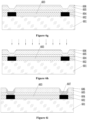
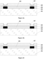
- Figure 6 shows schematic structural diagrams in a processing flow of a method for manufacturing a thin film bulk acoustic resonator according to an embodiment of the present disclosure. As shown in Figure 6 , the method includes processes as follows.
- a silicon layer 602 is grown on a substrate 601.
- the substrate 601 may be made of Si, SiC, sapphire, spinel, or the like.
- the silicon layer is grown through physical vapor deposition (PVD) and has a thickness ranging from 1.5 ⁇ m to 3 ⁇ m.
- PVD physical vapor deposition
- a required pattern of the cavity of the resonator is formed on the silicon layer 602 through photolithography, as shown in Figure 6b .
- a sacrificial layer 603 is grown in the cavity and then subject to chemical-mechanical polishing, as shown in Figure 6c .
- the sacrificial layer may be made of phosphosilicate glass (PSG, p-doped SiO 2 ).
- a bottom electrode 604 is provided on the silicon layer 602 and the sacrificial layer 603, and the bottom electrode 604 may be made of molybdenum.
- a piezoelectric layer 605 is provided on a basis of the bottom electrode 604, and the piezoelectric layer 605 is made of aluminum nitride. Specific structures refer to Figures 6d and 6e .
- a hard mask 606 is deposited on a surface of the piezoelectric layer 605 through chemical vapor deposition (CVD).
- the hard mask 606 is an inorganic thin film made of, for example, TiN, SiN, SiO 2 , or the like.
- An opening is formed in the hard mask through photolithography and etching.
- a shape of the hard mask is same as that of the top electrode which is subsequently formed, and a region blocked by the hard mask is an effective region of the resonator.
- a photoresist may be developed to form a pattern of the opening directly (that is, the hard mask is replaced with the photoresist), which can also achieve the technical effect of embodiments of the present disclosure.
- Ion implantation is performed on a region of the piezoelectric layer 605 exposed from the hard mask 606.
- Implanted atoms may be Ni, Fe, Cr, Mn, Co, V, Y, Si, or the like.
- the piezoelectric layer 605 is annealed after the ion implantation, and the annealing temperature should be higher than the Curie point of the material of the piezoelectric layer 605 after the ion implantation. Thereby, the ion-implanted region of the piezoelectric layer 605 forms a depolarized portion 607.
- a type and/or concentration of the implanted ions may be controlled in the ion implantation, such that the material of the piezoelectric layer after the ion implantation has a Curie point lower than the highest temperature occurring in processes which are for manufacturing the resonator and subsequent to the ion implantation.
- the piezoelectric layer 605 is subject to the ion implantation and then selective depolarization, in order to eliminate piezoelectricity of the piezoelectric layer 605.
- a Curie point for the piezoelectric layer 605 made of aluminum nitride is 673.15K (400°C), which is studied as a critical point.
- the Curie point of the piezoelectric layer 605 is lower than 673.15K and temperatures in multiple processes subsequent to the ion implantation exceed 673.15K, the temperatures are higher than the Curie point of the piezoelectric layer 605, which leads to violent movement and thus irregular arrangement of molecules and atoms within the film of the piezoelectric layer 605.
- these processes having higher temperatures can eliminate the piezoelectricity of the piezoelectric layer 605.
- the piezoelectric layer 605 is further annealed as an additional process after the ion implantation, and a temperature of the annealing should be higher than the Curie point of the piezoelectric layer 605.
- a preferable temperature of the annealing may be 10°C to 20°C higher than the Curie point of the piezoelectric layer 605, and such temperature is maintained for about 0.5h.
- the piezoelectric layer 605 may be doped with chromium.
- the Curie point of the piezoelectric layer 605 is slightly higher than 350K in a case that a concentration of chromium ranges from 1% to 3%, and is slightly higher than 400K in a case that the concentration of chromium is 15%. In such cases, the Curie point is lower than the foregoing critical point (673.15K), and therefore the annealing is not required.
- the Curie point is slightly higher than 900K. In such case, the Curie point is higher than the critical point, and hence it is necessary to anneal under a temperature higher than 900K, in order to eliminate the piezoelectricity of the depolarized portion 607.
- the piezoelectric layer 605 may be doped with vanadium. In a case that a concentration of vanadium is 1.58%, the piezoelectric layer 605 may have a Curie point of 300K, which is close to room temperature. In such case, the piezoelectricity of the depolarized portion 607 can be eliminated in subsequent processes without annealing.
- the hard mask 606 is removed by using hydrofluoric acid solution. Regardless of a contour of a region having implanted ions, such region does not extend out of a region defined by the cavity. That is, a vertical projection of the region having implanted ions may partially overlap with the boundary of the cavity. Alternatively, the vertical projection may extend slightly into the cavity.
- the region having implanted ions is limited in a horizontal direction as follows.
- the region may be the whole region outside the cavity or the cavities (as shown in Figure 6j ) or only a part of the region outside the cavity or the cavities (as shown in Figure 6k ).
- the region having implanted ions is limited in a vertical direction as follows.
- the region may penetrate the piezoelectric layer (as shown in Figure 6j ) or be partially implemented (as shown in Figure 61 ).
- a range along the horizontal direction may be tuned by adjusting a contour of the pattern for the opening in the hard mask 606, and a range along the vertical direction may be tuned by adjusting a parameter of the ion implantation.
- a larger region having implanted ions can improve device performances more greatly while increasing a cost. Therefore, an appropriate region for ion implantation may be determined based on a balance between a requirement on the cost and a requirement on device performances.
- the ion implantation may be performed on the whole non-resonating region to eliminate the piezoelectricity of the piezoelectric layer 605.
- the piezoelectricity of the piezoelectric layer 605 is only retained within the resonating region to achieve functions of the device. Thereby, maximum isolation and a minimum parasitic effect are realized.
- all regions are doped except a part of the piezoelectric layer 605 corresponding to the top electrode 608.
- the doped region is determined to achieve a depolarized portion, which is capable of suppressing parasitic oscillation on requirement, at a minimum cost.
- the doped region in the piezoelectric layer 605 may be arbitrarily configured with respect to its position among the resonators, its area, its depth, and its position outside the resonators.
- a top electrode 608 is provided on a surface of the piezoelectric layer 605, and the top electrode 608 is made of molybdenum.
- the sacrificial layer 603 is removed by using a hydrofluoric acid etchant to obtain a cavity 609. Thereby, a process of manufacturing the thin film bulk acoustic resonator is completed.
- the piezoelectric layer to be depolarized is exposed through depositing the hard mask 606, and selective depolarization can be adopted on the piezoelectric layer 605 through the ion implantation to eliminate the piezoelectricity of a part of the piezoelectric layer.
- the region for the ion implantation may be determined based on both the cost and device performances, and hence the process is applicable to various techniques for manufacturing thin film bulk acoustic resonators.
- the thin film bulk acoustic resonators manufactured through the method as shown in Figure 6a to Figure 6o utilizes depolarized piezoelectric layer at a specific area or a specific depth.
- the piezoelectric layer converts electrical energy into mechanical energy which is in a transverse-wave vibration mode and a longitudinal-wave vibration mode.
- the depolarized region can restrain the energy in the resonating region above the cavity of the resonator from dissipating via transverse waves. Hence, an intensity of mechanical vibration in the resonating region is ensured, and the Q factor of the resonator is improved.
- the piezoelectric layer in a specific region is depolarized and therefore has no piezoelectricity, which can suppress parasitic oscillation, restrain energy from dissipating via transverse waves. Hence, the Q factor and the device performances are improved.
- the manufacturing is simple, has a low cost, and is applicable to large-scale industrial production.
Landscapes
- Physics & Mathematics (AREA)
- Acoustics & Sound (AREA)
- Engineering & Computer Science (AREA)
- Manufacturing & Machinery (AREA)
- Piezo-Electric Or Mechanical Vibrators, Or Delay Or Filter Circuits (AREA)
Applications Claiming Priority (2)
| Application Number | Priority Date | Filing Date | Title |
|---|---|---|---|
| CN202010526851.5A CN111817679B (zh) | 2020-06-09 | 2020-06-09 | 一种薄膜体声波谐振器及其制作工艺 |
| PCT/CN2020/098557 WO2021248572A1 (fr) | 2020-06-09 | 2020-06-28 | Résonateur acoustique de volume à film mince et son procédé de fabrication |
Publications (2)
| Publication Number | Publication Date |
|---|---|
| EP4164126A1 true EP4164126A1 (fr) | 2023-04-12 |
| EP4164126A4 EP4164126A4 (fr) | 2023-11-22 |
Family
ID=72845796
Family Applications (1)
| Application Number | Title | Priority Date | Filing Date |
|---|---|---|---|
| EP20939534.2A Withdrawn EP4164126A4 (fr) | 2020-06-09 | 2020-06-28 | Résonateur acoustique de volume à film mince et son procédé de fabrication |
Country Status (6)
| Country | Link |
|---|---|
| US (1) | US11901872B2 (fr) |
| EP (1) | EP4164126A4 (fr) |
| JP (1) | JP2023522485A (fr) |
| KR (1) | KR20230007552A (fr) |
| CN (1) | CN111817679B (fr) |
| WO (1) | WO2021248572A1 (fr) |
Families Citing this family (11)
| Publication number | Priority date | Publication date | Assignee | Title |
|---|---|---|---|---|
| CN112260659B (zh) * | 2020-10-26 | 2022-02-01 | 武汉大学 | 一种高q值薄膜体声波谐振器及其制备方法 |
| CN113965182B (zh) * | 2021-12-23 | 2022-04-01 | 深圳新声半导体有限公司 | 一种提高体声波滤波器制备良率的方法和结构 |
| CN114389565A (zh) * | 2021-12-24 | 2022-04-22 | 杭州星阖科技有限公司 | 一种体声波谐振器及其制造方法 |
| US20230275553A1 (en) * | 2022-02-28 | 2023-08-31 | Texas Instruments Incorporated | Recessed frames in thickness mode piezoelectric resonators |
| CN117013982B (zh) * | 2022-04-29 | 2024-08-27 | 锐石创芯(重庆)科技有限公司 | 体声波谐振器、滤波器、多工器及其制作方法 |
| CN114826191B (zh) * | 2022-05-23 | 2023-11-07 | 武汉敏声新技术有限公司 | 一种薄膜体声波谐振器 |
| CN115242211A (zh) * | 2022-08-01 | 2022-10-25 | 上海芯波电子科技有限公司 | 一种机械波谐振器的性能提升方法 |
| CN115701269A (zh) * | 2022-11-01 | 2023-02-07 | 国网智能电网研究院有限公司 | 一种柔性压电能量收集器及其制备方法 |
| CN116032236B (zh) * | 2023-02-15 | 2023-06-06 | 成都频岢微电子有限公司 | 一种体声波耳形通道谐振器 |
| CN116582099A (zh) * | 2023-04-14 | 2023-08-11 | 见闻录(浙江)半导体有限公司 | 体声波谐振器及其组件和制作方法、电子设备、滤波器 |
| CN117375560B (zh) * | 2023-10-09 | 2024-07-16 | 武汉敏声新技术有限公司 | 一种体声波谐振器件及其制备方法 |
Family Cites Families (24)
| Publication number | Priority date | Publication date | Assignee | Title |
|---|---|---|---|---|
| DE69714909T2 (de) * | 1996-05-27 | 2003-04-30 | Ngk Insulators, Ltd. | Piezoelektrisches Element des Dünnschichttyps |
| JP4359915B2 (ja) * | 2003-08-21 | 2009-11-11 | 京セラ株式会社 | 圧電磁器振動体及び圧電共振装置 |
| JP4657660B2 (ja) * | 2003-09-12 | 2011-03-23 | パナソニック株式会社 | 薄膜バルク音響共振器、その製造方法、フィルタ、複合電子部品および通信機器 |
| US7230511B2 (en) * | 2003-09-12 | 2007-06-12 | Matsushita Electric Industrial Co., Ltd. | Thin film bulk acoustic resonator, method for producing the same, filter, composite electronic component device, and communication device |
| CN100488042C (zh) * | 2004-09-07 | 2009-05-13 | 株式会社村田制作所 | 制造压电谐振器的方法 |
| JP2007048816A (ja) * | 2005-08-08 | 2007-02-22 | Seiko Epson Corp | アクチュエータ装置の製造方法及びアクチュエータ装置並びに液体噴射ヘッド及び液体噴射装置 |
| CN102670259A (zh) * | 2006-11-03 | 2012-09-19 | 研究三角协会 | 使用挠曲模式压电换能器的增强的超声成像探头 |
| JP2008211396A (ja) * | 2007-02-23 | 2008-09-11 | Matsushita Electric Works Ltd | 圧電性薄膜の製造方法、共振装置およびそれを用いたuwb用フィルタ |
| JP5080858B2 (ja) | 2007-05-17 | 2012-11-21 | 太陽誘電株式会社 | 圧電薄膜共振器およびフィルタ |
| US8330325B1 (en) | 2011-06-16 | 2012-12-11 | Avago Technologies Wireless Ip (Singapore) Pte. Ltd. | Bulk acoustic resonator comprising non-piezoelectric layer |
| JP6414728B2 (ja) * | 2014-06-16 | 2018-10-31 | 株式会社リコー | 電気機械変換部材、液滴吐出ヘッド、画像形成装置、及び、電気機械変換素子の分極処理方法、及び、電気機械変換部材の製造方法 |
| US20160197593A1 (en) * | 2015-01-06 | 2016-07-07 | Zhuhai Advanced Chip Carriers & Electronic Substrate Solutions Technologies Co. Ltd. | Method for fabricating film bulk acoustic resonator filters |
| US10985732B2 (en) * | 2016-03-11 | 2021-04-20 | Akoustis, Inc. | 5.6 GHz Wi-Fi acoustic wave resonator RF filter circuit |
| US10720900B2 (en) * | 2016-07-07 | 2020-07-21 | Samsung Electro-Mechanics Co., Ltd. | Acoustic resonator and method |
| US10110188B2 (en) * | 2016-11-02 | 2018-10-23 | Akoustis, Inc. | Structure and method of manufacture for acoustic resonator or filter devices using improved fabrication conditions and perimeter structure modifications |
| US20180183405A1 (en) * | 2016-12-23 | 2018-06-28 | Avago Technologies General Ip (Singapore) Pte. Ltd | Bulk baw resonator having electrically insulating substrate |
| DE102017105432B3 (de) | 2017-03-14 | 2018-08-23 | Friedrich-Alexander-Universtität Erlangen-Nürnberg | Resonator und Verfahren zum Bereitstellen eines Resonators |
| CN107800396A (zh) * | 2017-11-27 | 2018-03-13 | 中电科技德清华莹电子有限公司 | 一种采用压电单晶箔的固贴型薄膜体声波谐振器及制备方法 |
| FR3076126A1 (fr) | 2017-12-26 | 2019-06-28 | Commissariat A L'energie Atomique Et Aux Energies Alternatives | Procede de realisation d'un resonateur acoustique a ondes de volume a capacite parasite reduite |
| CN108173531B (zh) * | 2018-02-08 | 2024-11-12 | 武汉衍熙微器件有限公司 | 一种体声波谐振器与表面声波谐振器的混合式声波谐振器 |
| CN113519119B (zh) * | 2018-08-20 | 2025-02-14 | D·伍尔西 | 声谐振器 |
| KR20200030478A (ko) | 2018-09-12 | 2020-03-20 | 스카이워크스 글로벌 피티이. 엘티디. | 벌크 음향파 공진기를 위한 리세스 프레임 구조체 |
| CN109546985A (zh) * | 2018-11-02 | 2019-03-29 | 天津大学 | 体声波谐振器及其制造方法 |
| CN110767606B (zh) * | 2019-12-24 | 2020-04-17 | 杭州见闻录科技有限公司 | 一种具有复合功能的电子元器件及其制造方法 |
-
2020
- 2020-06-09 CN CN202010526851.5A patent/CN111817679B/zh active Active
- 2020-06-28 JP JP2022574755A patent/JP2023522485A/ja active Pending
- 2020-06-28 US US18/007,994 patent/US11901872B2/en active Active
- 2020-06-28 KR KR1020227045935A patent/KR20230007552A/ko not_active Ceased
- 2020-06-28 EP EP20939534.2A patent/EP4164126A4/fr not_active Withdrawn
- 2020-06-28 WO PCT/CN2020/098557 patent/WO2021248572A1/fr not_active Ceased
Also Published As
| Publication number | Publication date |
|---|---|
| WO2021248572A1 (fr) | 2021-12-16 |
| CN111817679B (zh) | 2021-10-15 |
| US11901872B2 (en) | 2024-02-13 |
| KR20230007552A (ko) | 2023-01-12 |
| CN111817679A (zh) | 2020-10-23 |
| US20230208383A1 (en) | 2023-06-29 |
| JP2023522485A (ja) | 2023-05-30 |
| EP4164126A4 (fr) | 2023-11-22 |
Similar Documents
| Publication | Publication Date | Title |
|---|---|---|
| US11901872B2 (en) | Thin film bulk acoustic resonator and manufacturing process therefor | |
| US20210013859A1 (en) | Transversely-excited film bulk acoustic resonator with etched conductor patterns | |
| US11811391B2 (en) | Transversely-excited film bulk acoustic resonator with etched conductor patterns | |
| US9197185B2 (en) | Resonator device including electrodes with buried temperature compensating layers | |
| US9479139B2 (en) | Resonator device including electrode with buried temperature compensating layer | |
| WO2021258405A1 (fr) | Résonateur acoustique de volume à film mince et son procédé de fabrication | |
| Rassay et al. | Intrinsically switchable ferroelectric scandium aluminum nitride lamb-mode resonators | |
| JP6371518B2 (ja) | 圧電薄膜共振器およびその製造方法、フィルタ並びにデュプレクサ | |
| US20140292149A1 (en) | Temperature compensated acoustic resonator device | |
| JP2008072691A (ja) | 共振器、それを備えた装置、および共振器の製造方法 | |
| JPWO2007119643A1 (ja) | 圧電薄膜共振子、圧電薄膜デバイスおよびその製造方法 | |
| WO2022017486A1 (fr) | Résonateur réglable et son procédé de fabrication | |
| JP2009290371A (ja) | Baw共振装置 | |
| US12323130B2 (en) | Transversely-excited film bulk acoustic resonator with controlled conductor sidewall angles | |
| CN116073785A (zh) | 用于耦合优化的介电涂覆的横向激发薄膜体声学谐振器(xbar) | |
| JP4373936B2 (ja) | 薄膜圧電共振器及びその製造方法 | |
| CN113630099A (zh) | 体声波谐振器及制造方法、体声波谐振器组件、滤波器及电子设备 | |
| JP2008211392A (ja) | 共振器及びその製造方法 | |
| CN117856757A (zh) | 体声波谐振器的制作方法 | |
| JP2019016827A (ja) | 圧電薄膜共振器およびその製造方法、フィルタ並びにマルチプレクサ | |
| JP2008211396A (ja) | 圧電性薄膜の製造方法、共振装置およびそれを用いたuwb用フィルタ | |
| KR20170096717A (ko) | 음향 공진기 | |
| JP2009124696A (ja) | 共振装置 | |
| JP4797772B2 (ja) | Baw共振器 | |
| JP2009290367A (ja) | Baw共振装置およびその製造方法 |
Legal Events
| Date | Code | Title | Description |
|---|---|---|---|
| STAA | Information on the status of an ep patent application or granted ep patent |
Free format text: STATUS: THE INTERNATIONAL PUBLICATION HAS BEEN MADE |
|
| PUAI | Public reference made under article 153(3) epc to a published international application that has entered the european phase |
Free format text: ORIGINAL CODE: 0009012 |
|
| STAA | Information on the status of an ep patent application or granted ep patent |
Free format text: STATUS: REQUEST FOR EXAMINATION WAS MADE |
|
| 17P | Request for examination filed |
Effective date: 20221201 |
|
| AK | Designated contracting states |
Kind code of ref document: A1 Designated state(s): AL AT BE BG CH CY CZ DE DK EE ES FI FR GB GR HR HU IE IS IT LI LT LU LV MC MK MT NL NO PL PT RO RS SE SI SK SM TR |
|
| DAV | Request for validation of the european patent (deleted) | ||
| DAX | Request for extension of the european patent (deleted) | ||
| A4 | Supplementary search report drawn up and despatched |
Effective date: 20231025 |
|
| RIC1 | Information provided on ipc code assigned before grant |
Ipc: H03H 9/60 20060101ALN20231019BHEP Ipc: H03H 9/58 20060101ALN20231019BHEP Ipc: H03H 9/17 20060101ALN20231019BHEP Ipc: H03H 9/05 20060101ALN20231019BHEP Ipc: H03H 9/02 20060101ALI20231019BHEP Ipc: H03H 3/02 20060101AFI20231019BHEP |
|
| STAA | Information on the status of an ep patent application or granted ep patent |
Free format text: STATUS: EXAMINATION IS IN PROGRESS |
|
| 17Q | First examination report despatched |
Effective date: 20240415 |
|
| STAA | Information on the status of an ep patent application or granted ep patent |
Free format text: STATUS: THE APPLICATION IS DEEMED TO BE WITHDRAWN |
|
| 18D | Application deemed to be withdrawn |
Effective date: 20250318 |