EP4167050B1 - Appareil électronique comprenant un écran souple - Google Patents
Appareil électronique comprenant un écran souple Download PDFInfo
- Publication number
- EP4167050B1 EP4167050B1 EP21842226.9A EP21842226A EP4167050B1 EP 4167050 B1 EP4167050 B1 EP 4167050B1 EP 21842226 A EP21842226 A EP 21842226A EP 4167050 B1 EP4167050 B1 EP 4167050B1
- Authority
- EP
- European Patent Office
- Prior art keywords
- circuit board
- electronic device
- module
- disposed
- display
- Prior art date
- Legal status (The legal status is an assumption and is not a legal conclusion. Google has not performed a legal analysis and makes no representation as to the accuracy of the status listed.)
- Active
Links
Images










Classifications
-
- G—PHYSICS
- G06—COMPUTING OR CALCULATING; COUNTING
- G06F—ELECTRIC DIGITAL DATA PROCESSING
- G06F1/00—Details not covered by groups G06F3/00 - G06F13/00 and G06F21/00
- G06F1/16—Constructional details or arrangements
- G06F1/1613—Constructional details or arrangements for portable computers
- G06F1/1633—Constructional details or arrangements of portable computers not specific to the type of enclosures covered by groups G06F1/1615 - G06F1/1626
- G06F1/1675—Miscellaneous details related to the relative movement between the different enclosures or enclosure parts
- G06F1/1681—Details related solely to hinges
-
- H—ELECTRICITY
- H04—ELECTRIC COMMUNICATION TECHNIQUE
- H04M—TELEPHONIC COMMUNICATION
- H04M1/00—Substation equipment, e.g. for use by subscribers
- H04M1/02—Constructional features of telephone sets
- H04M1/0202—Portable telephone sets, e.g. cordless phones, mobile phones or bar type handsets
- H04M1/0206—Portable telephones comprising a plurality of mechanically joined movable body parts, e.g. hinged housings
- H04M1/0208—Portable telephones comprising a plurality of mechanically joined movable body parts, e.g. hinged housings characterized by the relative motions of the body parts
- H04M1/0235—Slidable or telescopic telephones, i.e. with a relative translation movement of the body parts; Telephones using a combination of translation and other relative motions of the body parts
- H04M1/0237—Sliding mechanism with one degree of freedom
-
- H—ELECTRICITY
- H04—ELECTRIC COMMUNICATION TECHNIQUE
- H04M—TELEPHONIC COMMUNICATION
- H04M1/00—Substation equipment, e.g. for use by subscribers
- H04M1/02—Constructional features of telephone sets
- H04M1/0202—Portable telephone sets, e.g. cordless phones, mobile phones or bar type handsets
- H04M1/026—Details of the structure or mounting of specific components
-
- H—ELECTRICITY
- H04—ELECTRIC COMMUNICATION TECHNIQUE
- H04M—TELEPHONIC COMMUNICATION
- H04M1/00—Substation equipment, e.g. for use by subscribers
- H04M1/02—Constructional features of telephone sets
- H04M1/0202—Portable telephone sets, e.g. cordless phones, mobile phones or bar type handsets
- H04M1/026—Details of the structure or mounting of specific components
- H04M1/0262—Details of the structure or mounting of specific components for a battery compartment
-
- H—ELECTRICITY
- H04—ELECTRIC COMMUNICATION TECHNIQUE
- H04M—TELEPHONIC COMMUNICATION
- H04M1/00—Substation equipment, e.g. for use by subscribers
- H04M1/02—Constructional features of telephone sets
- H04M1/0202—Portable telephone sets, e.g. cordless phones, mobile phones or bar type handsets
- H04M1/026—Details of the structure or mounting of specific components
- H04M1/0266—Details of the structure or mounting of specific components for a display module assembly
- H04M1/0268—Details of the structure or mounting of specific components for a display module assembly including a flexible display panel
-
- H—ELECTRICITY
- H04—ELECTRIC COMMUNICATION TECHNIQUE
- H04M—TELEPHONIC COMMUNICATION
- H04M1/00—Substation equipment, e.g. for use by subscribers
- H04M1/02—Constructional features of telephone sets
- H04M1/0202—Portable telephone sets, e.g. cordless phones, mobile phones or bar type handsets
- H04M1/026—Details of the structure or mounting of specific components
- H04M1/0277—Details of the structure or mounting of specific components for a printed circuit board assembly
-
- G—PHYSICS
- G06—COMPUTING OR CALCULATING; COUNTING
- G06F—ELECTRIC DIGITAL DATA PROCESSING
- G06F1/00—Details not covered by groups G06F3/00 - G06F13/00 and G06F21/00
- G06F1/16—Constructional details or arrangements
- G06F1/1613—Constructional details or arrangements for portable computers
- G06F1/1615—Constructional details or arrangements for portable computers with several enclosures having relative motions, each enclosure supporting at least one I/O or computing function
- G06F1/1624—Constructional details or arrangements for portable computers with several enclosures having relative motions, each enclosure supporting at least one I/O or computing function with sliding enclosures, e.g. sliding keyboard or display
-
- G—PHYSICS
- G06—COMPUTING OR CALCULATING; COUNTING
- G06F—ELECTRIC DIGITAL DATA PROCESSING
- G06F1/00—Details not covered by groups G06F3/00 - G06F13/00 and G06F21/00
- G06F1/16—Constructional details or arrangements
- G06F1/1613—Constructional details or arrangements for portable computers
- G06F1/1633—Constructional details or arrangements of portable computers not specific to the type of enclosures covered by groups G06F1/1615 - G06F1/1626
- G06F1/1635—Details related to the integration of battery packs and other power supplies such as fuel cells or integrated AC adapter
-
- G—PHYSICS
- G06—COMPUTING OR CALCULATING; COUNTING
- G06F—ELECTRIC DIGITAL DATA PROCESSING
- G06F1/00—Details not covered by groups G06F3/00 - G06F13/00 and G06F21/00
- G06F1/16—Constructional details or arrangements
- G06F1/1613—Constructional details or arrangements for portable computers
- G06F1/1633—Constructional details or arrangements of portable computers not specific to the type of enclosures covered by groups G06F1/1615 - G06F1/1626
- G06F1/1637—Details related to the display arrangement, including those related to the mounting of the display in the housing
- G06F1/1652—Details related to the display arrangement, including those related to the mounting of the display in the housing the display being flexible, e.g. mimicking a sheet of paper, or rollable
-
- G—PHYSICS
- G06—COMPUTING OR CALCULATING; COUNTING
- G06F—ELECTRIC DIGITAL DATA PROCESSING
- G06F1/00—Details not covered by groups G06F3/00 - G06F13/00 and G06F21/00
- G06F1/16—Constructional details or arrangements
- G06F1/1613—Constructional details or arrangements for portable computers
- G06F1/1633—Constructional details or arrangements of portable computers not specific to the type of enclosures covered by groups G06F1/1615 - G06F1/1626
- G06F1/1684—Constructional details or arrangements related to integrated I/O peripherals not covered by groups G06F1/1635 - G06F1/1675
- G06F1/1686—Constructional details or arrangements related to integrated I/O peripherals not covered by groups G06F1/1635 - G06F1/1675 the I/O peripheral being an integrated camera
-
- G—PHYSICS
- G06—COMPUTING OR CALCULATING; COUNTING
- G06F—ELECTRIC DIGITAL DATA PROCESSING
- G06F1/00—Details not covered by groups G06F3/00 - G06F13/00 and G06F21/00
- G06F1/16—Constructional details or arrangements
- G06F1/1613—Constructional details or arrangements for portable computers
- G06F1/1633—Constructional details or arrangements of portable computers not specific to the type of enclosures covered by groups G06F1/1615 - G06F1/1626
- G06F1/1684—Constructional details or arrangements related to integrated I/O peripherals not covered by groups G06F1/1635 - G06F1/1675
- G06F1/1698—Constructional details or arrangements related to integrated I/O peripherals not covered by groups G06F1/1635 - G06F1/1675 the I/O peripheral being a sending/receiving arrangement to establish a cordless communication link, e.g. radio or infrared link, integrated cellular phone
-
- G—PHYSICS
- G09—EDUCATION; CRYPTOGRAPHY; DISPLAY; ADVERTISING; SEALS
- G09F—DISPLAYING; ADVERTISING; SIGNS; LABELS OR NAME-PLATES; SEALS
- G09F9/00—Indicating arrangements for variable information in which the information is built-up on a support by selection or combination of individual elements
- G09F9/30—Indicating arrangements for variable information in which the information is built-up on a support by selection or combination of individual elements in which the desired character or characters are formed by combining individual elements
- G09F9/301—Indicating arrangements for variable information in which the information is built-up on a support by selection or combination of individual elements in which the desired character or characters are formed by combining individual elements flexible foldable or roll-able electronic displays, e.g. thin LCD, OLED
-
- H—ELECTRICITY
- H04—ELECTRIC COMMUNICATION TECHNIQUE
- H04M—TELEPHONIC COMMUNICATION
- H04M1/00—Substation equipment, e.g. for use by subscribers
- H04M1/02—Constructional features of telephone sets
- H04M1/0202—Portable telephone sets, e.g. cordless phones, mobile phones or bar type handsets
- H04M1/026—Details of the structure or mounting of specific components
- H04M1/0264—Details of the structure or mounting of specific components for a camera module assembly
Definitions
- Various embodiments of the invention described herein relate to an electronic device including a flexible display.
- An electronic device may include a flexible display.
- the electronic device may expand a display area visually exposed on the exterior of the electronic device.
- the flexible display may be disposed in a curved, foldable, or rollable form in the electronic device.
- US2019268455A1 relates to an electronic device which includes an assembly that enables varying a visible portion of a display by extending and retracting a bendable portion of the display.
- the extending and retracting of the bendable display is facilitated by a first assembly on which a substantially planar visible portion of the display is disposed and a second assembly slidably attached to the first assembly.
- the electronic devices may include an electronic device of a slidable type in which a fixed structure and a sliding structure are developed relative to each other in a sliding manner or an electronic device of a foldable type in which a first housing and a second housing are disposed to be folded or unfolded.
- the sliding structure may move relative to the fixed structure, and accordingly an area of a flexible display exposed on a front side of the electronic device may be expanded or reduced.
- the electronic device of the slidable type may include a multi-bar that supports the display and a guide rail that guides a movement of the multi-bar.
- the guide rail may be located in a lateral direction of the electronic device.
- the guide rail may be disposed to face a side cover that operates as an antenna radiator of the electronic device.
- Various embodiments of the disclosure provide an electronic device in which to use a side cover as an antenna radiator of the electronic device, at least part of the side cover passes through a guide rail to implement an antenna contact structure.
- An electronic device according to claim 1 is provided by the invention.
- the electronic device may use the side cover as an antenna radiator by providing an antenna contact through the flange (e.g., the protruding portion) of the side cover that passes through at least part of the guide rail.
- the flange e.g., the protruding portion
- the first structure 110 may form at least part of the exterior (or, the outer surface) of the electronic device 100.
- the first structure 110 may form the rear side and a part of lateral sides of the electronic device 100.
- the first structure 110 may provide a space in which other components of the electronic device 100 are supported and/or disposed.
- the battery 192 may be, and the plurality of circuit boards 210 are, disposed inside the first structure 110.
- the second structure 160 may be slidably supported on part (e.g., a bracket 140) of the first structure 110.
- the first structure 110 may include a rear member 120, a side member 130, the bracket 140, and a guide member 150.
- the rear member 120, the side member 130, the bracket 140, and the guide member 150 may be fixed structures that are the basis of a relative movement of the second structure 160.
- the second structure 160 may slide in the opposite directions relative to the rear member 120, the side member 130, the bracket 140, and the guide member 150.
- the first structure 110 may be formed through a coupling structure of the rear member 120, the side member 130, the bracket 140, and the guide member 150.
- the rear member 120 and the side member 130 may form the rear side and a part of the lateral sides of the electronic device 100 and may form a predetermined space in which other components of the electronic device 100 are disposed.
- the first structure 110 may be configured such that the rear member 120, the side member 130, the bracket 140, and the guide member 150 are assembled together.
- at least some of the rear member 120, the side member 130, the bracket 140, and the guide member 150 may be integrally formed.
- the rear member 120 may include a back cover 121 forming the rear side of the electronic device 100 and a rear case 122 disposed on one surface of the back cover 121.
- the rear case 122 may be disposed on an upper surface (e.g., a surface facing the +Z-axis direction) of the back cover 121 to support the plurality of circuit boards 210 and/or the battery 192 disposed inside the first structure 110.
- the rear case 122 may be located to face the bracket 140 with the plurality of circuit boards 210 and the battery 192 therebetween.
- the camera decoration member 124 may be disposed on the back cover 121.
- the back cover 121 may have, in a partial area thereof, an opening area 123 into which part of the camera decoration member 124 is inserted.
- the camera decoration member 124 may be exposed on the rear side of the electronic device 100 through the opening area 123.
- the plurality of rear cameras 320 disposed inside the electronic device 100 may be configured to receive light from outside the electronic device 100 through a transparent and/or translucent area of the camera decoration member 124.
- the side member 130 may be located on opposite longitudinal end portions of the rear member 120 to form a part of the lateral sides of the electronic device 100.
- the side member 130 may form a lateral side facing the Y-axis direction among the lateral sides of the electronic device 100.
- the side member 130 may include a first side member 131 located on an end portion of the rear member 120 that faces the + Y-axis direction and a second side member 132 located on an end portion of the rear member 120 that faces the -Y-axis direction.
- the side member 130 may be coupled to the bracket 140.
- the side member 130 may be fixed to the bracket 140 through screw coupling.
- the first side member 131 may include the first side cover 133 coupled to a first edge portion 143 (e.g., an edge portion facing the +Y-axis direction) of the bracket 140 that is parallel to the sliding directions D1 and D2 and a first decoration member 134 coupled to the first side cover 133 to form an outer surface of the electronic device 100.
- the second side member 132 may include the second side cover 135 coupled to a second edge portion 144 (e.g., an edge portion facing the -Y-axis direction) that faces away from the first edge portion 143 and a second decoration member 136 coupled to the second side cover 135 to form an outer surface of the electronic device 100.
- the first decoration member 134 and the second decoration member 136 may improve the completeness and aesthetics of the electronic device 100 in appearance.
- the side decoration members 134 and 136 may hide screws and coupling holes when the side covers 133 and 135 are screw-coupled to the bracket 140.
- the side decoration members 134 and 136 may be integrally formed with the side covers 133 and 135.
- the bracket 140 may support other components included in the electronic device 100.
- the bracket 40 may be configured to support the display support member 193, the roller 191, the plurality of circuit boards 210, the battery 192, a front camera module 310, and the rear camera modules (not illustrated) (e.g., the plurality of rear cameras 320 of FIGS. 8A and 8B ).
- the bracket 140 may have a substantially plate shape and may be formed of a material having a specified stiffness.
- the bracket 140 may include a first surface 141 (e.g., a surface facing the +Z-axis direction) that faces toward the display support member 193 and a second surface (not illustrated) (e.g., a surface facing the -Z-axis direction) that faces away from the first surface 141.
- the second surface e.g., a second surface 142 of FIG. 4
- the battery 192 and the plurality of circuit boards 210 may face toward the battery 192 and the plurality of circuit boards 210.
- the bracket 140 may include the edge portions 143 and 144 to which the guide member 150 and the side member 130 are coupled.
- the edge portions 143 and 144 may extend parallel to the sliding directions D1 and D2 of the second structure 160.
- the edge portions 143 and 144 may include the first edge portion 143 to which a first guide member 151 and the first side member 131 are coupled and the second edge portion 144 to which a second guide member 152 and the second side member 132 are coupled.
- the side member 130 and the guide member 150 may be coupled to the edge portions 143 and 144 and may be fixedly disposed on the bracket 140 accordingly.
- the second structure 160 may be disposed on the first surface 141 of the bracket 140 so as to be movable in the sliding directions D1 and D2.
- the bracket 140 and the second structure 160 may be connected through the driving unit 180 disposed between the first surface 141 of the bracket 140 and the second structure 160.
- the second structure 160 may be configured to move in the sliding directions D1 and D2 over the first surface 141 of the bracket 140 by using an elastic force provided by the driving unit 180.
- the bracket 140 may support the plurality of circuit boards 210 and the battery 192.
- the bracket 140 may be disposed such that the second surface 142 faces the rear case 122 with the plurality of circuit boards 210 and the battery 192 therebetween.
- the plurality of circuit boards 210 and the battery 192 may be fixedly disposed between the second surface 142 of the bracket 140 and the rear case 122.
- the roller 191 may be rotatably coupled to one side of the bracket 140.
- the roller 191 may be disposed between the first edge portion 143 and the second edge portion 144 of the bracket 140 and may extend in a direction perpendicular to the sliding directions D1 and D2.
- roller coupling portions (not illustrated) to which the roller 191 is rotatably coupled may be formed on end portions of the first edge portion 143 and the second edge portion 144 that face the second direction D2.
- the guide member 150 guides movements of the display 170 and the display support member 193.
- the guide member 150 may be coupled to the edge portions 143 and 144 of the bracket 140.
- the guide member 150 may guide movements of the display 170 and the display support member 193 when the second structure 160 moves in a state of being fixed to the bracket 140.
- the guide member 150 includes guide grooves (not illustrated) (e.g., guide grooves 1521 of FIG. 21 ) into which opposite end portions of the display support member 193 in the lengthwise direction (e.g., the Y-axis direction) are slidably inserted.
- the guide member 150 may guide a movement of the display support member 193 along a predetermined path (or, track) corresponding to the guide grooves and may support the display support member 193 such that the display support member 193 remains flat.
- the display support member 193 may move along the guide grooves in the state in which the opposite longitudinal end portions of the display support member 193 are inserted into the guide grooves.
- the guide member 150 may include the first guide member 151 coupled to the first edge portion 143 of the bracket 140 and the second guide member 152 coupled to the second edge portion 144 of the bracket 140.
- the first guide member 151 may be located between the first edge portion 143 and the first side member 131.
- the second guide member 152 may be located between the second edge portion 144 and the second side member 132.
- the side member 130 and the guide member 150 may be assembled as separate components. However, this is illustrative, and according to various embodiments, the guide member 150 may be integrally formed with the side member 130.
- the driving unit 180 may provide a driving force to change the electronic device 100 to the first state 101 or the second state 102.
- the driving unit 180 may be disposed between the second structure 160 and the bracket 140.
- One end portion of the driving unit 180 may be coupled to the first surface 141 of the bracket 140, and an opposite end portion of the driving unit 180 may be coupled to the fourth surface 164b of the second structure 160.
- the driving unit 180 may connect the bracket 140 and the second structure 160.
- the driving unit 180 may be configured to provide a predetermined elastic force in a moving direction of the second structure 160 when the second structure 160 is moved by a specified distance or more in the sliding directions D1 and D2 by an external force of a user.
- the electronic device 100 may further include the front camera module 310 exposed on the front side (e.g., the side facing the +Z-axis direction) of the electronic device 100 and the rear camera modules (not illustrated) (e.g., the plurality of rear cameras 320 of FIGS. 8A and 8B ) exposed on the rear side (e.g., the side facing the -Z-axis direction) of the electronic device 100.
- the front camera module 310 exposed on the front side (e.g., the side facing the +Z-axis direction) of the electronic device 100 and the rear camera modules (not illustrated) (e.g., the plurality of rear cameras 320 of FIGS. 8A and 8B ) exposed on the rear side (e.g., the side facing the -Z-axis direction) of the electronic device 100.
- the front camera module 310 may be fixedly disposed on the second structure 160 to move together with the second structure 160.
- the front camera module 310 e.g., a punch hole camera
- the front camera module may be exposed on the front side of the electronic device 100 through the camera hole (not illustrated) of the second structure 160 and a partial area of the display 170.
- the front camera module e.g., an under display camera (UDC)
- UDC under display camera
- At least part of the front camera module 310 according to the other embodiment may be disposed under the display 170, and the front camera module 310 may be configured to take an image of a subject through part of an active area of the display 170.
- the front camera module 310 may not be visually exposed on an area of the display 170.
- the rear camera modules may be fixedly disposed in the first structure 110.
- the rear camera modules may be disposed on the bracket 140 and may be in a state of being fixed to the first structure 110, when the second structure 160 moves.
- the rear camera modules may be visually exposed on the rear side of the electronic device 100 through the camera decoration member 124 disposed on the rear member 120.
- the camera decoration member 124 may include a decorative structure 125 having a plurality of openings 1251 formed therein and a camera window 126 attached to the decorative structure 125.
- the rear camera modules may be disposed in the openings 1251 of the decorative structure 125.
- the camera window 126 may include a plurality of window areas 1261 corresponding to the openings 1251 of the decorative structure 125 such that the rear camera modules are capable of receiving light.
- the plurality of window areas 1261 may be disposed to overlap the plurality of openings 1251.
- the plurality of window areas 1261 may be formed to be transparent or translucent to allow light to transmit.
- the rear camera modules e.g., lenses
- the rear camera modules may be configured to receive light from the outside through the openings 1251 and the window areas 1261.
- the rear camera modules may include a plurality of camera modules (e.g., a dual camera or a triple camera).
- the rear camera modules are not necessarily limited to including the plurality of camera modules and may be implemented with one camera module according to an embodiment.
- the electronic device 100 illustrated in FIG. 3 may be an embodiment of a slidable (or, rollerable) electronic device, and structures of electronic devices 100 according to various embodiments of the disclosure are not limited to the illustrated embodiment.
- electronic devices 100 according to various embodiments of the disclosure may be implemented with various forms of slidable (or, rollable) electronic devices that include a fixed structure and a movable structure movable relative to the fixed structure and in which a display area is expanded or reduced as a flexible display moves together with the movable structure.
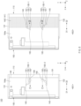
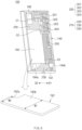
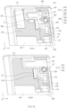
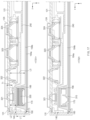
- FIG. 4 is a sectional view of the electronic device according to an embodiment.
- FIG. 4 is a sectional view illustrating the first state of the electronic device 100
- 402 of FIG. 4 is a sectional view illustrating the second state of the electronic device 100.
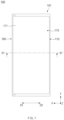
- 401 of FIG. 4 is a sectional view of the electronic device 100 taken along line S1-S1' in FIG. 1 .
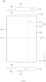
- 402 of FIG. 4 is a sectional view of the electronic device 100 taken along line S2-S2' in FIG. 2 .
- the electronic device 100 may include the first structure 110, the second structure 160, the display 170, the driving unit 180, the display support member 193, the roller 191 and the battery 192.
- the components of the electronic device 100 illustrated in FIG. 4 are identical or similar to some of the components of the electronic device 100 illustrated in FIGS. 1 to 3 , and repetitive descriptions will be omitted.
- the electronic device 100 may be changed to the first state (e.g., FIG. 1 or 401 of FIG. 4 ) and the second state (e.g., FIG. 2 or 402 of FIG. 4 ) by a sliding motion of the second structure 160 relative to the first structure 110.
- the first structure 110 may be a relatively fixed structure with respect to the sliding of the second structure 160.
- the first structure 110 may include the back cover 121, the rear case 122, and the bracket 140.
- the first structure 110 may further include a side member (e.g., the side member 130 of FIG. 3 ) and a guide member (e.g., the guide member 150 of FIG. 3 ).
- the second structure 160 may be disposed over the first surface 141 of the bracket 140 and may move in the first direction D1 or the second direction D2 relative to the back cover 121, the rear case 122, and the bracket 140.
- the bracket 140 may be disposed between the second structure 160 and the back cover 121.
- the bracket 140 may be disposed such that the first surface 141 faces toward the second structure 160 and the second surface 142 faces toward the back cover 121 or the rear case 122.
- the battery 192 may be disposed on the second surface 142 of the bracket 140.
- the battery 192 may be supported by the rear case 122 and the bracket 140.
- the roller 191 may be coupled to one side of the bracket 140 so as to be rotatable about an axis of rotation R.
- the second structure 160 may be configured to move in the first direction D1 or the second direction D2 relative to the bracket 140. For example, when the first area 171 of the display 170 is viewed from above, the second structure 160 may partially overlap the bracket 140. The size of the area by which the second structure 160 and the bracket 140 overlap each other may be changed in response to sliding of the second structure 160. For example, the area by which the second structure 160 and the bracket 140 overlap each other may be relatively smaller in the second state than in the first state.
- the fourth surface 164b of the second structure 160 may be exposed outside the electronic device 100 as the electronic device 100 is changed from the first state to the second state. For example, the fourth surface 164b of the second structure 160, together with the back cover 121, may form the rear side of the electronic device 100 in the second state or in the intermediate state between the first state and the second state.
- the display 170 may be disposed on the third surface 164a of the second structure 160.
- part of the first area 171 of the display 170 may be attached to the third surface 164a of the second structure 160, and thus the display 170 may move together when the second structure 160 moves.
- the second structure 160 may form substantially the same plane with part of the display support member 193.
- the second structure 160 may be connected with the bracket 140 through the driving unit 180.
- a second support portion 183 of the driving unit 180 may be coupled to the fourth surface 164b of the second structure 160, and a first support portion 181 of the driving unit 180 may be coupled to the first surface 141 of the bracket 140.
- the second structure 160 may be configured to move in the first direction D1 or the second direction D2 relative to the bracket 140 by using an elastic force provided by the driving unit 180.
- the display 170 may include the first area 171 exposed on the front side (e.g., the side facing the +Z-axis direction) of the electronic device 100 in the first state and the second area 173 extending from the first area 171.
- the second state at least part of the second area 173, together with the first area 171, may be exposed on the front side of the electronic device 100.
- the second area 173 in the first state, may be located inside the first structure 110, and in the second state, at least part of the second area 173 may move out of the first structure 110 and may be exposed on the front side of the electronic device 100.
- the first area 171 and the second area 173 of the display 170 may be distinguished from each other, depending on whether the first area 171 and the second area 173 are exposed on the front side of the electronic device 100 in the first state.
- the position of a dividing line between the first area 171 and the second area 173 is not limited to the specific position illustrated in FIG. 4 .
- the position of the dividing line between the first area 171 and the second area 173 may be changed accordingly.
- the first area 171 may include the rigid portion and part of the flexible portion, and the second area 173 may include the remaining part of the flexible portion.
- the entire display 170 may be formed of a flexible material.
- the display 170 may be formed such that rigid portions are located on opposite sides of a flexible portion.
- the driving unit 180 may be disposed between the second structure 160 and the bracket 140.
- the driving unit 180 may be disposed between the first surface 141 of the bracket 140 and the fourth surface 164b of the second structure 160.
- the driving unit 180 may be located to face the battery 192 with the bracket 140 therebetween.
- the driving unit 180 may generate elastic forces acting in directions parallel to the sliding directions D1 and D2 of the second structure 160.
- the driving unit 180 may include the first support portion 181, the second support portion 183, and an elastic portion 185.
- the elastic portion 185 may connect the first support portion 181 and the second support portion 183.
- the elastic portion 185 may be compressed or uncompressed depending on a relative movement of the first support portion 181 and the second support portion 183.
- the part of the display support member 193 may move into the space between the back cover 121 and the roller 191 (e.g., slide-in motion) as the roller 191 rotates in a second rotational direction (e.g., the clockwise direction) opposite to the first rotational direction.
- a second rotational direction e.g., the clockwise direction
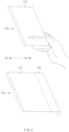
- FIG. 5 illustrates deformation of the electronic device according to an embodiment.
- FIG. 6 illustrates a motion of the driving unit of the electronic device according to an embodiment.
- FIG. 7 illustrates a motion of the driving unit of the electronic device according to an embodiment.
- the state of the electronic device 100 may be changed as an external force is applied to the display 170.
- the electronic device 100 may be configured (e.g., a semi-automatic open structure) such that when the electronic device 100 is changed to the first state or the second state, the second structure 160 is moved by an elastic force generated by the driving unit 180 even though the external force of the user is removed after the second structure 160 is moved by the external force F of the user by a specified distance or more.
- a semi-automatic open structure e.g., a semi-automatic open structure
- the electronic device 100 may include the first structure 110, the second structure 160, and the driving unit 180.
- the first structure 110 may include the first side member 131, the second side member 132, and the bracket 140.
- the bracket 140 and the second structure 160 may include the connecting shafts 145 and 165, respectively, to which the driving unit 180 is rotatably coupled.
- the bracket 140 may include the first connecting shaft 145 to which the first support portion 181 of the driving unit 180 is coupled.
- the second structure 160 may include the second connecting shaft 165 to which the second support portion 183 of the driving unit 180 is coupled.
- the first support portion 181 may be rotatably coupled to the first connecting shaft 145.
- the second support portion 183 may be rotatably connected to the second connecting shaft 165.
- first support portion 181 may be rotatably coupled to the first connecting shaft 145 of the bracket 140.
- the second support portion 183 may be rotatably coupled to the second connecting shaft 165 of the second structure 160.
- the first support portion 181 coupled to the first connecting shaft 145 may move together with the first connecting shaft 145, and the second support portion 183 coupled to the second connecting shaft 165 may move together with the second connecting shaft 165.
- the second support portion 183 may linearly move together with the second connecting shaft 165 in the sliding directions D1 and D2 when the second structure 160 moves relative to the bracket 140.
- the first support portion 181 may rotate about the first connecting shaft 145 when the second support portion 183 moves.
- the first support portion 181 may rotate about the first connecting shaft 145 in a predetermined range in a state in which a movement in the sliding directions D1 and D2 is limited.
- the second support portion 183 in the first state, may be located in the second direction D2 with respect to the first support portion 181. In the second state, the second support portion 183 may be located in the first direction D1 with respect to the first support portion 181.
- the shape of the driving unit 180 illustrated in 601 of FIG. 6 may be referred to as the shape of the driving unit 180 illustrated in 401 of FIG. 4
- the shape of the driving unit 180 illustrated in 602 of FIG. 6 may be referred to as the shape of the driving unit 180 illustrated in 402 of FIG. 4 .
- FIG. 8A is a rear perspective view of the electronic device according to an embodiment.
- FIG. 8B is a rear perspective view of the electronic device according to an embodiment.
- FIG. 9 illustrates the battery, the plurality of rear cameras, and the plurality of circuit boards of the electronic device according to an embodiment.
- FIG. 8B may be a view in which the back cover 121 is omitted from the electronic device 100 illustrated in FIG. 8A .
- FIG. 9 may be a view in which the display 170 is omitted from the electronic device 100 illustrated in FIG. 8B .
- the electronic device 100 may include the back cover 121, the side members (e.g., the first side member 131 and the second side member 132), the bracket 140, the display 170, the battery 192, the plurality of circuit boards 210, and the plurality of rear cameras 320.
- the side members e.g., the first side member 131 and the second side member 132
- the bracket 140 the display 170
- the battery 192 the plurality of circuit boards 210
- the plurality of rear cameras 320 may be included in the electronic device 100.
- the components of the electronic device 100 illustrated in FIGS. 8A , 8B , and 9 are identical or similar to some of the components of the electronic device 100 illustrated in FIGS. 1 to 4 , and repetitive descriptions will be omitted.
- the plurality of rear cameras 320 may be visually exposed on at least a partial area of the back cover 121.
- the camera decoration member 124 may be disposed on the back cover 121, and the plurality of rear cameras 320 may be configured to be visually exposed on the rear side of the electronic device 100 through the camera decoration member 124.
- the bracket 140 may be configured such that the side members 131 and 132 are coupled to opposite longitudinal end portions of the bracket 140.
- the bracket 140 may include the second surface 142 (e.g., the second surface 142 of the bracket 140 of FIG. 4 ) that faces toward the rear side of the electronic device 100 (e.g., the -Z-axis direction).
- the battery 192, the plurality of rear cameras 320, and/or the plurality of circuit boards 210 may be disposed on the second surface 142 of the bracket 140.
- the battery 192, the plurality of rear cameras 320, and the plurality of circuit boards 210 may be fixedly disposed on the second surface 142 of the bracket 140.
- the display 170 may be configured so as not to overlap the plurality of rear cameras 320 in the first state.
- the second area 173 of the display 170 and the plurality of rear cameras 320 may be spaced apart from each other by a specified gap G in the sliding directions D1 and D2 so as not to overlap each other.
- the size of the area of the display 170 that faces toward the rear side of the electronic device 100 may be maximal in the first state.
- the battery 192 may be disposed on the second surface 142 of the bracket 140.
- the battery 192 may be located between the first circuit board 220 and the second circuit board 230 among the plurality of circuit boards 210 when the rear side of the electronic device 100 is viewed.
- at least part of the battery 192 may overlap a connecting circuit board 250 connecting the first circuit board 220 and the second circuit board 230.
- the plurality of circuit boards 210 may be structures for electrical connections between various electronic components included in the electronic device 100.
- the plurality of circuit boards 210 may include a plurality of circuit boards (e.g., the first circuit board 220, the second circuit board 230, the third circuit board 240, and the connecting circuit board 250) to which the various electronic components are electrically connected.
- the plurality of circuit boards 210 may be supported by the bracket 140.
- some of the plurality of circuit boards 210 may be fixedly disposed on the second surface 142 of the bracket 140.
- the plurality of circuit boards 210 may include the first circuit board 220, the second circuit board 230, and the connecting circuit board 250 connecting the first circuit board 220 and the second circuit board 230.
- the first circuit board 220, the second circuit board 230, and the connecting circuit board 250 may include a printed circuit board (PCB), a flexible PCB (FPCB), or a rigid-flexible PCB (RFPCB).
- the first circuit board 220 and the second circuit board 230 may be PCBs
- the connecting circuit board 250 may be an FPCB.
- the plurality of rear cameras 320 may be electrically connected to the first circuit board 220.
- a first camera structure e.g., a first camera structure 328 of FIG. 10
- the first camera structure 328 may be connected to the first circuit board 220 through a first connector C1.
- a third camera module 323 and a fourth camera module 324 may be electrically connected to the first circuit board 220.
- the third camera module 323 and the fourth camera module 324 may be connected to the first circuit board 220 through a second connector C2.
- the connecting circuit board 250 may electrically connect the first circuit board 220 and the second circuit board 230.
- the connecting circuit board 250 may extend across part of the battery 192 in the direction perpendicular to the sliding directions D1 and D2.
- one end portion (e.g., an end portion facing the -Y-axis direction) of the connecting circuit board 250 may be connected with the third connector C3 of the second circuit board 230.
- An opposite end portion (e.g., an end portion facing the +Y-axis direction) of the connecting circuit board 250 may be electrically connected with the first circuit board 220.
- the connecting circuit board 250 may be integrally formed with the first circuit board 220 or the second circuit board 230.
- the plurality of rear cameras 320 may include one or more camera modules.
- the plurality of rear cameras 320 may include the first camera module 321, the second camera module 322, the third camera module 323, and the fourth camera module 324.
- the number of rear cameras 320 is not limited to the illustrated embodiment.
- the plurality of rear cameras 320 may not include some of the first camera module 321 to the fourth camera module 324, or may additionally include another camera module (not illustrated).
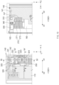
- FIG. 10 illustrates an electrical connection structure of the plurality of circuit boards according to an embodiment.
- FIG. 11 illustrates the electrical connection structure of the plurality of circuit boards according to an embodiment.
- FIG. 12 illustrates the electrical connection structure of the plurality of circuit boards according to an embodiment.
- the electronic device 100 may include the bracket 140, the plurality of circuit boards 210, and the plurality of rear cameras 320.
- the electronic device 100 may be configured such that the plurality of rear cameras 320 are electrically connected to the plurality of circuit boards 210.
- 1001 of FIG. 10 may be a view in which the third camera module (e.g., the third camera module 323 of FIG. 9 ) and the fourth camera module (e.g., the fourth camera module 231 of FIG. 9 ) are omitted from the electronic device 100 of FIG. 9 .
- 1002 of FIG. 10 may be a view in which the first camera structure 328 is omitted from the electronic device 100 in 1001 of FIG. 10 .
- the plurality of circuit boards 210 may include the first circuit board 220, the connecting circuit board 250, and the third circuit board 240.
- the first circuit board 220 may be understood as the main circuit board
- the third circuit board 240 may be understood as a sub-circuit board.
- a processor e.g., the processor 520 of FIG. 24
- the first circuit board 220 may be understood as the main circuit board
- the third circuit board 240 may be understood as a sub-circuit board.
- a processor e.g., the processor 520 of FIG. 24
- the first circuit board 220 may be connected with the first camera structure 328.
- the first connector C1 of the first camera structure 328 may be connected to the first circuit board 220.
- the first circuit board 220 may be connected with a flexible circuit board portion 273 of a slide circuit board (e.g., a slide circuit board 270 of FIG. 11 ).
- a fifth connector C5 of the flexible circuit board portion 273 may be connected to the first circuit board 220.
- the connecting circuit board 250 may be connected with the second circuit board 230 through the third connector C3, and an opposite end portion (e.g., an end portion facing the +Y-axis direction in FIG. 9 ) of the connecting circuit board 250 may be connected with the third circuit board 240 through the fourth connector C4. Accordingly, the connecting circuit board 250 may electrically connect the second circuit board 230 and the third circuit board 240. According to an embodiment, the connecting circuit board 250 may be electrically connected with the first circuit board 220 through the third circuit board 240.
- a structure for electrically connecting the first circuit board 220, the second circuit board 230, the third circuit board 240, and the connecting circuit board 250 is not limited to the illustrated embodiment, and various methods may be applied.
- the third circuit board 240 may be electrically connected with the second camera module 322.
- a sixth connector C6 of the second camera module 322 may be connected to the third circuit board 240.
- the third circuit board 240 may be electrically connected with the second camera module 322 through the sixth connector C6.
- the third circuit board 240 may be electrically connected with a side key module 195.
- a seventh connector C7 of the side key module 195 may be connected to the third circuit board 240.
- the third circuit board 240 may be electrically connected with the side key module 195 through the seventh connector C7.
- at least part of the side key module 195 may be disposed on a side surface (e.g., a side surface facing the +X-axis direction) of the bracket 140.
- the bracket 140 may have, in the side surface thereof, a key hole (not illustrated) in which at least part of the side key module 195 is accommodated.
- the key hole may penetrate at least part of the side surface of the bracket 140.
- the side key module 195 may be electrically connected with the first circuit board 220 through the third circuit board 240.
- the third circuit board 240 may electrically connect the connecting circuit board 250, the second camera module 322, and the side key module 195 with the first circuit board 220.
- the connecting circuit board 250 and the second camera module 322 may be connected to the third circuit board 240 and may be electrically connected with the first circuit board 220 through the third circuit board 240.
- the electronic device 100 according to an embodiment may be configured such that the second camera module 322, the side key module 195, and the connecting circuit board 250 are electrically connected with the first circuit board 220 through the third circuit board 240.
- the third circuit board 240 may overlap the third camera module 323 and the fourth camera module 324.
- FIG. 10 is a view in which the third camera module 323 and the fourth camera module 324 are omitted.
- the third circuit board 240 may overlap the third camera module 323 and the fourth camera module 324 and may be hidden by the third camera module 323 and the fourth camera module 324.
- the third circuit board 240 may be disposed under the third camera module 323 and the fourth camera module 324 (e.g., the +Z-axis direction).
- the plurality of rear cameras 320 may include the first camera module 321 and the second camera module 322. Although not illustrated in FIG. 10 , the plurality of rear cameras 320 may further include the third camera module (e.g., the third camera module 323 of FIG. 9 ) and the fourth camera module (e.g., the fourth camera module 324 of FIG. 9 ).
- the third camera module e.g., the third camera module 323 of FIG. 9
- the fourth camera module e.g., the fourth camera module 324 of FIG. 9 .
- the electronic device 100 may be configured such that the first camera module 321, the first sensor module 325, and the flash module 326 are formed to be an integrated module and are electrically connected with the first circuit board 220.
- the second camera module 322 may be connected to the third circuit board 240.
- the second camera module 322 may include the sixth connector C6 connected to the third circuit board 240.
- the second camera module 322 may be electrically connected with the third circuit board 240 through the sixth connector C6.
- the sixth connector C6 may extend from the second camera module 322 toward the third circuit board 240.
- the second camera module 322 may be electrically connected with the first circuit board 220 through the third circuit board 240.
- the first circuit board 220 and the second camera module 322 may transmit/receive electrical signals related to the second camera module 322 through the sixth connector C6 and the third circuit board 240.
- the electronic device 100 may include the bracket 140, the second structure 160, the front camera module 310, a second sensor module 340, a first speaker module 330, and the slide circuit board 270.
- 1101 of FIG. 11 may be a view in which the first circuit board 220, the third circuit board 240, the connecting circuit board 250, the third camera module 323, and the SIM socket 196 are omitted from the electronic device 100 in 1002 of FIG. 10 .
- 1102 of FIG. 11 may be a view in which the bracket 140 is omitted from the electronic device 100 in 1101 of FIG. 11 .
- 1101 of FIG. 11 illustrates the second surface 142 (e.g., the second surface 142 of FIG. 4 ) of the bracket 140
- 1102 of FIG. 11 illustrates the fourth surface 164b (e.g., the fourth surface 164b of FIG. 4 ) of the second structure 160.
- 1201 of FIG. 12 may be a view in which a cover 167 of the second structure 160 is omitted from the electronic device 100 in 1102 of FIG. 11 .
- 1202 of FIG. 12 may be a view in which the plate portion 164 of the second structure 160 is omitted from the electronic device 100 in 1201 of FIG. 12 .
- the slide circuit board 270 may be at least partially disposed on the second structure 160 to move together with the second structure 160.
- the slide circuit board 270 may include a fixed circuit board portion 271 fixedly disposed on the plate portion 164 of the second structure 160 and the flexible circuit board portion 273 extending from the fixed circuit board portion 271.
- the fixed circuit board portion 271 of the slide circuit board 270 may be fixedly disposed on the fourth surface 164b of the plate portion 164.
- the fixed circuit board portion 271 may move together with the second structure 160 when the second structure 160 moves relative to the bracket 140.
- the flexible circuit board portion 273 may flexibly extend from the fixed circuit board portion 271.
- the slide circuit board 270 may be configured such that the fixed circuit board portion 271 and the flexible circuit board portion 273 are integrally formed with each other.
- the slide circuit board 270 may be a rigid-flexible printed circuit board (RFPCB) including a rigid circuit board (e.g., the fixed circuit board portion 271) and a flexible circuit board (e.g., the flexible circuit board portion 273).
- RFPCB rigid-flexible printed circuit board
- the slide circuit board 270 may be configured such that the flexible circuit board portion 273 formed of an FPCB and the fixed circuit board portion 271 formed of a PCB are manufactured as separate components and connected with each other.
- the slide circuit board 270 may be electrically connected with the first circuit board 220.
- the slide circuit board 270 may be configured such that the flexible circuit board portion 273 is connected with the first circuit board 220 as illustrated in FIG. 10 .
- the slide circuit board 270 may be formed in a form in which the flexible circuit board portion 273 extends from the fixed circuit board portion 271 toward the first circuit board 220.
- the flexible circuit board portion 273 may include the fifth connector C5 connected to the first circuit board 220.
- the fifth connector C5 of the flexible circuit board portion 273 may be connected to the first circuit board 220, and accordingly the slide circuit board 270 may be electrically connected with the first circuit board 220 (refer to FIG. 10 ).
- the flexible circuit board portion 273 may pass through part of the bracket 140 in an up/down direction (e.g., the Z-axis direction) and may connect the fixed circuit board portion 271 and the first circuit board 220 facing each other with the bracket 140 therebetween.
- the first circuit board 220 may be located on the second surface 142 of the bracket 140
- the fixed circuit board portion 271 may be located between the fourth surface 164b of the second structure 160 and the first surface (e.g., the surface facing the +Z-axis direction) of the bracket 140.
- the bracket 140 may have an opening 147 formed through the bracket 140 in the up/down direction.
- the flexible circuit board portion 273 of the slide circuit board 270 may extend from the fixed circuit board portion 271 toward the second surface 142 of the bracket 140 through the opening 147.
- the flexible circuit board portion 273 may be configured such that at least part thereof penetrates the bracket 140 in the up/down direction through the opening 147 and opposite end portions are connected to the first circuit board 220 and the fixed circuit board portion 271.
- the flexible circuit board portion 273 may move in the direction parallel to the sliding directions D1 and D2 when the second structure 160 slides relative to the bracket 140.
- the flexible circuit board portion 273 may include one or more bending portion 273b and 273d such that at least part of the flexible circuit board portion 273 moves in the direction parallel to the sliding directions D1 and D2. The shape and motion of the flexible circuit board portion 273 will be described below in more detail with reference to FIG. 15 .
- the first speaker module 330 may be connected to the fixed circuit board portion 271 of the slide circuit board 270.
- the first speaker module 330 may include an eighth connector C8 connected to the fixed circuit board portion 271.
- the first speaker module 330 may be electrically connected with the slide circuit board 270 through the eighth connector C8.
- a ninth connector C9 to which the second sensor module 340 and the front camera module 310 are connected may be connected to the fixed circuit board portion 271 of the slide circuit board 270.
- the second sensor module 340 and the front camera module 310 may be electrically connected with the slide circuit board 270 through the ninth connector C9.
- a tenth connector C10 connected with the display circuit board 280 may be connected to the fixed circuit board portion 271 of the slide circuit board 270.
- opposite end portions of the tenth connector C10 may be connected to the display circuit board 280 and the fixed circuit board portion 271, and accordingly the tenth connector C10 may electrically connect the display circuit board 280 and the fixed circuit board portion 271.
- the display circuit board 280 may be electrically connected with a display (e.g., the display 170 of FIG. 3 ), and the display 170 may be electrically connected with the first circuit board 220 through the display circuit board 280 and the slide circuit board 270.
- the second structure 160 may include a module accommodation part 166 in which the front camera module 310, the second sensor module 340, and the first speaker module 330 are accommodated.
- the front camera module 310, the second sensor module 340, and the first speaker module 330 may be disposed inside the module accommodation part 166 of the second structure 160 and may move relative to the bracket 140 in the sliding directions D1 and D2 together with the second structure 160.
- the module accommodation part 166 may be formed on the plate portion 164 of the second structure 160.
- the module accommodation part 166 may be formed on the fourth surface 164b of the plate portion 164.
- the module accommodation part 166 may protrude to a predetermined height from the fourth surface 164b to surround the front camera module 310, the second sensor module 340, and the first speaker module 330.
- the cover 167 may be coupled to the module accommodation part 166 to cover the front camera module 310, the second sensor module 340, and the first speaker module 330.
- the cover 167 may be coupled to the top of the module accommodation part 166 (e.g., -Z-axis direction) and may overlap the front camera module 310, the second sensor module 340, and the first speaker module 330.
- the cover 167 may hide the front camera module 310, the second sensor module 340, and the first speaker module 330 such that the front camera module 310, the second sensor module 340, and the first speaker module 330 are not exposed on the fourth surface 164b of the second structure 160.
- the module accommodation part 166 and the cover 167 may be formed of a shielding member (e.g., a shield can) to shield electromagnetic waves.
- the slide circuit board 270 may include the fixed circuit board portion 271 fixedly disposed on the plate portion 164 of the second structure 160 and the flexible circuit board portion 273 that extends from the fixed circuit board portion 271 and that is electrically connected with the first circuit board 220.
- the fifth connector C5 of the flexible circuit board portion 273 may be connected to the first circuit board 220.
- the front camera module 310, the second sensor module 340, and the first speaker module 330 may be disposed in the module accommodation part 166 of the second structure 160.
- the module accommodation part 166 may overlap some of the plurality of rear cameras 320 in the first state and the second state.
- the module accommodation part 166 may move in the first direction D1 or the second direction D2 in the state in which at least part of the module accommodation part 166 overlaps the first camera module 321 in the Z-axis direction.
- a state in which some of the front camera module 310, the second sensor module 340, and the first speaker module 330 overlap the first camera module 321 may be formed as the second structure 160 moves.
- the plurality of rear cameras 320 may include the first camera structure 328, the second camera module 322, the third camera module 323, and the fourth camera module 324.
- the first camera structure 328 may include the first camera module 321, the first sensor module 325, and the flash module 326.
- the plurality of rear cameras 320 may be implemented with different types of camera modules.
- the first camera module 321 may be a time-of-flight (TOF) camera module.
- the first sensor module 325 disposed adjacent to the first camera module 321 may be a TOF transmitter TX for driving the TOF camera module.
- the second camera module 322 may be an ultra wide camera module.
- the third camera module 323 may be a wide camera module.
- the fourth camera module 324 may be a tele camera module.
- the types of the plurality of rear cameras 320 are not limited to the above-described examples, and various types of camera modules may be applied.
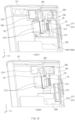
- FIG. 15 is a sectional view of part of the electronic device according to an embodiment.
- FIG. 16 is a sectional view of part of the electronic device according to an embodiment.
- FIG. 15 is a sectional view of the electronic device taken along line S3-S3' in FIG. 13 .
- FIG. 16 is a sectional view of the electronic device taken along line S4-S4' in FIG. 13 .
- the electronic device 100 may include the first structure 110 (e.g., the back cover 121 and the bracket 140), the second structure 160, the display 170, the display support member 193, the battery 192, the camera decoration member 124, the slide circuit board 270, the plurality of circuit boards 210, and the plurality of rear cameras (e.g., the second camera module 322 and the fourth camera module 324).
- the first structure 110 e.g., the back cover 121 and the bracket 140
- the second structure 160 e.g., the display 170, the display support member 193, the battery 192, the camera decoration member 124, the slide circuit board 270, the plurality of circuit boards 210, and the plurality of rear cameras.
- the components of the electronic device 100 illustrated in FIGS. 15 and 16 are identical or similar to some of the components of the electronic device 100 illustrated in FIGS. 1 to 14 , and repetitive descriptions will be omitted.
- the second structure 160 may be disposed over the first surface 141 of the bracket 140 (e.g., the +Z-axis direction).
- the second structure 160 may include the third surface 164a on which the display 170 is disposed and the fourth surface 164b facing the first surface 141 of the bracket 140.
- the fixed circuit board portion 271 of the slide circuit board 270 may be fixedly disposed on the fourth surface 164b of the second structure 160.
- the plurality of circuit boards 210 may include the first circuit board 220 and the third circuit board 240.
- the first circuit board 220 and the third circuit board 240 may be electrically connected with each other.
- the first circuit board 220 may be located between the bracket 140 and the back cover 121.
- the first circuit board 220 may be disposed on the second surface 142 of the bracket 140.
- the slide circuit board 270 and the third camera module 323 may be connected to the first circuit board 220.
- a connecting portion 275 e.g., the fifth connector C5 of FIGS. 10 to 12
- the slide circuit board 270 and the second connector C2 of the third camera module 323 may be connected to the first circuit board 220 (e.g., refer to FIGS. 9 and 13 ).
- the third circuit board 240 may be electrically connected with the first circuit board 220 through the eleventh connector C11.
- the eleventh connector C11 may extend from the third circuit board 240 and may be connected, between the first circuit board 220 and the bracket 140, to the first circuit board 220 (refer to 1402 of FIG. 14 ).
- the third circuit board 240 may be closer to the second surface 142 of the bracket 140 than the first circuit board 220.
- the first circuit board 220 may be located in a higher position with respect to the bracket 140 than the third circuit board 240.
- the slide circuit board 270 may include the fixed circuit board portion 271, the flexible circuit board portion 273, and the connecting portion 275 (e.g., the fifth connector C5).
- the connecting portion 275 may make contact with the first circuit board 220, and accordingly the slide circuit board 270 may be electrically connected with the first circuit board 220.
- the slide circuit board 270 may be configured such that at least some of the fixed circuit board portion 271, the flexible circuit board portion 273, and the connecting portion 275 are integrally formed.
- the structure of the slide circuit board 270 illustrated in FIG. 15 is illustrative, and the slide circuit board 270 is not limited thereto.
- the slide circuit board 270 may not include the connecting portion 275.
- the slide circuit board 270 may be configured such that the flexible circuit board portion 273 directly extends from, or is directly connected with, the first circuit board 220.
- the slide circuit board 270 may be integrally formed with part of the first circuit board 220.
- the connecting portion 275 may be fixed to the first circuit board 220, and the fixed circuit board portion 271 may be fixed to the second structure 160.
- the slide circuit board 270 may be configured such that the fixed circuit board portion 271 moves in the sliding directions D1 and D2 with respect to the relatively fixed connecting portion 275 when the second structure 160 moves in the sliding directions D1 and D2 relative to the bracket 140.
- the flexible circuit board portion 273 may be deformed in response to a movement of the fixed circuit board portion 271 in the state in which opposite end portions of the flexible circuit board portion 273 are connected to the fixed circuit board portion 271 and the connecting portion 275.
- the slide circuit board 270 may be deformed in a form in which the length of the first extending portion 273a is increased and the length of the second extending portion 273c is decreased.
- the slide circuit board 270 may be deformed in a form in which the length of the first extending portion 273a is decreased and the length of the second extending portion 273c is increased.
- the shape and motion of the flexible circuit board portion 273 are not limited to the above-described example.
- FIG. 17 is a sectional view of part of the electronic device according to an embodiment.
- 1701 of FIG. 17 is a sectional view of the electronic device taken along line S5-S5' in FIG. 13 .
- 1702 of FIG. 17 is a sectional view of the electronic device taken along line S6-S6' in FIG. 14 .
- the plurality of rear cameras 320 may include the first camera module 321, the second camera module 322, the third camera module 323, and the fourth camera module 324.
- the first camera module 321, the second camera module 322, the third camera module 323, and the fourth camera module 324 may be disposed in a row along the direction perpendicular to the sliding directions D1 and D2.
- the second structure 160 may include the third surface 164a on which the display 170 is disposed and the fourth surface 164b facing away from the third surface 164a.
- the module accommodation part 166 in which the front camera module 310 and the first speaker module 330 are accommodated, may be formed on the fourth surface 164b of the second structure 160.
- the module accommodation part 166 may have an empty space formed therein in which the front camera module 310 and the first speaker module 330 are accommodated.
- the second sensor module e.g., the second sensor module 340 of FIGS. 13 and 14
- the second sensor module may be accommodated together in the module accommodation part 166.
- the module accommodation part 166 may move while maintaining a state of overlapping the first camera module 321.
- the first camera module 321 may overlap the first speaker module 330, which is accommodated in the module accommodation part 166, in the Z-axis direction.
- the first camera module 321 may overlap the front camera module 310, which is accommodated in the module accommodation part 166, in the Z-axis direction.
- the electronic device 100 may be configured such that the first camera module 321 is disposed in a position overlapping the module accommodation part 166.
- the degree to which the plurality of rear cameras 320 (or, the camera decoration member 124) protrude from the rear side of the electronic device 100 may be reduced by locating the first camera module 321, which has a relatively small thickness among the plurality of rear cameras 320, over the module accommodation part 166 (e.g., the -Z-axis direction).
- the connecting portion 225 may connect the first circuit board layer 221 and the second circuit board layer 223.
- the connecting portion 225 may be disposed between the first circuit board layer 221 and the second circuit board layer 223 such that a shielded space 227 is formed between the first circuit board layer 221 and the second circuit board layer 223.
- various electric elements and/or electronic components may be disposed in the shielded space 227.
- a mounting rate of the first circuit board 220 may be improved as some electric elements or electronic components are disposed in the shielded space 227.
- the connecting portion 225 may include a plurality of VIAs (not illustrated) that electrically connect a conductive area of the first circuit board layer 221 and a conductive area of the second circuit board layer 223.
- the plurality of VIAs may pass through partial areas of the connecting portion 225 in a direction perpendicular to the circuit board layers 221 and 223.
- FIG. 19 illustrates the first state and the second state of the electronic device according to an embodiment.
- the electronic device 100 may include the rear case (e.g., the rear case 122 of FIG. 3 ), the side members 131 and 132, the guide members 152, and an antenna module 198.
- the rear case e.g., the rear case 122 of FIG. 3
- the side members 131 and 132 the guide members 152
- an antenna module 198 the antenna module 198.
- the antenna module 198 may be disposed to face the back cover 121.
- the back cover 121 may be disposed over the antenna module 198.
- the antenna module 198 may be configured to function as a rear antenna of the electronic device 100.
- at least part of the antenna module 198 may be surrounded by the rear case 122.
- the antenna module 198 may be disposed between the back cover 121 and the battery (e.g., the battery 192 of FIG. 3 ) (e.g., refer to FIG. 3 ).
- the antenna module 198 may include a near field communication (NFC) antenna, a wireless power consortium (WPC) antenna, a magnetic secure transmission (MST) antenna, and/or an ultra wide band (UWB) antenna.
- NFC near field communication
- WPC wireless power consortium
- MST magnetic secure transmission
- UWB ultra wide band
- the antenna module 198 may perform short-range communication with an external device, or may wirelessly transmit and receive electric power required for charging.
- an antenna structure may be formed by part of the second structure 160, a part of the side members 131 and 132, or a combination thereof.
- At least part of the second structure 160 may be configured to function as a side (e.g., an X-axis direction side) antenna of the electronic device 100.
- the conductive portions 163a, 163b, 163c, and 163d may operate as an antenna radiator for transmitting and receiving wireless signals in a specified band.
- the side members 131 and 132 may include the first side member 131 and the second side member 132, and at least parts of the first side member 131 and the second side member 132 may include conductive portions.
- the conductive portions of the first side member 131 and the second side member 132 may be formed of a metallic material.
- a method of using the side members 131 and 132 as antenna radiators may be substantially the same as the method of using the second structure 160 as an antenna radiator as described above.
- the conductive portions of the side members 131 and 132 may be electrically connected with wireless communication circuitry (e.g., the wireless communication module 592 of FIG. 24 ) of the electronic device 100 and may receive electric power from the wireless communication circuitry. Accordingly, the conductive portions of the side members 131 and 132 may operate as antenna radiators for transmitting and receiving wireless signals in specified bands.
- the first side member 131 and the second side member 132 may include cut-off portions P1, P2, P3, and P4 insulating the conductive portions.
- the second side member 132 may include the first cut-off portion P1 and the second cut-off portion P2.
- the second side member 132 may be configured such that some of the conductive portions separated by the first cut-off portion P1 and the second cut-off portion P2 operate as an antenna radiator or an antenna ground.
- the first side member 131 may include the third cut-off portion P3 and the fourth cut-off portion P4.
- the first side member 131 may be configured such that some of the conductive portions separated by the third cut-off portion P3 and the fourth cut-off portion P4 operate as an antenna radiator or an antenna ground.
- the side members 131 and 132 may be disposed to face at least parts of the guide members 151 and 152. Although not illustrated, the side members 131 and 132 may be coupled to edge portions (e.g., the edge portions 143 and 144 of FIG. 3 ) of the bracket 140 with the guide members 151 and 152 therebetween.
- the side members 131 and 132 may include connecting structures for electrical connections with the plurality of circuit boards 210 without interference by the guide members 151 and 152.
- the electrical connection structures of the side members 131 and 132 and the plurality of circuit boards 210 will be described below in more detail with reference to FIGS. 20 to 23 .
- FIG. 20 illustrates an electrical connection structure of the second side member and the plurality of circuit boards of the electronic device according to an embodiment.
- FIG. 21 illustrates the electrical connection structure of the second side member and the plurality of circuit boards of the electronic device according to an embodiment.
- FIGS. 20 and 21 may be views in which the second decoration member (e.g., the second decoration member 136 of FIG. 3 ) of the second side member (e.g., the second side member 132 of FIG. 3 ) is omitted.
- the second decoration member e.g., the second decoration member 136 of FIG. 3
- the second side member e.g., the second side member 132 of FIG. 3
- the electronic device 100 may include a connecting structure by which the second side cover 135 is electrically connected with a part (e.g., the second circuit board 230) of the plurality of circuit boards (e.g., the plurality of circuit boards 210 of FIG. 3 ).
- the electronic device 100 may include the bracket 140, the second side cover 135, the second guide member 152, and the second circuit board 230.
- the second circuit board 230 of the plurality of circuit boards 210 may be disposed on the bracket 140.
- the second circuit board 230 may be disposed on a partial area of the second surface 142 of the bracket 140.
- the second circuit board 230 may be disposed adjacent to the second edge portion 144 (e.g., the second edge portion 144 of FIG. 3 ) of the bracket 140 so as to be located in the lower end of the electronic device 100 (e.g., the -Y-axis direction).
- the second side cover 135 and the second guide member 152 may be fixedly coupled to the bracket 140.
- the second side cover 135 may be disposed to face the second edge portion 144 with the second guide member 152 therebetween.
- the second side cover 135 may include protruding portions 137 extending from partial areas of the second side cover 135 toward the second guide member 152 or the bracket 140.
- the protruding portions 137 may extend toward the second edge portion 144 of the bracket 140 to pass through partial areas of the second guide member 152.
- the protruding portions 137 may make electrical connection or contact with the second circuit board 230 such that a part of the conductive portions 135a, 135b, and 135c of the second side cover 135 operates as an antenna radiator.
- the protruding portions 137 may extend from at least a part of the conductive portions 135a, 135b, and 135c to have conductivity.
- the protruding portions 137 may include a first protruding portion 137a extending from the first conductive portion 135a, and a second protruding portion 137b and a third protruding portion 137c that extend from the second conductive portion 135b.
- the first protruding portion 137a may extend from one surface (e.g., a surface facing the +Y-axis direction) of the first conductive portion 135a toward the second edge portion 144 of the bracket 140.
- the second protruding portion 137b and the third protruding portion 137c may extend from one surface (e.g., a surface facing the +Y-axis direction) of the second conductive portion 135b toward the second edge portion 144 of the bracket 140.
- the second protruding portion 137b and the third protruding portion 137c may be spaced apart from each other at a predetermined interval.
- the protruding portions 137 may be electrically connected with the second circuit board 230 by making contact with the contact members 197.
- FIGS. 22 and 23 may be views in which the first decoration member (e.g., the first decoration member 134 of FIG. 3 ) of the first side member (e.g., the first side member 131 of FIG. 3 ) is omitted.
- first decoration member e.g., the first decoration member 134 of FIG. 3
- first side member e.g., the first side member 131 of FIG. 3
- the electronic device 100 may include a connecting structure by which the first side cover 133 is electrically connected with a part (e.g., the first circuit board 220) of the plurality of circuit boards (e.g., the plurality of circuit boards 210 of FIG. 3 ).
- the electronic device 100 may include the second structure 160, the first side cover 133, the first guide member 151, and the first circuit board 220.
- the first side cover 133 and the first guide member 151 may be fixedly coupled to the bracket (e.g., the bracket 140 of FIG. 3 ).
- the bracket 140 is not illustrated in FIGS. 22 and 23
- the first side cover 133 and the first guide member 151 may be coupled to the first edge portion (e.g., the first edge portion 143 of FIG. 3 ) of the bracket (e.g., the bracket 140 of FIG. 3 ) (e.g., refer to FIG. 10 ).
- the second side cover 135 may be disposed to face the second edge portion 144 with the second guide member 152 therebetween.
- the first circuit board 220 may be disposed on the second surface 142 of the bracket 140.
- the first side cover 133 may be configured to be electrically connected with the first circuit board 220 through a connecting member 199 disposed between the first side cover 133 and the first guide member 151.
- the first side cover 133 may include conductive portions 133a, 133b, and 133c in at least a portion thereof.
- the first side cover 133 may include the fourth conductive portion 133a, the fifth conductive portion 133b, and the sixth conductive portion 133c.
- the conductive portions 133a, 133b, and 133c may be formed of metal.
- the first side cover 133 may be configured such that at least a part of the conductive portions 133a, 133b, and 133c operates as an antenna radiator.
- a part of the fourth conductive portion 133a, the fifth conductive portion 133b, and the sixth conductive portion 133c may operate as an antenna radiator that receives electric power from wireless communication circuitry (e.g., the wireless communication module 592 of FIG. 24 ) and transmits and receives wireless signals in a specified band.
- wireless communication circuitry e.g., the wireless communication module 592 of FIG. 24
- the first side cover 133 may include the cut-off portions P3 and P4 insulating the conductive portions 133a, 133b, and 133c.
- the cut-off portions P3 and P4 may include the third cut-off portion P3 insulating the fourth conductive portion 133a and the fifth conductive portion 133b and the fourth cut-off portion P4 insulating the fifth conductive portion 133b and the sixth conductive portion 133c.
- the second side cover 135 may include a first contact area 1331 making contact with at least part of the connecting member 199.
- the first contact area 1331 may be formed on at least a partial area of the conductive portions 133a, 133b, and 133c.
- the first contact area 1331 may be formed on an inner surface (e.g., a surface facing the -Y-axis direction) of the first side cover 133 so as to face the first guide member 151.
- the first contact area 1331 may make contact with part (e.g., a second contact area 1991) of the connecting member 199.
- the conductive portions 133a, 133b, and 133c may be electrically connected with the connecting member 199 as the first contact area 1331 makes contact with the part of the connecting member 199.
- the first contact area 1331 may be formed on the fourth conductive portion 133a, but is not necessarily limited thereto.
- the connecting member 199 may extend from one surface of the first guide member 151 toward the first circuit board 220.
- the connecting member 199 may be disposed on an upper surface 151a of the first guide member 151 and may extend toward the first circuit board 220 through the first guide member 151.
- the first guide member 151 may have an opening (not illustrated) into which at least part of the connecting member 199 is inserted. The opening may penetrate at least part of the first guide member 151 in a direction (e.g., the Y-axis direction) perpendicular to the upper surface 151a.
- One portion of the connecting member 199 may be disposed between the first side cover 133 and the first guide member 151, and another portion of the connecting member 199 may pass through the first guide member 151 and may be connected with the first circuit board 220.
- the connecting member 199 may include the second contact area 1991 making contact with the first contact area 1331 of the first side cover 133.
- the second contact area 1991 and the first contact area 1331 may be arranged to face each other.
- the connecting member 199 may electrically connect the first side cover 133 and the first circuit board 220.
- the connecting member 199 may include an FPCB and an FRC.
- FIG. 24 is a block diagram of an electronic device in a network environment according to various embodiments.
- the electronic device 501 in the network environment 500 may communicate with an electronic device 502 via a first network 598 (e.g., a short-range wireless communication network), or at least one of an electronic device 504 or a server 508 via a second network 599 (e.g., a long-range wireless communication network).
- a first network 598 e.g., a short-range wireless communication network
- a second network 599 e.g., a long-range wireless communication network
- the electronic device 501 may communicate with the electronic device 504 via the server 508.
- the electronic device 501 may include a processor 520, memory 530, an input module 550, a sound output module 555, a display module 560, an audio module 570, a sensor module 576, an interface 577, a connecting terminal 578, a haptic module 579, a camera module 580, a power management module 588, a battery 589, a communication module 590, a subscriber identification module (SIM) 596, or an antenna module 597.
- at least one of the components e.g., the connecting terminal 578) may be omitted from the electronic device 501, or one or more other components may be added in the electronic device 501.
- some of the components e.g., the sensor module 576, the camera module 580, or the antenna module 597) may be implemented as a single component (e.g., the display module 560).
- the processor 520 may execute, for example, software (e.g., a program 540) to control at least one other component (e.g., a hardware or software component) of the electronic device 501 coupled with the processor 520, and may perform various data processing or computation. According to one embodiment, as at least part of the data processing or computation, the processor 520 may store a command or data received from another component (e.g., the sensor module 576 or the communication module 590) in volatile memory 532, process the command or the data stored in the volatile memory 532, and store resulting data in non-volatile memory 534.
- software e.g., a program 540
- the processor 520 may store a command or data received from another component (e.g., the sensor module 576 or the communication module 590) in volatile memory 532, process the command or the data stored in the volatile memory 532, and store resulting data in non-volatile memory 534.
- the processor 520 may include a main processor 521 (e.g., a central processing unit (CPU) or an application processor (AP)), or an auxiliary processor 523 (e.g., a graphics processing unit (GPU), a neural processing unit (NPU), an image signal processor (ISP), a sensor hub processor, or a communication processor (CP)) that is operable independently from, or in conjunction with, the main processor 521.
- a main processor 521 e.g., a central processing unit (CPU) or an application processor (AP)
- auxiliary processor 523 e.g., a graphics processing unit (GPU), a neural processing unit (NPU), an image signal processor (ISP), a sensor hub processor, or a communication processor (CP)
- the main processor 521 e.g., a central processing unit (CPU) or an application processor (AP)
- auxiliary processor 523 e.g., a graphics processing unit (GPU), a neural processing unit (NPU), an image signal processor
- the auxiliary processor 523 may include a hardware structure specified for artificial intelligence model processing.
- An artificial intelligence model may be generated by machine learning. Such learning may be performed, e.g., by the electronic device 501 where the artificial intelligence is performed or via a separate server (e.g., the server 508). Learning algorithms may include, but are not limited to, e.g., supervised learning, unsupervised learning, semi-supervised learning, or reinforcement learning.
- the artificial intelligence model may include a plurality of artificial neural network layers.
- the interface 577 may support one or more specified protocols to be used for the electronic device 501 to be coupled with the external electronic device (e.g., the electronic device 502) directly (e.g., wiredly) or wirelessly.
- the interface 577 may include, for example, a high definition multimedia interface (HDMI), a universal serial bus (USB) interface, a secure digital (SD) card interface, or an audio interface.
- HDMI high definition multimedia interface
- USB universal serial bus
- SD secure digital
- the wireless communication module 592 may support various technologies for securing performance on a high-frequency band, such as, e.g., beamforming, massive multiple-input and multiple-output (massive MIMO), full dimensional MIMO (FD-MIMO), array antenna, analog beam-forming, or large scale antenna.
- the wireless communication module 592 may support various requirements specified in the electronic device 501, an external electronic device (e.g., the electronic device 504), or a network system (e.g., the second network 599).
- commands or data may be transmitted or received between the electronic device 501 and the external electronic device 504 via the server 508 coupled with the second network 599.
- Each of the electronic devices 502 or 504 may be a device of a same type as, or a different type, from the electronic device 501.
- all or some of operations to be executed at the electronic device 501 may be executed at one or more of the external electronic devices 502, 504, or 508. For example, if the electronic device 501 should perform a function or a service automatically, or in response to a request from a user or another device, the electronic device 501, instead of, or in addition to, executing the function or the service, may request the one or more external electronic devices to perform at least part of the function or the service.
- the camera module 580 may include a lens assembly 610, a flash 620, an image sensor 630, an image stabilizer 640, memory 650 (e.g., buffer memory), or an image signal processor 660.
- the lens assembly 610 may collect light emitted or reflected from an object whose image is to be taken.
- the lens assembly 610 may include one or more lenses.
- the camera module 580 may include a plurality of lens assemblies 610. In such a case, the camera module 580 may form, for example, a dual camera, a 360-degree camera, or a spherical camera.
- the image sensor 630 may include one selected from image sensors having different attributes, such as a RGB sensor, a black-and-white (BW) sensor, an IR sensor, or a UV sensor, a plurality of image sensors having the same attribute, or a plurality of image sensors having different attributes.
- Each image sensor included in the image sensor 630 may be implemented using, for example, a charged coupled device (CCD) sensor or a complementary metal oxide semiconductor (CMOS) sensor.
- CCD charged coupled device
- CMOS complementary metal oxide semiconductor
- the image stabilizer 640 may move the image sensor 630 or at least one lens included in the lens assembly 610 in a particular direction, or control an operational attribute (e.g., adjust the read-out timing) of the image sensor 630 in response to the movement of the camera module 580 or the electronic device 501 including the camera module 580. This allows compensating for at least part of a negative effect (e.g., image blurring) by the movement on an image being captured.
- a negative effect e.g., image blurring
- the image stabilizer 640 may sense such a movement by the camera module 580 or the electronic device 501 using a gyro sensor (not shown) or an acceleration sensor (not shown) disposed inside or outside the camera module 580.
- the image stabilizer 640 may be implemented, for example, as an optical image stabilizer.
- the memory 650 may store, at least temporarily, at least part of an image obtained via the image sensor 630 for a subsequent image processing task.
- a raw image obtained e.g., a Bayer-patterned image, a high-resolution image
- its corresponding copy image e.g., a low-resolution image
- the memory 650 may be configured as at least part of the memory 530 or as a separate memory that is operated independently from the memory 530.
- the image signal processor 660 may perform one or more image processing with respect to an image obtained via the image sensor 630 or an image stored in the memory 650.
- the one or more image processing may include, for example, depth map generation, three-dimensional (3D) modeling, panorama generation, feature point extraction, image synthesizing, or image compensation (e.g., noise reduction, resolution adjustment, brightness adjustment, blurring, sharpening, or softening).
- the image signal processor 660 may perform control (e.g., exposure time control or read-out timing control) with respect to at least one (e.g., the image sensor 630) of the components included in the camera module 580.
- An image processed by the image signal processor 660 may be stored back in the memory 650for further processing, or may be provided to an external component (e.g., the memory 530, the display module 560, the electronic device 502, the electronic device 504, or the server 508) outside the camera module 580.
- the image signal processor 660 may be configured as at least part of the processor 520, or as a separate processor that is operated independently from the processor 520. If the image signal processor 660 is configured as a separate processor from the processor 520, at least one image processed by the image signal processor 660 may be displayed, by the processor 520, via the display module 560 as it is or after being further processed.
- the electronic device 501 may include a plurality of camera modules 580 having different attributes or functions.
- at least one of the plurality of camera modules 580 may form, for example, a wide-angle camera and at least another of the plurality of camera modules580 may forma telephoto camera.
- at least one of the plurality of camera modules 580 may form, for example, a front camera and at least another of the plurality of camera modules580 may forma rear camera.
- FIG. 26 is a block diagram illustrating the wireless communication module, the power management module, and the antenna module of the electronic device according to various embodiments.
- the wireless communication module 592 may include a magnetic secure transmission (MST) communication module 710 or a near-field communication (NFC) module 730, and the power management module 588 may include a wireless charging module 750.
- the antenna module 597 may include a plurality of antennas that include a MST antenna 797-1 connected with the MST communication module 710, a NFC antenna 797-3 connected with the NFC communication module 730, and a wireless charging antenna 797-5 connected with the wireless charging module 750.
- MST magnetic secure transmission
- NFC near-field communication
- the antenna module 597 may include a plurality of antennas that include a MST antenna 797-1 connected with the MST communication module 710, a NFC antenna 797-3 connected with the NFC communication module 730, and a wireless charging antenna 797-5 connected with the wireless charging module 750.
- the MST communication module 710 may receive a signal containing control information or payment information such as card information from the processor 520, generate a magnetic signal corresponding to the received signal, and then transfer the generated magnetic signal to the external electronic device 502 (e.g., a point-of-sale (POS) device) via the MST antenna 797-1.
- the MST communication module 710 may include a switching module (not shown) that includes one or more switches connected with the MST antenna 797-1, and control the switching module to change the direction of voltage or current supplied to the MST antenna 797-1 according to the received signal.
- the change of the direction of the voltage or current allows the direction of the magnetic signal (e.g., a magnetic field) emitted from the MST antenna 797-1 to change accordingly.
- the magnetic signal with its direction changing may cause an effect (e.g., a waveform) similar to that of a magnetic field that is generated when a magnetic card corresponding to the card information associated with the received signal is swiped through a card reader of the electronic device 502.
- payment-related information and a control signal that are received by the electronic device 502 in the form of the magnetic signal may be further transmitted to an external server 508 (e.g., a payment server) via the network 599.
- the NFC communication module 730 may obtain a signal containing control information or payment information such as card information from the processor 520 and transmit the obtained signal to the external electronic device 502 via the NFC antenna 797-3. According to an embodiment, the NFC communication module 730 may receive such a signal transmitted from the external electronic device 502 via the NFC antenna 797-3.
- the wireless charging module 750 may wirelessly transmit power to the external electronic device 502 (e.g., a cellular phone or wearable device) via the wireless charging antenna 797-5, or wirelessly receive power from the external electronic device 502 (e.g., a wireless charging device).
- the wireless charging module 750 may support one or more of various wireless charging schemes including, for example, a magnetic resonance scheme or a magnetic induction scheme.
- the MST antenna 797-1, the NFC antenna 797-3, or the wireless charging antenna 797-5 may share at least part of their radiators.
- the radiator of the MST antenna 797-1 may be used as the radiator of the NFC antenna 797-3 or the wireless charging antenna 797-5, or vice versa.
- the antenna module 597 may include a switching circuit (not shown) adapted to selectively connect (e.g., close) or disconnect (e.g.
- the NFC communication module 730 or the wireless charging module 750 may control the switching circuit to temporarily disconnect at least one portion of the radiators shared by the NFC antenna 797-3 and the wireless charging antenna 797-5 from the NFC antenna 797-3 and to connect the at least one portion of the radiators with the wireless charging antenna 797-5.
- At least one function of the MST communication module 710, the NFC communication module 730, or the wireless charging module 750 may be controlled by an external processor (e.g., the processor 520).
- at least one specified function (e.g., a payment function) of the MST communication module 710 or the NFC communication module 730 may be performed in a trusted execution environment (TEE).
- the TEE may form an execution environment in which, for example, at least some designated area of the memory 530 is allocated to be used for performing a function (e.g., a financial transaction or personal information-related function) that requires a relatively high level of security. In such a case, access to the at least some designated area of the memory 530may be restrictively permitted, for example, according to an entity accessing thereto or an application being executed in the TEE.
- the first structure may include a rear member 120 that forms a rear side of the electronic device, a bracket 140 that is disposed between the rear member and the second structure and that supports the plurality of circuit boards, a side member 130 that forms a lateral side of the electronic device and that is located on opposite sides of the rear member, and a guide member 150 disposed between the bracket and the side member and connected to opposite end portions of the display support member.
- the guide member includes guide grooves 1521 in which the opposite end portions of the display support member are accommodated, and the guide member is configured to guide a movement of the display support member. At least part of the side member may pass through the guide member and may make contact with a contact member 197 disposed on at least a part of the plurality of circuit boards, such that the side member is electrically connected to the plurality of circuit boards.
- the side member may include a first side member 131 that is located at one end of the rear member and that forms a first lateral side of the electronic device and a second side member 132 that is located at an opposite end of the rear member and that forms a second lateral side of the electronic device.
- the guide member may include a first guide member 151 disposed between a first edge portion 143 of the bracket and the first side member and a second guide member 152 disposed between a second edge portion 144 of the bracket and the second side member.
- the first lateral side and the second lateral side of the electronic device may be lateral sides that face a direction perpendicular to the sliding direction.
Landscapes
- Engineering & Computer Science (AREA)
- Theoretical Computer Science (AREA)
- Computer Hardware Design (AREA)
- Signal Processing (AREA)
- Physics & Mathematics (AREA)
- General Physics & Mathematics (AREA)
- General Engineering & Computer Science (AREA)
- Human Computer Interaction (AREA)
- Mathematical Physics (AREA)
- Telephone Set Structure (AREA)
- Devices For Indicating Variable Information By Combining Individual Elements (AREA)
Claims (15)
- Dispositif électronique (100) comprenant :une première structure (110) ;une seconde structure (160) couplée à la première structure (110) pour se déplacer par rapport à celle-ci dans une première direction ou une seconde direction opposée à la première direction ;un écran (170) conçu de sorte qu'une zone partielle est disposée sur la seconde structure (160) pour se déplacer conjointement avec la seconde structure (160) et qu'au moins une partie d'une zone restante est située à l'intérieur de la première structure (110), dans lequel une taille d'une zone de l'écran (170) conçue pour former un côté avant du dispositif électronique (100) est modifiée lorsque la seconde structure (160) se déplace ;un élément de support d'écran (193) fixé à au moins une partie d'une surface arrière de l'écran (170) pour supporter l'écran (170) conjointement avec la seconde structure (160) et comprenant une première partie d'extrémité et une seconde partie d'extrémité ; etune pluralité de cartes de circuit (210) disposées à l'intérieur de la première structure (110), la pluralité de cartes de circuit (210) comprenant au moins une carte de circuit imprimé,dans lequel la première structure (110) comprend :un premier élément latéral (131) et un second élément latéral (132) conçus pour former des côtés latéraux du dispositif électronique (100) ; etun premier élément de guidage (151) et un second élément de guidage (152) conçus pour guider un mouvement de l'élément de support d'écran (193),dans lequel le premier élément de guidage (151) et le second élément de guidage (152) comprennent des rainures de guidage (1521) où la première partie d'extrémité et la seconde partie d'extrémité de l'élément de support d'écran (193) sont reçues, etdans lequel au moins une partie du second élément latéral (132) traverse le second élément de guidage (152) et établit un contact avec un élément de contact (197) disposé sur au moins une partie de la pluralité de cartes de circuit (210), de sorte que le second élément latéral (132) est relié électriquement à la pluralité de cartes de circuit (210).
- Dispositif électronique (100) de la revendication 1, dans lequel la première structure (110) comprend en outre un élément arrière (120) conçu pour former un côté arrière du dispositif électronique (100) et une patte (140) disposée entre l'élément arrière (120) et la seconde structure (160) et conçue pour supporter la pluralité de cartes de circuit (210), dans lequel le premier élément latéral (131) est situé au niveau d'une première extrémité de l'élément arrière (120) et conçu pour former un premier côté latéral du dispositif électronique (100) et le second élément latéral (132) est situé au niveau d'une seconde extrémité de l'élément arrière (120) et conçu pour former un second côté latéral du dispositif électronique (100),dans lequel le premier élément de guidage (151) est disposé entre une première partie de bord (143) de la patte (140) et le premier élément latéral (131), et le second élément de guidage (152) est disposé entre une seconde partie de bord (144) de la patte (140) et le second élément latéral (132), etdans lequel le premier côté latéral et le second côté latéral du dispositif électronique (100) sont des côtés latéraux conçus pour faire face à une direction perpendiculaire à une direction de coulissement.
- Dispositif électronique (100) de la revendication 2, dans lequel le premier élément latéral (131) et le premier élément de guidage (151) sont couplés de manière fixe à la première partie de bord (143) de la patte (140), et
dans lequel le second élément latéral (132) et le second élément de guidage (152) sont couplés de manière fixe à la seconde partie de bord (144) de la patte (140). - Dispositif électronique (100) de la revendication 2, dans lequel le second élément latéral (132) comprend une partie saillante (137) conçue pour s'étendre depuis une zone partielle du second élément latéral (132) vers le second élément de guidage (152), et
dans lequel le second élément de guidage (152) comprend un évidement (153, 154) où au moins une partie de la partie saillante (137) est disposée. - Dispositif électronique (100) de la revendication 4, dans lequel la partie saillante (137) traverse une partie du second élément de guidage (152) à travers l'évidement (153, 154) et établit un contact avec l'élément de contact (197), de sorte que le second élément latéral (132) est relié électriquement à la pluralité de cartes de circuit (210) à travers l'élément de contact pour utiliser le second élément latéral comme un élément rayonnant d'antenne.
- Dispositif électronique de la revendication 4, dans lequel le second élément latéral (132) comprend une pluralité de parties conductrices (135a, 135b, 135c),dans lequel la pluralité de parties conductrices (135a, 135b, 135c) comprennent une première partie conductrice (135a) et une deuxième partie conductrice (135b) espacées de la première partie conductrice (135a), etdans lequel la partie saillante (137) comprend une première partie saillante (137a) conçue pour s'étendre à partir de la première partie conductrice (135a) et une deuxième partie saillante (137b) conçue pour s'étendre à partir de la deuxième partie conductrice (135b).
- Dispositif électronique (100) de la revendication 6, dans lequel l'élément de contact (197) comprend un premier élément de contact (197a) conçu pour établir un contact avec la première partie saillante (137a) et un deuxième élément de contact (197b) conçu pour établir un contact avec la deuxième partie saillante (137b).
- Dispositif électronique (100) de la revendication 7, dans lequel la partie saillante (137) comprend en outre une troisième partie saillante (137c) conçue pour s'étendre depuis la deuxième partie conductrice (135b), et
dans lequel la deuxième partie saillante (137b) et la troisième partie saillante (137c) sont espacées l'une de l'autre par un espace prédéterminé dans la direction de coulissement. - Dispositif électronique (100) de la revendication 8, dans lequel l'évidement (153, 154) comprend un premier évidement (153) correspondant à la première partie saillante (137a) et à la deuxième partie saillante (137b) et un second évidement (154) correspondant à la troisième partie saillante (137c), et
dans lequel l'élément de contact (197) comprend en outre un troisième élément de contact (197c) conçu pour établir un contact avec la troisième partie saillante (137c). - Dispositif électronique (100) de la revendication 6, dans lequel la pluralité de parties conductrices (135a, 135b, 135c) comprennent en outre une troisième partie conductrice (135c) espacée de la deuxième partie conductrice (135b),dans lequel le second élément latéral (132) comprend une première partie de coupure (P1) disposée entre la première partie conductrice (135a) et la deuxième partie conductrice (135b) et une deuxième partie de coupure (P2) disposée entre la deuxième partie conductrice (135b) et la troisième partie conductrice (135c), etdans lequel au moins l'une de la première partie conductrice (135a), de la deuxième partie conductrice (135b) ou de la troisième partie conductrice (135c) est reliée électriquement à un circuit de communication sans fil disposé sur au moins une partie de la pluralité de cartes de circuit (210) et fonctionne comme un élément rayonnant d'antenne ou une masse d'antenne.
- Dispositif électronique (100) de la revendication 1, dans lequel l'élément de contact (197) est relié électriquement à la pluralité de cartes de circuit (210) et comprend au moins l'un d'un clip C ou d'une goupille pogo.
- Dispositif électronique (100) de la revendication 2, comprenant en outre :un élément de liaison (199) conçu pour relier électriquement le premier élément latéral (131) et la pluralité de cartes de circuit (210),dans lequel l'élément de liaison (199) traverse au moins une partie du premier élément de guidage (151) dans une direction perpendiculaire au premier côté latéral de sorte qu'une zone partielle est disposée entre le premier élément latéral (131) et le premier élément de guidage (151) et qu'une autre zone partielle est reliée à la pluralité de cartes de circuit (210).
- Dispositif électronique (100) de la revendication 12, dans lequel le premier élément latéral (131) comprend, sur une surface conçue pour faire face au premier élément de guidage (151), une première zone de contact (1331) conçue pour établir un contact avec l'élément de liaison (199),dans lequel une seconde zone de contact (1991) conçue pour établir un contact avec la première zone de contact (1331) est formée sur l'une zone partielle de l'élément de liaison (199), etdans lequel le premier élément latéral (131) et l'élément de liaison (199) sont reliés électriquement par contact entre la première zone de contact (1331) et la seconde zone de contact (1991).
- Dispositif électronique (100) de la revendication 13, dans lequel le premier élément latéral (131) comprend une partie conductrice (133a, 133b, 133c) sur au moins une partie de celuici, et
dans lequel la première zone de contact (1331) est formée sur une partie de la partie conductrice (133a, 133b, 133c). - Dispositif électronique (100) de la revendication 14, dans lequel la partie conductrice (133a, 133b, 133c) du premier élément latéral (131) comprend une quatrième partie conductrice (133a), une cinquième partie conductrice (133b) espacée de la quatrième partie conductrice (133a), et une sixième partie conductrice (133c) espacée de la cinquième partie conductrice (133b),dans lequel le premier élément latéral (131) comprend une troisième partie de coupure disposée entre la quatrième partie conductrice (133a) et la cinquième partie conductrice (133b) et une quatrième partie de coupure disposée entre la cinquième partie conductrice (133b) et la sixième partie conductrice (133c), etdans lequel au moins l'une de la quatrième partie conductrice (133a), de la cinquième partie conductrice (133b) ou de la sixième partie conductrice (133c) est reliée électriquement à un circuit de communication sans fil disposé sur au moins une partie de la pluralité de cartes de circuit (210) et fonctionne comme un élément rayonnant d'antenne ou une masse d'antenne.
Applications Claiming Priority (3)
| Application Number | Priority Date | Filing Date | Title |
|---|---|---|---|
| KR20200086553 | 2020-07-14 | ||
| KR1020210070800A KR20220008751A (ko) | 2020-07-14 | 2021-06-01 | 플렉서블 디스플레이를 포함하는 전자 장치 |
| PCT/KR2021/008962 WO2022015011A1 (fr) | 2020-07-14 | 2021-07-13 | Appareil électronique comprenant un écran souple |
Publications (4)
| Publication Number | Publication Date |
|---|---|
| EP4167050A1 EP4167050A1 (fr) | 2023-04-19 |
| EP4167050A4 EP4167050A4 (fr) | 2023-12-20 |
| EP4167050C0 EP4167050C0 (fr) | 2025-04-16 |
| EP4167050B1 true EP4167050B1 (fr) | 2025-04-16 |
Family
ID=79555588
Family Applications (1)
| Application Number | Title | Priority Date | Filing Date |
|---|---|---|---|
| EP21842226.9A Active EP4167050B1 (fr) | 2020-07-14 | 2021-07-13 | Appareil électronique comprenant un écran souple |
Country Status (4)
| Country | Link |
|---|---|
| US (1) | US12120256B2 (fr) |
| EP (1) | EP4167050B1 (fr) |
| CN (1) | CN116134408A (fr) |
| WO (1) | WO2022015011A1 (fr) |
Families Citing this family (4)
| Publication number | Priority date | Publication date | Assignee | Title |
|---|---|---|---|---|
| US12166911B2 (en) * | 2021-03-02 | 2024-12-10 | Apple Inc. | Handheld electronic device |
| CN113411427B (zh) * | 2021-06-25 | 2024-02-27 | 维沃移动通信有限公司 | 电子设备 |
| CN119497309B (zh) * | 2023-08-14 | 2026-04-17 | 北京小米移动软件有限公司 | 电子设备 |
| WO2026014860A1 (fr) * | 2024-07-08 | 2026-01-15 | 삼성전자주식회사 | Dispositif pouvant être porté sur soi comprenant une antenne |
Family Cites Families (43)
| Publication number | Priority date | Publication date | Assignee | Title |
|---|---|---|---|---|
| BRPI0507769A (pt) | 2004-02-10 | 2007-09-04 | Lee Han Sang | mecanismo de movimemnto e instrumento integrado com o mesmo |
| KR100624018B1 (ko) | 2004-02-10 | 2006-09-18 | 한 상 이 | 슬라이드 방식 휴대폰용 슬라이딩 장치 |
| US8199471B2 (en) | 2004-10-05 | 2012-06-12 | Creator Technology B.V. | Rollable display device |
| JP5039855B2 (ja) | 2008-09-05 | 2012-10-03 | アップル インコーポレイテッド | ハンドヘルド演算装置 |
| US7697281B2 (en) | 2008-09-05 | 2010-04-13 | Apple Inc. | Handheld computing device |
| US8126170B2 (en) | 2008-09-05 | 2012-02-28 | Apple Inc. | Electromagnetic interference shields with piezos |
| KR101153373B1 (ko) | 2010-10-20 | 2012-06-07 | (주) 프렉코 | 휴대 단말기용 슬라이드-틸트 힌지장치 |
| CN102123187B (zh) | 2011-03-15 | 2014-08-27 | 叶尔肯·拜山 | 伸缩式手机 |
| KR101863924B1 (ko) | 2011-06-21 | 2018-06-01 | 엘지전자 주식회사 | 이동 단말기 |
| US8711566B2 (en) | 2011-09-02 | 2014-04-29 | Microsoft Corporation | Expandable mobile device |
| US8825122B2 (en) | 2011-09-21 | 2014-09-02 | Htc Corporation | Hand-held deivce |
| KR20150105717A (ko) | 2014-03-10 | 2015-09-18 | (주)드림텍 | 모바일 기기의 카메라 모듈 구조 |
| US9521321B1 (en) | 2015-02-11 | 2016-12-13 | 360 Lab Llc. | Enabling manually triggered multiple field of view image capture within a surround image mode for multi-lens mobile devices |
| KR101792692B1 (ko) | 2015-08-28 | 2017-11-01 | 이유구 | 롤러블 디스플레이를 갖는 휴대용 단말기 |
| KR101733497B1 (ko) | 2015-09-24 | 2017-05-24 | 엘지전자 주식회사 | 이동 단말기 |
| CN106790792B (zh) | 2016-12-08 | 2019-02-05 | Oppo广东移动通信有限公司 | 成像模组及移动终端 |
| JP2020504869A (ja) * | 2016-12-29 | 2020-02-13 | シェンジェン ロイオル テクノロジーズ カンパニー リミテッドShenzhen Royole Technologies Co., Ltd. | フレキシブル電子装置 |
| KR102643660B1 (ko) | 2017-02-14 | 2024-03-06 | 삼성전자주식회사 | 생체 센서를 포함하는 전자 장치 |
| US10996713B2 (en) | 2017-08-07 | 2021-05-04 | Apple Inc. | Portable electronic device |
| US11158929B2 (en) * | 2017-09-29 | 2021-10-26 | Futurewei Technologies, Inc. | Antenna placement arrangements on device with extendable display |
| KR102620508B1 (ko) | 2017-11-24 | 2024-01-03 | 삼성전자주식회사 | 가요성 기판과 도전층 사이에 응력 완화 층을 갖는 디스플레이 모듈을 포함하는 전자 장치 |
| KR102408112B1 (ko) | 2018-01-12 | 2022-06-13 | 삼성전자주식회사 | 플렉서블 디스플레이를 포함하는 전자 장치 및 그것에 적용되는 전자 부품 배치 구조 |
| KR102410217B1 (ko) | 2018-02-08 | 2022-06-17 | 엘지전자 주식회사 | 이동 단말기 |
| CN207910858U (zh) | 2018-02-09 | 2018-09-25 | 广东欧珀移动通信有限公司 | 手机 |
| KR102266152B1 (ko) | 2018-02-22 | 2021-06-17 | 삼성전자주식회사 | 디스플레이 영역의 크기 변경이 가능한 플렉시블 디스플레이를 포함하는 전자 장치 및 그 제어 방법 |
| KR102269604B1 (ko) | 2018-02-23 | 2021-06-28 | 삼성전자주식회사 | 이동 가능한 플렉서블 디스플레이를 포함하는 전자 장치 |
| KR102255469B1 (ko) | 2018-03-06 | 2021-05-24 | 삼성전자주식회사 | 플렉서블한 디스플레이를 포함하는 전자 장치 및 그 동작 방법 |
| KR102460471B1 (ko) | 2018-03-27 | 2022-10-28 | 삼성전자주식회사 | 이동 가능한 플렉서블 디스플레이를 포함하는 전자 장치 및 그 동작 방법 |
| KR102481292B1 (ko) | 2018-04-13 | 2022-12-26 | 삼성전자주식회사 | 플렉시블 디스플레이를 포함하는 전자 장치 |
| KR102486663B1 (ko) | 2018-06-19 | 2023-01-11 | 삼성전자 주식회사 | 플렉서블 디스플레이 및 안테나를 포함하는 전자 장치 |
| KR102468068B1 (ko) | 2018-07-13 | 2022-11-16 | 엘지디스플레이 주식회사 | 플렉서블 디스플레이 장치 |
| TWI675235B (zh) | 2018-10-11 | 2019-10-21 | 友達光電股份有限公司 | 顯示裝置 |
| KR102624049B1 (ko) | 2018-11-05 | 2024-01-12 | 삼성전자주식회사 | 안테나를 포함하는 전자 장치 |
| KR102548573B1 (ko) | 2018-11-06 | 2023-06-28 | 삼성전자 주식회사 | 안테나, 안테나와 적어도 일부 중첩하여 배치되는 유전체를 포함하는 전자 장치 |
| KR102106296B1 (ko) | 2018-11-29 | 2020-05-04 | 삼성전자주식회사 | 카메라를 포함하는 전자 장치 및 그것의 동작 방법 |
| KR102180676B1 (ko) | 2018-12-28 | 2020-11-20 | 주식회사 다이아벨 | 전자기기용 슬라이딩 장치 |
| WO2021045262A1 (fr) | 2019-09-05 | 2021-03-11 | 엘지전자 주식회사 | Terminal mobile |
| US11997223B2 (en) * | 2019-12-12 | 2024-05-28 | Lg Electronics Inc. | Mobile terminal |
| WO2021132744A1 (fr) | 2019-12-23 | 2021-07-01 | 엘지전자 주식회사 | Terminal mobile |
| EP4096201B1 (fr) * | 2020-01-20 | 2025-07-23 | LG Electronics Inc. | Terminal mobile |
| WO2021162139A1 (fr) * | 2020-02-11 | 2021-08-19 | 엘지전자 주식회사 | Terminal mobile |
| CN111243440B (zh) | 2020-03-11 | 2022-05-17 | 昆山国显光电有限公司 | 一种柔性显示装置 |
| WO2021187641A1 (fr) | 2020-03-19 | 2021-09-23 | 엘지전자 주식회사 | Terminal mobile |
-
2021
- 2021-07-13 EP EP21842226.9A patent/EP4167050B1/fr active Active
- 2021-07-13 CN CN202180060618.5A patent/CN116134408A/zh active Pending
- 2021-07-13 WO PCT/KR2021/008962 patent/WO2022015011A1/fr not_active Ceased
-
2023
- 2023-01-03 US US18/149,483 patent/US12120256B2/en active Active
Also Published As
| Publication number | Publication date |
|---|---|
| EP4167050A1 (fr) | 2023-04-19 |
| US12120256B2 (en) | 2024-10-15 |
| CN116134408A (zh) | 2023-05-16 |
| EP4167050C0 (fr) | 2025-04-16 |
| US20230156104A1 (en) | 2023-05-18 |
| WO2022015011A1 (fr) | 2022-01-20 |
| EP4167050A4 (fr) | 2023-12-20 |
Similar Documents
| Publication | Publication Date | Title |
|---|---|---|
| EP4163760B1 (fr) | Dispositif électronique comprenant un écran souple | |
| EP4167050B1 (fr) | Appareil électronique comprenant un écran souple | |
| US11463607B2 (en) | Camera module and electronic device including the same | |
| KR20220008751A (ko) | 플렉서블 디스플레이를 포함하는 전자 장치 | |
| EP4170454B1 (fr) | Dispositif électronique comprenant un écran souple | |
| US12399377B2 (en) | Camera module including image stabilization assembly and electronic device including the camera module | |
| US20250048571A1 (en) | Electronic device comprising hinge structure for folding display | |
| US12142071B2 (en) | Electronic device including fingerprint sensor | |
| EP4471536A1 (fr) | Dispositif électronique comprenant un écran | |
| US20240414254A1 (en) | Electronic device for controlling that size of exposure area of flexible display corresponds to ratio of content display area, and control method therefor | |
| US20250274665A1 (en) | Method of providing preview image and electronic device therefor | |
| US20250168269A1 (en) | Electronic device for reconstructing background image | |
| KR102870349B1 (ko) | 카메라 모듈을 포함하는 전자 장치 | |
| US20250008011A1 (en) | Electronic apparatus including antenna | |
| US20250039525A1 (en) | Camera module and electronic device including the same | |
| US12498765B2 (en) | Method for displaying preview image and electronic device supporting the same | |
| US11974036B2 (en) | Electronic device including flexible display and camera | |
| EP4310588A1 (fr) | Stabilisateur d'image et dispositif électronique le comprenant | |
| KR20220031345A (ko) | 카메라를 포함하는 전자 장치 | |
| EP4510380A1 (fr) | Antenne et dispositif électronique comprenant une antenne | |
| EP4611383A1 (fr) | Dispositif électronique comprenant un module de caméra | |
| US20250023970A1 (en) | Electronic device comprising antenna member | |
| US20250338404A1 (en) | Camera module with improved degree of design freedom, and electronic device comprising same | |
| KR102929703B1 (ko) | 전자 장치 및 전자 장치의 지문 정보 획득 방법 | |
| US20240184379A1 (en) | Electronic apparatus for detecting motion gesture, and operation method therefor |
Legal Events
| Date | Code | Title | Description |
|---|---|---|---|
| STAA | Information on the status of an ep patent application or granted ep patent |
Free format text: STATUS: THE INTERNATIONAL PUBLICATION HAS BEEN MADE |
|
| PUAI | Public reference made under article 153(3) epc to a published international application that has entered the european phase |
Free format text: ORIGINAL CODE: 0009012 |
|
| STAA | Information on the status of an ep patent application or granted ep patent |
Free format text: STATUS: REQUEST FOR EXAMINATION WAS MADE |
|
| 17P | Request for examination filed |
Effective date: 20230111 |
|
| AK | Designated contracting states |
Kind code of ref document: A1 Designated state(s): AL AT BE BG CH CY CZ DE DK EE ES FI FR GB GR HR HU IE IS IT LI LT LU LV MC MK MT NL NO PL PT RO RS SE SI SK SM TR |
|
| DAV | Request for validation of the european patent (deleted) | ||
| DAX | Request for extension of the european patent (deleted) | ||
| A4 | Supplementary search report drawn up and despatched |
Effective date: 20231122 |
|
| RIC1 | Information provided on ipc code assigned before grant |
Ipc: G09F 9/30 20060101ALI20231116BHEP Ipc: H04M 1/02 20060101ALI20231116BHEP Ipc: G06F 1/16 20060101AFI20231116BHEP |
|
| GRAP | Despatch of communication of intention to grant a patent |
Free format text: ORIGINAL CODE: EPIDOSNIGR1 |
|
| STAA | Information on the status of an ep patent application or granted ep patent |
Free format text: STATUS: GRANT OF PATENT IS INTENDED |
|
| INTG | Intention to grant announced |
Effective date: 20241111 |
|
| GRAS | Grant fee paid |
Free format text: ORIGINAL CODE: EPIDOSNIGR3 |
|
| GRAA | (expected) grant |
Free format text: ORIGINAL CODE: 0009210 |
|
| STAA | Information on the status of an ep patent application or granted ep patent |
Free format text: STATUS: THE PATENT HAS BEEN GRANTED |
|
| AK | Designated contracting states |
Kind code of ref document: B1 Designated state(s): AL AT BE BG CH CY CZ DE DK EE ES FI FR GB GR HR HU IE IS IT LI LT LU LV MC MK MT NL NO PL PT RO RS SE SI SK SM TR |
|
| REG | Reference to a national code |
Ref country code: GB Ref legal event code: FG4D |
|
| REG | Reference to a national code |
Ref country code: CH Ref legal event code: EP Ref country code: DE Ref legal event code: R096 Ref document number: 602021029359 Country of ref document: DE |
|
| REG | Reference to a national code |
Ref country code: IE Ref legal event code: FG4D |
|
| U01 | Request for unitary effect filed |
Effective date: 20250507 |
|
| U07 | Unitary effect registered |
Designated state(s): AT BE BG DE DK EE FI FR IT LT LU LV MT NL PT RO SE SI Effective date: 20250514 |
|
| PGFP | Annual fee paid to national office [announced via postgrant information from national office to epo] |
Ref country code: GB Payment date: 20250624 Year of fee payment: 5 |
|
| U20 | Renewal fee for the european patent with unitary effect paid |
Year of fee payment: 5 Effective date: 20250723 |
|
| PG25 | Lapsed in a contracting state [announced via postgrant information from national office to epo] |
Ref country code: ES Free format text: LAPSE BECAUSE OF FAILURE TO SUBMIT A TRANSLATION OF THE DESCRIPTION OR TO PAY THE FEE WITHIN THE PRESCRIBED TIME-LIMIT Effective date: 20250416 |
|
| PG25 | Lapsed in a contracting state [announced via postgrant information from national office to epo] |
Ref country code: GR Free format text: LAPSE BECAUSE OF FAILURE TO SUBMIT A TRANSLATION OF THE DESCRIPTION OR TO PAY THE FEE WITHIN THE PRESCRIBED TIME-LIMIT Effective date: 20250717 Ref country code: NO Free format text: LAPSE BECAUSE OF FAILURE TO SUBMIT A TRANSLATION OF THE DESCRIPTION OR TO PAY THE FEE WITHIN THE PRESCRIBED TIME-LIMIT Effective date: 20250716 |
|
| PG25 | Lapsed in a contracting state [announced via postgrant information from national office to epo] |
Ref country code: PL Free format text: LAPSE BECAUSE OF FAILURE TO SUBMIT A TRANSLATION OF THE DESCRIPTION OR TO PAY THE FEE WITHIN THE PRESCRIBED TIME-LIMIT Effective date: 20250416 |
|
| PG25 | Lapsed in a contracting state [announced via postgrant information from national office to epo] |
Ref country code: HR Free format text: LAPSE BECAUSE OF FAILURE TO SUBMIT A TRANSLATION OF THE DESCRIPTION OR TO PAY THE FEE WITHIN THE PRESCRIBED TIME-LIMIT Effective date: 20250416 |
|
| PG25 | Lapsed in a contracting state [announced via postgrant information from national office to epo] |
Ref country code: RS Free format text: LAPSE BECAUSE OF FAILURE TO SUBMIT A TRANSLATION OF THE DESCRIPTION OR TO PAY THE FEE WITHIN THE PRESCRIBED TIME-LIMIT Effective date: 20250716 |
|
| PG25 | Lapsed in a contracting state [announced via postgrant information from national office to epo] |
Ref country code: IS Free format text: LAPSE BECAUSE OF FAILURE TO SUBMIT A TRANSLATION OF THE DESCRIPTION OR TO PAY THE FEE WITHIN THE PRESCRIBED TIME-LIMIT Effective date: 20250816 |
|
| PG25 | Lapsed in a contracting state [announced via postgrant information from national office to epo] |
Ref country code: SM Free format text: LAPSE BECAUSE OF FAILURE TO SUBMIT A TRANSLATION OF THE DESCRIPTION OR TO PAY THE FEE WITHIN THE PRESCRIBED TIME-LIMIT Effective date: 20250416 |
|
| PG25 | Lapsed in a contracting state [announced via postgrant information from national office to epo] |
Ref country code: CZ Free format text: LAPSE BECAUSE OF FAILURE TO SUBMIT A TRANSLATION OF THE DESCRIPTION OR TO PAY THE FEE WITHIN THE PRESCRIBED TIME-LIMIT Effective date: 20250416 |
|
| PG25 | Lapsed in a contracting state [announced via postgrant information from national office to epo] |
Ref country code: SK Free format text: LAPSE BECAUSE OF FAILURE TO SUBMIT A TRANSLATION OF THE DESCRIPTION OR TO PAY THE FEE WITHIN THE PRESCRIBED TIME-LIMIT Effective date: 20250416 |
|
| PLBE | No opposition filed within time limit |
Free format text: ORIGINAL CODE: 0009261 |
|
| STAA | Information on the status of an ep patent application or granted ep patent |
Free format text: STATUS: NO OPPOSITION FILED WITHIN TIME LIMIT |
|
| REG | Reference to a national code |
Ref country code: CH Ref legal event code: H13 Free format text: ST27 STATUS EVENT CODE: U-0-0-H10-H13 (AS PROVIDED BY THE NATIONAL OFFICE) Effective date: 20260224 |
|
| REG | Reference to a national code |
Ref country code: CH Ref legal event code: L10 Free format text: ST27 STATUS EVENT CODE: U-0-0-L10-L00 (AS PROVIDED BY THE NATIONAL OFFICE) Effective date: 20260225 |
|
| 26N | No opposition filed |
Effective date: 20260119 |
|
| PG25 | Lapsed in a contracting state [announced via postgrant information from national office to epo] |
Ref country code: CH Free format text: LAPSE BECAUSE OF NON-PAYMENT OF DUE FEES Effective date: 20250731 |