EP4169085B1 - Composé organique de formule (i) destiné à être utilisé dans des dispositifs électroniques organiques, dispositif électronique organique comprenant un composé de formule (i) et dispositif d'affichage comprenant le dispositif électronique organique - Google Patents
Composé organique de formule (i) destiné à être utilisé dans des dispositifs électroniques organiques, dispositif électronique organique comprenant un composé de formule (i) et dispositif d'affichage comprenant le dispositif électronique organique Download PDFInfo
- Publication number
- EP4169085B1 EP4169085B1 EP21733451.5A EP21733451A EP4169085B1 EP 4169085 B1 EP4169085 B1 EP 4169085B1 EP 21733451 A EP21733451 A EP 21733451A EP 4169085 B1 EP4169085 B1 EP 4169085B1
- Authority
- EP
- European Patent Office
- Prior art keywords
- layer
- compound
- formula
- organic
- anode
- Prior art date
- Legal status (The legal status is an assumption and is not a legal conclusion. Google has not performed a legal analysis and makes no representation as to the accuracy of the status listed.)
- Active
Links
Images


Classifications
-
- C—CHEMISTRY; METALLURGY
- C07—ORGANIC CHEMISTRY
- C07C—ACYCLIC OR CARBOCYCLIC COMPOUNDS
- C07C255/00—Carboxylic acid nitriles
- C07C255/01—Carboxylic acid nitriles having cyano groups bound to acyclic carbon atoms
- C07C255/32—Carboxylic acid nitriles having cyano groups bound to acyclic carbon atoms having cyano groups bound to acyclic carbon atoms of a carbon skeleton containing at least one six-membered aromatic ring
- C07C255/35—Carboxylic acid nitriles having cyano groups bound to acyclic carbon atoms having cyano groups bound to acyclic carbon atoms of a carbon skeleton containing at least one six-membered aromatic ring the carbon skeleton being further substituted by halogen atoms, or by nitro or nitroso groups
-
- H—ELECTRICITY
- H10—SEMICONDUCTOR DEVICES; ELECTRIC SOLID-STATE DEVICES NOT OTHERWISE PROVIDED FOR
- H10K—ORGANIC ELECTRIC SOLID-STATE DEVICES
- H10K85/00—Organic materials used in the body or electrodes of devices covered by this subclass
- H10K85/60—Organic compounds having low molecular weight
-
- C—CHEMISTRY; METALLURGY
- C07—ORGANIC CHEMISTRY
- C07C—ACYCLIC OR CARBOCYCLIC COMPOUNDS
- C07C255/00—Carboxylic acid nitriles
- C07C255/01—Carboxylic acid nitriles having cyano groups bound to acyclic carbon atoms
- C07C255/32—Carboxylic acid nitriles having cyano groups bound to acyclic carbon atoms having cyano groups bound to acyclic carbon atoms of a carbon skeleton containing at least one six-membered aromatic ring
- C07C255/33—Carboxylic acid nitriles having cyano groups bound to acyclic carbon atoms having cyano groups bound to acyclic carbon atoms of a carbon skeleton containing at least one six-membered aromatic ring with cyano groups linked to the six-membered aromatic ring, or to the condensed ring system containing that ring, by saturated carbon chains
-
- C—CHEMISTRY; METALLURGY
- C07—ORGANIC CHEMISTRY
- C07C—ACYCLIC OR CARBOCYCLIC COMPOUNDS
- C07C255/00—Carboxylic acid nitriles
- C07C255/01—Carboxylic acid nitriles having cyano groups bound to acyclic carbon atoms
- C07C255/32—Carboxylic acid nitriles having cyano groups bound to acyclic carbon atoms having cyano groups bound to acyclic carbon atoms of a carbon skeleton containing at least one six-membered aromatic ring
- C07C255/37—Carboxylic acid nitriles having cyano groups bound to acyclic carbon atoms having cyano groups bound to acyclic carbon atoms of a carbon skeleton containing at least one six-membered aromatic ring the carbon skeleton being further substituted by etherified hydroxy groups
-
- C—CHEMISTRY; METALLURGY
- C07—ORGANIC CHEMISTRY
- C07C—ACYCLIC OR CARBOCYCLIC COMPOUNDS
- C07C255/00—Carboxylic acid nitriles
- C07C255/49—Carboxylic acid nitriles having cyano groups bound to carbon atoms of six-membered aromatic rings of a carbon skeleton
-
- C—CHEMISTRY; METALLURGY
- C07—ORGANIC CHEMISTRY
- C07C—ACYCLIC OR CARBOCYCLIC COMPOUNDS
- C07C255/00—Carboxylic acid nitriles
- C07C255/49—Carboxylic acid nitriles having cyano groups bound to carbon atoms of six-membered aromatic rings of a carbon skeleton
- C07C255/50—Carboxylic acid nitriles having cyano groups bound to carbon atoms of six-membered aromatic rings of a carbon skeleton to carbon atoms of non-condensed six-membered aromatic rings
-
- C—CHEMISTRY; METALLURGY
- C07—ORGANIC CHEMISTRY
- C07C—ACYCLIC OR CARBOCYCLIC COMPOUNDS
- C07C255/00—Carboxylic acid nitriles
- C07C255/49—Carboxylic acid nitriles having cyano groups bound to carbon atoms of six-membered aromatic rings of a carbon skeleton
- C07C255/50—Carboxylic acid nitriles having cyano groups bound to carbon atoms of six-membered aromatic rings of a carbon skeleton to carbon atoms of non-condensed six-membered aromatic rings
- C07C255/51—Carboxylic acid nitriles having cyano groups bound to carbon atoms of six-membered aromatic rings of a carbon skeleton to carbon atoms of non-condensed six-membered aromatic rings containing at least two cyano groups bound to the carbon skeleton
-
- C—CHEMISTRY; METALLURGY
- C07—ORGANIC CHEMISTRY
- C07D—HETEROCYCLIC COMPOUNDS
- C07D213/00—Heterocyclic compounds containing six-membered rings, not condensed with other rings, with one nitrogen atom as the only ring hetero atom and three or more double bonds between ring members or between ring members and non-ring members
- C07D213/02—Heterocyclic compounds containing six-membered rings, not condensed with other rings, with one nitrogen atom as the only ring hetero atom and three or more double bonds between ring members or between ring members and non-ring members having three double bonds between ring members or between ring members and non-ring members
- C07D213/04—Heterocyclic compounds containing six-membered rings, not condensed with other rings, with one nitrogen atom as the only ring hetero atom and three or more double bonds between ring members or between ring members and non-ring members having three double bonds between ring members or between ring members and non-ring members having no bond between the ring nitrogen atom and a non-ring member or having only hydrogen or carbon atoms directly attached to the ring nitrogen atom
- C07D213/24—Heterocyclic compounds containing six-membered rings, not condensed with other rings, with one nitrogen atom as the only ring hetero atom and three or more double bonds between ring members or between ring members and non-ring members having three double bonds between ring members or between ring members and non-ring members having no bond between the ring nitrogen atom and a non-ring member or having only hydrogen or carbon atoms directly attached to the ring nitrogen atom with substituted hydrocarbon radicals attached to ring carbon atoms
- C07D213/54—Radicals substituted by carbon atoms having three bonds to hetero atoms with at the most one bond to halogen, e.g. ester or nitrile radicals
- C07D213/57—Nitriles
-
- C—CHEMISTRY; METALLURGY
- C07—ORGANIC CHEMISTRY
- C07D—HETEROCYCLIC COMPOUNDS
- C07D213/00—Heterocyclic compounds containing six-membered rings, not condensed with other rings, with one nitrogen atom as the only ring hetero atom and three or more double bonds between ring members or between ring members and non-ring members
- C07D213/02—Heterocyclic compounds containing six-membered rings, not condensed with other rings, with one nitrogen atom as the only ring hetero atom and three or more double bonds between ring members or between ring members and non-ring members having three double bonds between ring members or between ring members and non-ring members
- C07D213/04—Heterocyclic compounds containing six-membered rings, not condensed with other rings, with one nitrogen atom as the only ring hetero atom and three or more double bonds between ring members or between ring members and non-ring members having three double bonds between ring members or between ring members and non-ring members having no bond between the ring nitrogen atom and a non-ring member or having only hydrogen or carbon atoms directly attached to the ring nitrogen atom
- C07D213/60—Heterocyclic compounds containing six-membered rings, not condensed with other rings, with one nitrogen atom as the only ring hetero atom and three or more double bonds between ring members or between ring members and non-ring members having three double bonds between ring members or between ring members and non-ring members having no bond between the ring nitrogen atom and a non-ring member or having only hydrogen or carbon atoms directly attached to the ring nitrogen atom with hetero atoms or with carbon atoms having three bonds to hetero atoms with at the most one bond to halogen, e.g. ester or nitrile radicals, directly attached to ring carbon atoms
- C07D213/61—Halogen atoms or nitro radicals
-
- C—CHEMISTRY; METALLURGY
- C07—ORGANIC CHEMISTRY
- C07D—HETEROCYCLIC COMPOUNDS
- C07D213/00—Heterocyclic compounds containing six-membered rings, not condensed with other rings, with one nitrogen atom as the only ring hetero atom and three or more double bonds between ring members or between ring members and non-ring members
- C07D213/02—Heterocyclic compounds containing six-membered rings, not condensed with other rings, with one nitrogen atom as the only ring hetero atom and three or more double bonds between ring members or between ring members and non-ring members having three double bonds between ring members or between ring members and non-ring members
- C07D213/04—Heterocyclic compounds containing six-membered rings, not condensed with other rings, with one nitrogen atom as the only ring hetero atom and three or more double bonds between ring members or between ring members and non-ring members having three double bonds between ring members or between ring members and non-ring members having no bond between the ring nitrogen atom and a non-ring member or having only hydrogen or carbon atoms directly attached to the ring nitrogen atom
- C07D213/60—Heterocyclic compounds containing six-membered rings, not condensed with other rings, with one nitrogen atom as the only ring hetero atom and three or more double bonds between ring members or between ring members and non-ring members having three double bonds between ring members or between ring members and non-ring members having no bond between the ring nitrogen atom and a non-ring member or having only hydrogen or carbon atoms directly attached to the ring nitrogen atom with hetero atoms or with carbon atoms having three bonds to hetero atoms with at the most one bond to halogen, e.g. ester or nitrile radicals, directly attached to ring carbon atoms
- C07D213/78—Carbon atoms having three bonds to hetero atoms, with at the most one bond to halogen, e.g. ester or nitrile radicals
- C07D213/84—Nitriles
-
- C—CHEMISTRY; METALLURGY
- C07—ORGANIC CHEMISTRY
- C07D—HETEROCYCLIC COMPOUNDS
- C07D213/00—Heterocyclic compounds containing six-membered rings, not condensed with other rings, with one nitrogen atom as the only ring hetero atom and three or more double bonds between ring members or between ring members and non-ring members
- C07D213/02—Heterocyclic compounds containing six-membered rings, not condensed with other rings, with one nitrogen atom as the only ring hetero atom and three or more double bonds between ring members or between ring members and non-ring members having three double bonds between ring members or between ring members and non-ring members
- C07D213/04—Heterocyclic compounds containing six-membered rings, not condensed with other rings, with one nitrogen atom as the only ring hetero atom and three or more double bonds between ring members or between ring members and non-ring members having three double bonds between ring members or between ring members and non-ring members having no bond between the ring nitrogen atom and a non-ring member or having only hydrogen or carbon atoms directly attached to the ring nitrogen atom
- C07D213/60—Heterocyclic compounds containing six-membered rings, not condensed with other rings, with one nitrogen atom as the only ring hetero atom and three or more double bonds between ring members or between ring members and non-ring members having three double bonds between ring members or between ring members and non-ring members having no bond between the ring nitrogen atom and a non-ring member or having only hydrogen or carbon atoms directly attached to the ring nitrogen atom with hetero atoms or with carbon atoms having three bonds to hetero atoms with at the most one bond to halogen, e.g. ester or nitrile radicals, directly attached to ring carbon atoms
- C07D213/78—Carbon atoms having three bonds to hetero atoms, with at the most one bond to halogen, e.g. ester or nitrile radicals
- C07D213/84—Nitriles
- C07D213/85—Nitriles in position 3
-
- C—CHEMISTRY; METALLURGY
- C07—ORGANIC CHEMISTRY
- C07D—HETEROCYCLIC COMPOUNDS
- C07D239/00—Heterocyclic compounds containing 1,3-diazine or hydrogenated 1,3-diazine rings
- C07D239/02—Heterocyclic compounds containing 1,3-diazine or hydrogenated 1,3-diazine rings not condensed with other rings
- C07D239/24—Heterocyclic compounds containing 1,3-diazine or hydrogenated 1,3-diazine rings not condensed with other rings having three or more double bonds between ring members or between ring members and non-ring members
- C07D239/26—Heterocyclic compounds containing 1,3-diazine or hydrogenated 1,3-diazine rings not condensed with other rings having three or more double bonds between ring members or between ring members and non-ring members with only hydrogen atoms, hydrocarbon or substituted hydrocarbon radicals, directly attached to ring carbon atoms
-
- C—CHEMISTRY; METALLURGY
- C07—ORGANIC CHEMISTRY
- C07D—HETEROCYCLIC COMPOUNDS
- C07D239/00—Heterocyclic compounds containing 1,3-diazine or hydrogenated 1,3-diazine rings
- C07D239/02—Heterocyclic compounds containing 1,3-diazine or hydrogenated 1,3-diazine rings not condensed with other rings
- C07D239/24—Heterocyclic compounds containing 1,3-diazine or hydrogenated 1,3-diazine rings not condensed with other rings having three or more double bonds between ring members or between ring members and non-ring members
- C07D239/28—Heterocyclic compounds containing 1,3-diazine or hydrogenated 1,3-diazine rings not condensed with other rings having three or more double bonds between ring members or between ring members and non-ring members with hetero atoms or with carbon atoms having three bonds to hetero atoms with at the most one bond to halogen, directly attached to ring carbon atoms
-
- C—CHEMISTRY; METALLURGY
- C07—ORGANIC CHEMISTRY
- C07D—HETEROCYCLIC COMPOUNDS
- C07D239/00—Heterocyclic compounds containing 1,3-diazine or hydrogenated 1,3-diazine rings
- C07D239/02—Heterocyclic compounds containing 1,3-diazine or hydrogenated 1,3-diazine rings not condensed with other rings
- C07D239/24—Heterocyclic compounds containing 1,3-diazine or hydrogenated 1,3-diazine rings not condensed with other rings having three or more double bonds between ring members or between ring members and non-ring members
- C07D239/28—Heterocyclic compounds containing 1,3-diazine or hydrogenated 1,3-diazine rings not condensed with other rings having three or more double bonds between ring members or between ring members and non-ring members with hetero atoms or with carbon atoms having three bonds to hetero atoms with at the most one bond to halogen, directly attached to ring carbon atoms
- C07D239/30—Halogen atoms or nitro radicals
-
- C—CHEMISTRY; METALLURGY
- C07—ORGANIC CHEMISTRY
- C07D—HETEROCYCLIC COMPOUNDS
- C07D239/00—Heterocyclic compounds containing 1,3-diazine or hydrogenated 1,3-diazine rings
- C07D239/02—Heterocyclic compounds containing 1,3-diazine or hydrogenated 1,3-diazine rings not condensed with other rings
- C07D239/24—Heterocyclic compounds containing 1,3-diazine or hydrogenated 1,3-diazine rings not condensed with other rings having three or more double bonds between ring members or between ring members and non-ring members
- C07D239/28—Heterocyclic compounds containing 1,3-diazine or hydrogenated 1,3-diazine rings not condensed with other rings having three or more double bonds between ring members or between ring members and non-ring members with hetero atoms or with carbon atoms having three bonds to hetero atoms with at the most one bond to halogen, directly attached to ring carbon atoms
- C07D239/32—One oxygen, sulfur or nitrogen atom
- C07D239/42—One nitrogen atom
-
- C—CHEMISTRY; METALLURGY
- C07—ORGANIC CHEMISTRY
- C07D—HETEROCYCLIC COMPOUNDS
- C07D241/00—Heterocyclic compounds containing 1,4-diazine or hydrogenated 1,4-diazine rings
- C07D241/02—Heterocyclic compounds containing 1,4-diazine or hydrogenated 1,4-diazine rings not condensed with other rings
- C07D241/10—Heterocyclic compounds containing 1,4-diazine or hydrogenated 1,4-diazine rings not condensed with other rings having three double bonds between ring members or between ring members and non-ring members
- C07D241/12—Heterocyclic compounds containing 1,4-diazine or hydrogenated 1,4-diazine rings not condensed with other rings having three double bonds between ring members or between ring members and non-ring members with only hydrogen atoms, hydrocarbon or substituted hydrocarbon radicals, directly attached to ring carbon atoms
-
- C—CHEMISTRY; METALLURGY
- C07—ORGANIC CHEMISTRY
- C07D—HETEROCYCLIC COMPOUNDS
- C07D251/00—Heterocyclic compounds containing 1,3,5-triazine rings
- C07D251/02—Heterocyclic compounds containing 1,3,5-triazine rings not condensed with other rings
- C07D251/12—Heterocyclic compounds containing 1,3,5-triazine rings not condensed with other rings having three double bonds between ring members or between ring members and non-ring members
- C07D251/14—Heterocyclic compounds containing 1,3,5-triazine rings not condensed with other rings having three double bonds between ring members or between ring members and non-ring members with hydrogen or carbon atoms directly attached to at least one ring carbon atom
- C07D251/24—Heterocyclic compounds containing 1,3,5-triazine rings not condensed with other rings having three double bonds between ring members or between ring members and non-ring members with hydrogen or carbon atoms directly attached to at least one ring carbon atom to three ring carbon atoms
-
- C—CHEMISTRY; METALLURGY
- C09—DYES; PAINTS; POLISHES; NATURAL RESINS; ADHESIVES; COMPOSITIONS NOT OTHERWISE PROVIDED FOR; APPLICATIONS OF MATERIALS NOT OTHERWISE PROVIDED FOR
- C09K—MATERIALS FOR MISCELLANEOUS APPLICATIONS, NOT PROVIDED FOR ELSEWHERE
- C09K11/00—Luminescent materials, e.g. electroluminescent or chemiluminescent
- C09K11/06—Luminescent materials, e.g. electroluminescent or chemiluminescent containing organic luminescent materials
-
- H—ELECTRICITY
- H10—SEMICONDUCTOR DEVICES; ELECTRIC SOLID-STATE DEVICES NOT OTHERWISE PROVIDED FOR
- H10K—ORGANIC ELECTRIC SOLID-STATE DEVICES
- H10K50/00—Organic light-emitting devices
- H10K50/10—OLEDs or polymer light-emitting diodes [PLED]
- H10K50/11—OLEDs or polymer light-emitting diodes [PLED] characterised by the electroluminescent [EL] layers
-
- H—ELECTRICITY
- H10—SEMICONDUCTOR DEVICES; ELECTRIC SOLID-STATE DEVICES NOT OTHERWISE PROVIDED FOR
- H10K—ORGANIC ELECTRIC SOLID-STATE DEVICES
- H10K85/00—Organic materials used in the body or electrodes of devices covered by this subclass
- H10K85/60—Organic compounds having low molecular weight
- H10K85/615—Polycyclic condensed aromatic hydrocarbons, e.g. anthracene
- H10K85/626—Polycyclic condensed aromatic hydrocarbons, e.g. anthracene containing more than one polycyclic condensed aromatic rings, e.g. bis-anthracene
-
- H—ELECTRICITY
- H10—SEMICONDUCTOR DEVICES; ELECTRIC SOLID-STATE DEVICES NOT OTHERWISE PROVIDED FOR
- H10K—ORGANIC ELECTRIC SOLID-STATE DEVICES
- H10K85/00—Organic materials used in the body or electrodes of devices covered by this subclass
- H10K85/60—Organic compounds having low molecular weight
- H10K85/631—Amine compounds having at least two aryl rest on at least one amine-nitrogen atom, e.g. triphenylamine
-
- H—ELECTRICITY
- H10—SEMICONDUCTOR DEVICES; ELECTRIC SOLID-STATE DEVICES NOT OTHERWISE PROVIDED FOR
- H10K—ORGANIC ELECTRIC SOLID-STATE DEVICES
- H10K85/00—Organic materials used in the body or electrodes of devices covered by this subclass
- H10K85/60—Organic compounds having low molecular weight
- H10K85/631—Amine compounds having at least two aryl rest on at least one amine-nitrogen atom, e.g. triphenylamine
- H10K85/633—Amine compounds having at least two aryl rest on at least one amine-nitrogen atom, e.g. triphenylamine comprising polycyclic condensed aromatic hydrocarbons as substituents on the nitrogen atom
-
- H—ELECTRICITY
- H10—SEMICONDUCTOR DEVICES; ELECTRIC SOLID-STATE DEVICES NOT OTHERWISE PROVIDED FOR
- H10K—ORGANIC ELECTRIC SOLID-STATE DEVICES
- H10K85/00—Organic materials used in the body or electrodes of devices covered by this subclass
- H10K85/60—Organic compounds having low molecular weight
- H10K85/631—Amine compounds having at least two aryl rest on at least one amine-nitrogen atom, e.g. triphenylamine
- H10K85/636—Amine compounds having at least two aryl rest on at least one amine-nitrogen atom, e.g. triphenylamine comprising heteroaromatic hydrocarbons as substituents on the nitrogen atom
-
- H—ELECTRICITY
- H10—SEMICONDUCTOR DEVICES; ELECTRIC SOLID-STATE DEVICES NOT OTHERWISE PROVIDED FOR
- H10K—ORGANIC ELECTRIC SOLID-STATE DEVICES
- H10K85/00—Organic materials used in the body or electrodes of devices covered by this subclass
- H10K85/60—Organic compounds having low molecular weight
- H10K85/649—Aromatic compounds comprising a hetero atom
- H10K85/654—Aromatic compounds comprising a hetero atom comprising only nitrogen as heteroatom
-
- H—ELECTRICITY
- H10—SEMICONDUCTOR DEVICES; ELECTRIC SOLID-STATE DEVICES NOT OTHERWISE PROVIDED FOR
- H10K—ORGANIC ELECTRIC SOLID-STATE DEVICES
- H10K85/00—Organic materials used in the body or electrodes of devices covered by this subclass
- H10K85/60—Organic compounds having low molecular weight
- H10K85/649—Aromatic compounds comprising a hetero atom
- H10K85/657—Polycyclic condensed heteroaromatic hydrocarbons
- H10K85/6572—Polycyclic condensed heteroaromatic hydrocarbons comprising only nitrogen in the heteroaromatic polycondensed ring system, e.g. phenanthroline or carbazole
-
- H—ELECTRICITY
- H10—SEMICONDUCTOR DEVICES; ELECTRIC SOLID-STATE DEVICES NOT OTHERWISE PROVIDED FOR
- H10K—ORGANIC ELECTRIC SOLID-STATE DEVICES
- H10K85/00—Organic materials used in the body or electrodes of devices covered by this subclass
- H10K85/60—Organic compounds having low molecular weight
- H10K85/649—Aromatic compounds comprising a hetero atom
- H10K85/657—Polycyclic condensed heteroaromatic hydrocarbons
- H10K85/6574—Polycyclic condensed heteroaromatic hydrocarbons comprising only oxygen in the heteroaromatic polycondensed ring system, e.g. cumarine dyes
-
- C—CHEMISTRY; METALLURGY
- C07—ORGANIC CHEMISTRY
- C07C—ACYCLIC OR CARBOCYCLIC COMPOUNDS
- C07C2601/00—Systems containing only non-condensed rings
- C07C2601/02—Systems containing only non-condensed rings with a three-membered ring
-
- C—CHEMISTRY; METALLURGY
- C09—DYES; PAINTS; POLISHES; NATURAL RESINS; ADHESIVES; COMPOSITIONS NOT OTHERWISE PROVIDED FOR; APPLICATIONS OF MATERIALS NOT OTHERWISE PROVIDED FOR
- C09K—MATERIALS FOR MISCELLANEOUS APPLICATIONS, NOT PROVIDED FOR ELSEWHERE
- C09K2211/00—Chemical nature of organic luminescent or tenebrescent compounds
- C09K2211/10—Non-macromolecular compounds
- C09K2211/1003—Carbocyclic compounds
- C09K2211/1007—Non-condensed systems
-
- C—CHEMISTRY; METALLURGY
- C09—DYES; PAINTS; POLISHES; NATURAL RESINS; ADHESIVES; COMPOSITIONS NOT OTHERWISE PROVIDED FOR; APPLICATIONS OF MATERIALS NOT OTHERWISE PROVIDED FOR
- C09K—MATERIALS FOR MISCELLANEOUS APPLICATIONS, NOT PROVIDED FOR ELSEWHERE
- C09K2211/00—Chemical nature of organic luminescent or tenebrescent compounds
- C09K2211/10—Non-macromolecular compounds
- C09K2211/1018—Heterocyclic compounds
-
- H—ELECTRICITY
- H10—SEMICONDUCTOR DEVICES; ELECTRIC SOLID-STATE DEVICES NOT OTHERWISE PROVIDED FOR
- H10K—ORGANIC ELECTRIC SOLID-STATE DEVICES
- H10K2101/00—Properties of the organic materials covered by group H10K85/00
- H10K2101/30—Highest occupied molecular orbital [HOMO], lowest unoccupied molecular orbital [LUMO] or Fermi energy values
-
- H—ELECTRICITY
- H10—SEMICONDUCTOR DEVICES; ELECTRIC SOLID-STATE DEVICES NOT OTHERWISE PROVIDED FOR
- H10K—ORGANIC ELECTRIC SOLID-STATE DEVICES
- H10K50/00—Organic light-emitting devices
- H10K50/10—OLEDs or polymer light-emitting diodes [PLED]
- H10K50/14—Carrier transporting layers
- H10K50/15—Hole transporting layers
-
- H—ELECTRICITY
- H10—SEMICONDUCTOR DEVICES; ELECTRIC SOLID-STATE DEVICES NOT OTHERWISE PROVIDED FOR
- H10K—ORGANIC ELECTRIC SOLID-STATE DEVICES
- H10K50/00—Organic light-emitting devices
- H10K50/10—OLEDs or polymer light-emitting diodes [PLED]
- H10K50/14—Carrier transporting layers
- H10K50/16—Electron transporting layers
- H10K50/166—Electron transporting layers comprising a multilayered structure
-
- H—ELECTRICITY
- H10—SEMICONDUCTOR DEVICES; ELECTRIC SOLID-STATE DEVICES NOT OTHERWISE PROVIDED FOR
- H10K—ORGANIC ELECTRIC SOLID-STATE DEVICES
- H10K50/00—Organic light-emitting devices
- H10K50/10—OLEDs or polymer light-emitting diodes [PLED]
- H10K50/17—Carrier injection layers
-
- Y—GENERAL TAGGING OF NEW TECHNOLOGICAL DEVELOPMENTS; GENERAL TAGGING OF CROSS-SECTIONAL TECHNOLOGIES SPANNING OVER SEVERAL SECTIONS OF THE IPC; TECHNICAL SUBJECTS COVERED BY FORMER USPC CROSS-REFERENCE ART COLLECTIONS [XRACs] AND DIGESTS
- Y02—TECHNOLOGIES OR APPLICATIONS FOR MITIGATION OR ADAPTATION AGAINST CLIMATE CHANGE
- Y02E—REDUCTION OF GREENHOUSE GAS [GHG] EMISSIONS, RELATED TO ENERGY GENERATION, TRANSMISSION OR DISTRIBUTION
- Y02E10/00—Energy generation through renewable energy sources
- Y02E10/50—Photovoltaic [PV] energy
- Y02E10/549—Organic PV cells
Definitions
- the present invention relates to an organic compound of formula (I) for use in organic electronic devices, an organic electronic device comprising a compound of formula (I) and a display device comprising the organic electronic device
- Organic electronic devices such as organic light-emitting diodes OLEDs, which are self-emitting devices, have a wide viewing angle, excellent contrast, quick response, high brightness, excellent operating voltage characteristics, and color reproduction.
- a typical OLED comprises an anode, a hole transport layer HTL, an emission layer EML, an electron transport layer ETL, and a cathode, which are sequentially stacked on a substrate.
- the HTL, the EML, and the ETL are thin films formed from organic compounds.
- Performance of an organic light emitting diode may be affected by characteristics of the semiconductor layer, and among them, may be affected by characteristics of compounds of formula (I) which are also contained in the semiconductor layer.
- WO2019168368A1 provides an organic light emitting diode comprising: a cathode; an anode; and a light emitting layer provided between the cathode and the anode, wherein a compound represented by chemical formula 1 and any one of a compound represented by chemical formula 2 and a compound represented by chemical formula 3 are included between the anode and the light emitting layer.
- An aspect of the present invention provides an organic compound for use in organic electronic devices of formula (I): whereby A 1 is selected from formula (II)
- substituted refers to one substituted with a deuterium, C 1 to C 12 alkyl and C 1 to C 12 alkoxy.
- aryl substituted refers to a substitution with one or more aryl groups, which themselves may be substituted with one or more aryl and/or heteroaryl groups.
- heteroaryl substituted refers to a substitution with one or more heteroaryl groups, which themselves may be substituted with one or more aryl and/or heteroaryl groups.
- an "alkyl group” refers to a saturated aliphatic hydrocarbyl group.
- the alkyl group may be a C 1 to C 12 alkyl group. More specifically, the alkyl group may be a C 1 to C 10 alkyl group or a C 1 to C 6 alkyl group.
- a C 1 to C 4 alkyl group includes 1 to 4 carbons in alkyl chain, and may be selected from methyl, ethyl, propyl, iso-propyl, n-butyl, iso-butyl, sec-butyl, and tert-butyl.
- alkyl group may be a methyl group, an ethyl group, a propyl group, an isopropyl group, a butyl group, an iso-butyl group, a sec-butyl group, a tert-butyl group, a pentyl group, a hexyl group.
- cycloalkyl refers to saturated hydrocarbyl groups derived from a cycloalkane by formal abstraction of one hydrogen atom from a ring atom comprised in the corresponding cycloalkane.
- examples of the cycloalkyl group may be a cyclopropyl group, a cyclobutyl group, a cyclopentyl group, a cyclohexyl group, a methylcyclohexyl group, an adamantly group and the like.
- hetero is understood the way that at least one carbon atom, in a structure which may be formed by covalently bound carbon atoms, is replaced by another polyvalent atom.
- the heteroatoms are selected from B, Si, N, P, O, S; more preferably from N, P, O, S.
- aryl group refers to a hydrocarbyl group which can be created by formal abstraction of one hydrogen atom from an aromatic ring in the corresponding aromatic hydrocarbon.
- Aromatic hydrocarbon refers to a hydrocarbon which contains at least one aromatic ring or aromatic ring system.
- Aromatic ring or aromatic ring system refers to a planar ring or ring system of covalently bound carbon atoms, wherein the planar ring or ring system comprises a conjugated system of delocalized electrons fulfilling Hückel's rule.
- aryl groups include monocyclic groups like phenyl or tolyl, polycyclic groups which comprise more aromatic rings linked by single bonds, like biphenyl, and polycyclic groups comprising fused rings, like naphthyl or fluoren-2-yl.
- heteroaryl it is especially where suitable understood a group derived by formal abstraction of one ring hydrogen from a heterocyclic aromatic ring in a compound comprising at least one such ring.
- heterocycloalkyl it is especially where suitable understood a group derived by formal abstraction of one ring hydrogen from a saturated cycloalkyl ring in a compound comprising at least one such ring.
- fused aryl rings or “condensed aryl rings” is understood the way that two aryl rings are considered fused or condensed when they share at least two common sp 2 -hybridized carbon atoms
- the single bond refers to a direct bond.
- contacting sandwiched refers to an arrangement of three layers whereby the layer in the middle is in direct contact with the two adjacent layers.
- light-absorbing layer and “light absorption layer” are used synonymously.
- OLED organic light-emitting diode
- organic light-emitting device organic light-emitting device
- anode anode layer
- anode electrode anode electrode
- cathode cathode layer
- cathode electrode cathode electrode
- hole characteristics refer to an ability to donate an electron to form a hole when an electric field is applied and that a hole formed in the anode may be easily injected into the emission layer and transported in the emission layer due to conductive characteristics according to a highest occupied molecular orbital (HOMO) level.
- HOMO highest occupied molecular orbital
- electron characteristics refer to an ability to accept an electron when an electric field is applied and that electrons formed in the cathode may be easily injected into the emission layer and transported in the emission layer due to conductive characteristics according to a lowest unoccupied molecular orbital (LUMO) level.
- LUMO lowest unoccupied molecular orbital
- the organic compound of the present invention solves the problem underlying the present invention by enabling devices in various aspects superior over the organic electroluminescent devices known in the art, in particular with respect to operating voltage over lifetime.
- the compound is selected of the formula (IV) whereby B 1 is selected from formula (V) B 3 and B 5 are Ar and B 2 , B 4 and B 6 are R 3 ,
- a 1 and A 3 are not identical.
- At least one from A 2 and A 3 is identical to A 1 .
- a 1 and A 2 are identical and A 1 and A 3 are not identical.
- a 1 , A 2 and A 3 are identical.
- At least two of R 1 , R 2 , R 4 and R 5 are selected from CN, partially fluorinated or perfluorinated C 1 to C 8 alkyl.
- At least one of R 2 and R 4 are selected from CN, partially fluorinated or perfluorinated C 1 to C 8 alkyl.
- At least one of R 1 , R 2 , R 4 and R 5 is selected from CN, partially fluorinated or perfluorinated C 1 to C 8 alkyl and at least one of of R 1 , R 2 , R 4 and R 5 is selected from Cl or F.
- At least one of R 1 , R 2 , R 4 and R 5 is selected from CN, partially fluorinated or perfluorinated C 1 to C 8 alkyl and at least one of of X 1 , X 2 , X 4 or X 5 is N.
- three R 1 to R 5 are independently selected from CN, partially flurorinated or perfluorinated C 1 to C 8 alkyl.
- At least one of R 1 , R 2 , R 4 and R 5 is selected from CN, partially fluorinated or perfluorinated C 1 to C 8 alkyl and at least two of of R 1 , R 2 , R 4 and R 5 is selected from Cl or F.
- At least one of R 1 , R 2 , R 4 and R 5 is selected from CN, partially fluorinated or perfluorinated C 1 to C 8 alkyl and at least one of of X 2 and X 4 is N.
- At least one of R 1 , R 2 , R 4 and R 5 is selected from CN, partially fluorinated or perfluorinated C 1 to C 8 alkyl and at least one of of X 1 and X 5 is N.
- At least one of R 1 , R 2 , R 4 and R 5 is selected from CN, partially fluorinated or perfluorinated C 1 to C 8 alkyl and at least one of of X 1 and X 4 is N.
- R' is selected CN.
- formula (II) is selected from the group comprising the following moieties:
- formula (II) does not include one of the following moieties:
- formula (III) is selected from the group comprising the following moieties:
- formula (III) does not include one of the following moieties:
- the compound of formula (I) comprises less than nine CN groups, preferably less than eight CN groups.
- the compound of formula (I) comprises between three and eight CN groups, preferably between three and seven CN groups.
- the LUMO level of compound of formula (I) is selected in the range of ⁇ -4.38 eV and ⁇ -5.3 eV when calculated with the program package TURBOMOLE V6.5 (TURBOMOLE GmbH, Litzenhardtstrasse 19, 76135 Düsseldorf, Germany) by applying the hybrid functional B3LYP with a 6-31G* basis set in the gas phase, preferably in the range of ⁇ -4.39 eV and ⁇ -5.3 eV and most preferred in the range of ⁇ -4.4 eV and ⁇ -5.2 eV; also preferred in the range of ⁇ -4.71 eV and ⁇ -5.2 eV.
- the compound of formula (I) comprises between 3 and 8 CN groups, preferably between 3 and 7 CN groups
- the LUMO level of compound of formula (I) is selected in the range of ⁇ -4.38 eV and ⁇ -5.3 eV when calculated with the program package TURBOMOLE V6.5 (TURBOMOLE GmbH, Litzenhardtstrasse 19, 76135 Düsseldorf, Germany) by applying the hybrid functional B3LYP with a 6-31G* basis set in the gas phase, preferably in the range of ⁇ - 4.39 eV and ⁇ -5.3 eV and most preferred in the range of ⁇ -4.4 eV and ⁇ -5.2 eV; also preferred in the range of ⁇ -4.71 eV and ⁇ -5.2 eV.
- the LUMO level of compound of formula (I) is further away from vacuum level than 4,4',4"-((1E,1'E,1"E)-cyclopropane-1,2,3-triylidenetris(cyanomethaneylylidene))tribenzonitrile when determined under the same conditions.
- the compound of formula (I) comprises between 3 and 8 CN groups, preferably between 3 and 7 CN groups, and the LUMO level of compound of formula (I) is further away from vacuum level than 4,4',4"-((1E,1'E,1"E)-cyclopropane-1,2,3-triylidenetris(cyanomethaneylylidene))tribenzonitrile when determined under the same conditions.
- the compound of formula (I) is selected from the compounds A1 to A10: A 1 A 2 A 3 A1 A2 A3 A4 A5 A6 A7 A8 A9 A10
- the present invention furthermore relates to an organic electronic device comprising an anode layer, a cathode layer and at least one organic semiconductor layer, wherein the at least one organic semiconductor layer is arranged between the anode layer and the cathode layer; and wherein the at least one organic semiconductor layer comprises a compound of formula (I)
- the organic semiconductor layer comprises a composition comprising a compound of formula (IV) and at least one compound of formula (IVa) to (IVd)
- the organic semiconductor layer and/or the compound of formula (I) are non-emissive.
- the term "essentially non-emissive" or “non-emissive” means that the contribution of the compound or layer to the visible emission spectrum from the device is less than 10%, preferably less than 5 % relative to the visible emission spectrum.
- the visible emission spectrum is an emission spectrum with a wavelength of about ⁇ 380 nm to about ⁇ 780 nm.
- the at least one organic semiconductor layer further comprises a substantially covalent matrix compound.
- the organic semiconductor layer may further comprises a substantially covalent matrix compound.
- the substantially covalent matrix compound may be selected from at least one organic compound.
- the substantially covalent matrix may consists substantially from covalently bound C, H, O, N, S, which optionally comprise in addition covalently bound B, P, As and/or Se.
- the organic semiconductor layer further comprises a substantially covalent matrix compound, wherein the substantially covalent matrix compound may be selected from organic compounds consisting substantially from covalently bound C, H, O, N, S, which optionally comprise in addition covalently bound B, P, As and/or Se.
- the substantially covalent matrix compound may be selected from organic compounds consisting substantially from covalently bound C, H, O, N, S, which optionally comprise in addition covalently bound B, P, As and/or Se.
- Organometallic compounds comprising covalent bonds carbon-metal, metal complexes comprising organic ligands and metal salts of organic acids are further examples of organic compounds that may serve as substantially covalent matrix compounds of the hole injection layer.
- the substantially covalent matrix compound lacks metal atoms and majority of its skeletal atoms may be selected from C, O, S, N.
- the substantially covalent matrix compound lacks metal atoms and majority of its skeletal atoms may be selected from C and N.
- the substantially covalent matrix compound may have a molecular weight Mw of ⁇ 400 and ⁇ 2000 g/mol, preferably a molecular weight Mw of ⁇ 450 and ⁇ 1500 g/mol, further preferred a molecular weight Mw of ⁇ 500 and ⁇ 1000 g/mol, in addition preferred a molecular weight Mw of ⁇ 550 and ⁇ 900 g/mol, also preferred a molecular weight Mw of ⁇ 600 and ⁇ 800 g/mol.
- the substantially covalent matrix compound comprises at least one arylamine moiety, alternatively a diarylamine moiety, alternatively a triarylamine moiety.
- the substantially covalent matrix compound is free of metals and/or ionic bonds.
- the at least one matrix compound also referred to as “substantially covalent matrix compound” may comprises at least one arylamine compound, diarylamine compound, triarylamine compound, a compound of formula (VI) or a compound of formula (VII): wherein:
- T 1 , T 2 , T 3 , T 4 and T 5 may be independently selected from a single bond, phenylene, biphenylene or terphenylene. According to an embodiment wherein T 1 , T 2 , T 3 , T 4 and T 5 may be independently selected from phenylene, biphenylene or terphenylene and one of T 1 , T 2 , T 3 , T 4 and T 5 are a single bond. According to an embodiment wherein T 1 , T 2 , T 3 , T 4 and T 5 may be independently selected from phenylene or biphenylene and one of T 1 , T 2 , T 3 , T 4 and T 5 are a single bond. According to an embodiment wherein T 1 , T 2 , T 3 , T 4 and T 5 may be independently selected from phenylene or biphenylene and two of T 1 , T 2 , T 3 , T 4 and T 5 are a single bond.
- T 1 , T 2 and T 3 may be independently selected from phenylene and one of T 1 , T 2 and T 3 are a single bond. According to an embodiment wherein T 1 , T 2 and T 3 may be independently selected from phenylene and two of T 1 , T 2 and T 3 are a single bond.
- T 6 may be phenylene, biphenylene, terphenylene. According to an embodiment wherein T 6 may be phenylene. According to an embodiment wherein T 6 may be biphenylene. According to an embodiment wherein T 6 may be terphenylene.
- Ar 1 , Ar 2 , Ar 3 , Ar 4 and Ar 5 may be independently selected from D1 to D16: wherein the asterix "*" denotes the binding position.
- Ar 1 , Ar 2 , Ar 3 , Ar 4 and Ar 5 may be independently selected from D1 to D15; alternatively selected from D1 to D10 and D13 to D15.
- Ar 1 , Ar 2 , Ar 3 , Ar 4 and Ar 5 may be independently selected from the group consisting of D1, D2, D5, D7, D9, D10, D13 to D16.
- the rate onset temperature may be in a range particularly suited to mass production, when Ar 1 , Ar 2 , Ar 3 , Ar 4 and Ar 5 are selected in this range.
- matrix compound of formula (VI) or formula (VII) may be also referred to as "hole transport compound”.
- the substantially covalent matrix compound comprises at least one naphthyl group, carbazole group, dibenzofurane group, dibenzothiophene group and/or substituted fluorenyl group, wherein the substituents are independently selected from methyl, phenyl or fluorenyl.
- matrix compound of formula (VI) or formula (VII) are selected from F1 to F19:
- the organic semiconductor layer may be formed on the anode layer or cathode layer by vacuum deposition, spin coating, printing, casting, slot-die coating, Langmuir-Blodgett (LB) deposition, or the like.
- the deposition conditions may vary according to the compound(s) that are used to form the layer, and the desired structure and thermal properties of the layer. In general, however, conditions for vacuum deposition may include a deposition temperature of 100° C to 350° C, a pressure of 10 -8 to 10 -3 Torr (1 Torr equals 133.322 Pa), and a deposition rate of 0.1 to 10 nm/sec.
- coating conditions may vary according to the compound(s) that are used to form the layer, and the desired structure and thermal properties of the organic semiconductor layer.
- the coating conditions may include a coating speed of about 2000 rpm to about 5000 rpm, and a thermal treatment temperature of about 80° C to about 200° C. Thermal treatment removes a solvent after the coating is performed.
- the thickness of the organic semiconductor layer may be in the range from about 1 nm to about 20 nm, and for example, from about 2 nm to about 15 nm, alternatively about 2 nm to about 12 nm.
- the organic semiconductor layer may have excellent hole injecting and/or hole generation characteristics, without a substantial penalty in driving voltage.
- the organic semiconductor layer may comprise:
- the organic electronic device comprises at least one photoactive layer and the at least one of the at least one organic semiconductor layers is arranged between the anode and the at least one photoactive layer.
- the organic electronic device comprises at least one photoactive layer and the at least one organic semiconductor layers is arranged between the anode and the at least one photoactive layer.
- the organic electronic device comprises at least two photoactive layers, wherein at least one of the at least one organic semiconductor layers is arranged between the first and the second photoactive layer.
- the organic electronic devices comprises at least one photoactive layer, wherein the photoactive layer is arranged between the anode layer and the cathode layer.
- the organic electronic devices comprises at least one photoactive layer and the at least one organic semiconductor layers is arranged between the anode and the at least one photoactive layer.
- the organic electronic devices comprises at least one photoactive layer and at least one of the at least one organic semiconductor layers is arranged between the anode and the at least one photoactive layer.
- the organic electronic device comprises at least two photoactive layers, wherein at least one of the at least one organic semiconductor layers is arranged between the first and the second photoactive layer.
- the organic electronic device comprises at least two photoactive layers, wherein one of the at least one organic semiconductor layers is arranged between the first and the second photoactive layer and one of the at least one organic semiconductor layers is arranged between the anode layer and the first photoactive layer.
- the electronic organic device is an electroluminescent device, preferably an organic light emitting diode.
- the organic semiconductor layer is a hole injection layer.
- the photoactive layer is a light emitting layer.
- the organic electronic device comprises at least two photoactive layers, wherein at least one of the at least one organic semiconductor layers is arranged between the first and the second photoactive layer.
- the organic electronic device is an electroluminescent device, preferably an organic light emitting diode.
- the organic electronic device further comprises a substrate.
- the anode layer comprises a first anode sub-layer and a second anode sub-layer, wherein
- the first metal of the first anode sub-layer may be selected from the group comprising Ag, Mg, Al, Cr, Pt, Au, Pd, Ni, Nd, Ir, preferably Ag, Au or Al, and more preferred Ag.
- the first anode sub-layer has have a thickness in the range of 5 to 200 nm, alternatively 8 to 180 nm, alternatively 8 to 150 nm, alternatively 100 to 150 nm.
- the first anode sub-layer is formed by depositing the first metal via vacuum thermal evaporation.
- the first anode layer is not part of the substrate.
- the transparent conductive oxide of the second anode sub layer is selected from the group selected from the group comprising indium tin oxide or indium zinc oxide, more preferred indium tin oxide.
- the second anode sub-layer may has a thickness in the range of 3 to 200 nm, alternatively 3 to 180 nm, alternatively 3 to 150 nm, alternatively 3 to 20 nm.
- the second anode sub-layer may be formed by sputtering of the transparent conductive oxide.
- anode layer of the organic electronic device comprises in addition a third anode sub-layer comprising a transparent conductive oxide, wherein the third anode sub-layer is arranged between the substrate and the first anode sub-layer.
- the third anode sub-layer comprises a transparent oxide, preferably from the group selected from the group comprising indium tin oxide or indium zinc oxide, more preferred indium tin oxide.
- the third anode sub-layer may has a thickness in the range of 3 to 200 nm, alternatively 3 to 180 nm, alternatively 3 to 150 nm, alternatively 3 to 20 nm.
- the third anode sub-layer may be formed by sputtering of the transparent conductive oxide.
- the third anode layer is not part of the substrate.
- the anode layer comprises a first anode sub-layer comprising of Ag, a second anode sub-layer comprising of transparent conductive oxide, preferably ITO, and a third anode sub-layer comprising of transparent conductive oxide, preferably ITO; wherein the first anode sub-layer is arranged between the second and the third anode sub-layer.
- the hole injection layer is in direct contact with the anode layer.
- the present invention furthermore relates to an organic electronic device comprising an anode layer, a cathode layer, at least one photoactive layer and at least one organic semiconductor layer, wherein the at least one organic semiconductor layer is arranged between the at least one photoactive layer and the cathode; and wherein the at least one organic semiconductor layer comprises a compound of the present invention.
- the organic electronic device comprises at least one photoactive layer, wherein the at least one photoactive layer is arranged between the anode layer and the cathode layer and at least one of the at least one organic semiconductor layers is arranged between the anode layer and the at least one photoactive layer.
- the present invention furthermore relates to a display device comprising an organic electronic device according to the present invention.
- the organic electronic device may comprise, besides the layers already mentioned above, further layers. Exemplary embodiments of respective layers are described in the following:
- the substrate may be any substrate that is commonly used in manufacturing of, electronic devices, such as organic light-emitting diodes. If light is to be emitted through the substrate, the substrate shall be a transparent or semitransparent material, for example a glass substrate or a transparent plastic substrate. If light is to be emitted through the top surface, the substrate may be both a transparent as well as a non-transparent material, for example a glass substrate, a plastic substrate, a metal substrate or a silicon substrate.
- the anode layer may be formed by depositing or sputtering a material that is used to form the anode layer.
- the material used to form the anode layer may be a high work-function material, so as to facilitate hole injection.
- the anode material may also be selected from a low work function material (i.e. aluminum).
- the anode electrode may be a transparent or reflective electrode. Transparent conductive oxides, such as indium tin oxide (ITO), indium zinc oxide (IZO), tin-dioxide (SnO2), aluminum zinc oxide (AlZO) and zinc oxide (ZnO), may be used to form the anode electrode.
- the anode layer may also be formed using metals, typically silver (Ag), gold (Au), or metal alloys.
- the anode layer may comprise a first anode sub-layer, a second anode sub-layer and a third anode sub-layer, wherein the first anode sub-layer is arranged closest to the substrate, the third anode sub-layer is arranged closest to the organic semiconductor layer comprising the compound of formula (I) and the second anode sub-layer is contacting sandwiched between the first anode sub-layer and the second anode sub-layer.
- the first and the third anode sub-layer comprises or consists of transparent conductive oxide, preferably ITO or IZO, and the second anode layer comprises or consists of Ag.
- a hole injection layer may be formed on the anode layer by vacuum deposition, spin coating, printing, casting, slot-die coating, Langmuir-Blodgett (LB) deposition, or the like.
- the deposition conditions may vary according to the compound that is used to form the HIL, and the desired structure and thermal properties of the HIL. In general, however, conditions for vacuum deposition may include a deposition temperature of 100° C to 500° C, a pressure of 10 -8 to 10 -3 Torr (1 Torr equals 133.322 Pa), and a deposition rate of 0.1 to 10 nm/sec.
- coating conditions may vary according to the compound that is used to form the HIL, and the desired structure and thermal properties of the HIL.
- the coating conditions may include a coating speed of about 2000 rpm to about 5000 rpm, and a thermal treatment temperature of about 80° C to about 200° C. Thermal treatment removes a solvent after the coating is performed.
- the HIL may be formed of any compound that is commonly used to form a HIL.
- examples of compounds that may be used to form the HIL include a phthalocyanine compound, such as copper phthalocyanine (CuPc), 4,4',4"-tris (3-methylphenylphenylamino) triphenylamine (m-MTDATA), TDATA, 2T-NATA, polyaniline/dodecylbenzenesulfonic acid (Pani/DBSA), poly(3,4-ethylenedioxythiophene)/poly(4-styrenesulfonate) (PEDOT/PSS), polyaniline/camphor sulfonic acid (Pani/CSA), and polyaniline)/poly(4-styrenesulfonate (PANI/PSS).
- CuPc copper phthalocyanine
- m-MTDATA 4,4',4"-tris (3-methylphenylphenylamino) triphenylamine
- m-MTDATA
- the HIL may comprise or consist of p-type dopant and the p-type dopant may be selected from tetrafluoro-tetracyanoquinonedimethane (F4TCNQ), 2,2'-(perfluoronaphthalen-2,6-diylidene) dimalononitrile or 2,2',2"-(cyclopropane-1,2,3-triylidene)tris(2-(p-cyanotetrafluorophenyl)acetonitrile) but not limited hereto.
- the HIL may be selected from a hole-transporting matrix compound doped with a p-type dopant.
- CuPc copper phthalocyanine
- F4TCNQ tetrafluoro-tetracyanoquinonedimethane
- ZnPc zinc phthalocyanine
- ⁇ -NPD N,N'-Bis(naphthalen-1-yl)-N,N'-bis(phenyl)-benzidine
- ⁇ -NPD doped with 2,2'-(perfluoronaphthalen-2,6-diylidene) dimalononitrile The p-type dopant concentrations can be selected from 1 to 20 wt.-%, more preferably from 3 wt.-% to 10 wt.-%.
- the thickness of the HIL may be in the range from about 1 nm to about 100 nm, and for example, from about 1 nm to about 25 nm. When the thickness of the HIL is within this range, the HIL may have excellent hole injecting characteristics, without a substantial penalty in driving voltage.
- a hole transport layer may be formed on the HIL by vacuum deposition, spin coating, slot-die coating, printing, casting, Langmuir-Blodgett (LB) deposition, or the like.
- the conditions for deposition and coating may be similar to those for the formation of the HIL.
- the conditions for the vacuum or solution deposition may vary, according to the compound that is used to form the HTL.
- the HTL may be formed of any compound that is commonly used to form a HTL.
- Compounds that can be suitably used are disclosed for example in Yasuhiko Shirota and Hiroshi Kageyama, Chem. Rev. 2007, 107, 953-1010 and incorporated by reference.
- Examples of the compound that may be used to form the HTL are: carbazole derivatives, such as N-phenylcarbazole or polyvinylcarbazole; benzidine derivatives, such as N,N'-bis(3-methylphenyl)-N,N'-diphenyl-[1,1-biphenyl]-4,4'-diamine (TPD), or N,N'-di(naphthalen-1-yl)-N,N'-diphenyl benzidine (alpha-NPD); and triphenylamine-based compound, such as 4,4',4"-tris(N-carbazolyl)triphenylamine (TCTA).
- TCTA can transport holes and inhibit excitons from being diffused into the EML.
- the hole transport layer may comprise the same substantially covalent matrix compound as the organic semiconductor layer of the present invention.
- the thickness of the HTL may be in the range of about 5 nm to about 250 nm, preferably, about 10 nm to about 200 nm, further about 20 nm to about 190 nm, further about 40 nm to about 180 nm, further about 60 nm to about 170 nm, further about 80 nm to about 160 nm, further about 100 nm to about 160 nm, further about 120 nm to about 140 nm.
- a preferred thickness of the HTL may be 170 nm to 200 nm.
- the HTL may have excellent hole transporting characteristics, without a substantial penalty in driving voltage.
- an electron blocking layer is to prevent electrons from being transferred from an emission layer to the hole transport layer and thereby confine electrons to the emission layer. Thereby, efficiency, operating voltage and/or lifetime are improved.
- the electron blocking layer comprises a triarylamine compound.
- the triarylamine compound may have a LUMO level closer to vacuum level than the LUMO level of the hole transport layer.
- the electron blocking layer may have a HOMO level that is further away from vacuum level compared to the HOMO level of the hole transport layer.
- the thickness of the electron blocking layer may be selected between 2 and 20 nm.
- the electron blocking layer has a high triplet level, it may also be described as triplet control layer.
- the function of the triplet control layer is to reduce quenching of triplets if a phosphorescent green or blue emission layer is used. Thereby, higher efficiency of light emission from a phosphorescent emission layer can be achieved.
- the triplet control layer is selected from triarylamine compounds with a triplet level above the triplet level of the phosphorescent emitter in the adjacent emission layer. Suitable compounds for the triplet control layer, in particular the triarylamine compounds, are described in EP 2 722 908 A1 .
- the photoactive layer converts an electrical current into photons or photons into an electrical current.
- the PAL may be formed on the HTL by vacuum deposition, spin coating, slot-die coating, printing, casting, LB deposition, or the like.
- the conditions for deposition and coating may be similar to those for the formation of the HIL. However, the conditions for deposition and coating may vary, according to the compound that is used to form the PAL.
- the photoactive layer does not comprise the compound of formula (I).
- the photoactive layer may be a light-emitting layer or a light-absorbing layer.
- Emission layer Emission layer
- the EML may be formed on the HTL by vacuum deposition, spin coating, slot-die coating, printing, casting, LB deposition, or the like.
- the conditions for deposition and coating may be similar to those for the formation of the HIL. However, the conditions for deposition and coating may vary, according to the compound that is used to form the EML.
- the emission layer does not comprise the compound of formula (I).
- the emission layer may be formed of a combination of a host and an emitter dopant.
- Example of the host are Alq3, 4,4'-N,N'-dicarbazole-biphenyl (CBP), poly(n-vinylcarbazole) (PVK), 9,10-di(naphthalene-2-yl)anthracene (ADN), 4,4',4''-tris(carbazol-9-yl)-triphenylamine(TCTA), 1,3,5-tris(N-phenylbenzimidazole-2-yl)benzene (TPBI), 3-tert-butyl-9,10-di-2-naphthylanthracenee (TBADN), distyrylarylene (DSA) and bis(2-(2-hydroxyphenyl)benzo-thiazolate)zinc (Zn(BTZ)2).
- CBP 4,4'-N,N'-dicarbazole-biphenyl
- PVK poly(
- the emitter dopant may be a phosphorescent or fluorescent emitter. Phosphorescent emitters and emitters which emit light via a thermally activated delayed fluorescence (TADF) mechanism may be preferred due to their higher efficiency.
- the emitter may be a small molecule or a polymer.
- red emitter dopants examples include PtOEP, Ir(piq)3, and Btp2lr(acac), but are not limited thereto. These compounds are phosphorescent emitters, however, fluorescent red emitter dopants could also be used.
- Examples of phosphorescent blue emitter dopants are F2Irpic, (F2ppy)2Ir(tmd) and Ir(dfppz)3 and ter-fluorene.
- phosphorescent blue emitter dopants are F2Irpic, (F2ppy)2Ir(tmd) and Ir(dfppz)3 and ter-fluorene.
- 4.4'-bis(4-diphenyl amiostyryl)biphenyl (DPAVBi), 2,5,8,11-tetra-tert-butyl perylene (TBPe) are examples of fluorescent blue emitter dopants.
- the amount of the emitter dopant may be in the range from about 0.01 to about 50 parts by weight, based on 100 parts by weight of the host.
- the emission layer may consist of a light-emitting polymer.
- the EML may have a thickness of about 10 nm to about 100 nm, for example, from about 20 nm to about 60 nm. When the thickness of the EML is within this range, the EML may have excellent light emission, without a substantial penalty in driving voltage.
- HBL Hole blocking layer
- a hole blocking layer may be formed on the EML, by using vacuum deposition, spin coating, slot-die coating, printing, casting, LB deposition, or the like, in order to prevent the diffusion of holes into the ETL.
- the HBL may have also a triplet exciton blocking function.
- the HBL may also be named auxiliary ETL or a-ETL.
- the conditions for deposition and coating may be similar to those for the formation of the HIL. However, the conditions for deposition and coating may vary, according to the compound that is used to form the HBL. Any compound that is commonly used to form a HBL may be used. Examples of compounds for forming the HBL include oxadiazole derivatives, triazole derivatives, phenanthroline derivatives and azine derivatives, preferably triazine or pyrimidine derivatives.
- the HBL may have a thickness in the range from about 5 nm to about 100 nm, for example, from about 10 nm to about 30 nm. When the thickness of the HBL is within this range, the HBL may have excellent hole-blocking properties, without a substantial penalty in driving voltage.
- Electron transport layer ETL
- the organic electronic device according to the present invention may further comprise an electron transport layer (ETL).
- ETL electron transport layer
- the electron transport layer may further comprise an azine compound, preferably a triazine compound.
- the electron transport layer may further comprise a dopant selected from an alkali organic complex, preferably LiQ.
- the thickness of the ETL may be in the range from about 15 nm to about 50 nm, for example, in the range from about 20 nm to about 40 nm. When the thickness of the EII, is within this range, the ETL may have satisfactory electron-injecting properties, without a substantial penalty in driving voltage.
- the organic electronic device may further comprise a hole blocking layer and an electron transport layer, wherein the hole blocking layer and the electron transport layer comprise an azine compound.
- the azine compound is a triazine compound.
- Electron injection layer (EIL)
- An optional EIL which may facilitates injection of electrons from the cathode, may be formed on the ETL, preferably directly on the electron transport layer.
- materials for forming the EII include lithium 8-hydroxyquinolinolate (LiQ), LiF, NaCl, CsF, Li2O, BaO, Ca, Ba, Yb, Mg which are known in the art.
- Deposition and coating conditions for forming the EII are similar to those for formation of the HIL, although the deposition and coating conditions may vary, according to the material that is used to form the EIL.
- the thickness of the EIL may be in the range from about 0.1 nm to about 10 nm, for example, in the range from about 0.5 nm to about 9 nm. When the thickness of the EII, is within this range, the EII, may have satisfactory electron-injecting properties, without a substantial penalty in driving voltage.
- the cathode layer is formed on the ETL or optional EIL.
- the cathode layer may be formed of a metal, an alloy, an electrically conductive compound, or a mixture thereof.
- the cathode electrode may have a low work function.
- the cathode layer may be formed of lithium (Li), magnesium (Mg), aluminum (Al), aluminum (Al)-lithium (Li), calcium (Ca), barium (Ba), ytterbium (Yb), magnesium (Mg)-indium (In), magnesium (Mg)-silver (Ag), or the like.
- the cathode electrode may be formed of a transparent conductive oxide, such as ITO or IZO.
- the thickness of the cathode layer may be in the range from about 5 nm to about 1000 nm, for example, in the range from about 10 nm to about 100 nm.
- the cathode layer may be transparent or semitransparent even if formed from a metal or metal alloy.
- the cathode layer is not part of an electron injection layer or the electron transport layer.
- OLED Organic light-emitting diode
- the organic electronic device according to the invention may be an organic light-emitting device.
- an organic light-emitting diode comprising: a substrate; an anode electrode formed on the substrate; an organic semiconductor layer comprising a compound of formula (I), a hole transport layer, an emission layer, an electron transport layer and a cathode electrode.
- an OLED comprising: a substrate; an anode electrode formed on the substrate; an organic semiconductor layer comprising a compound of formula (I), a hole transport layer, an electron blocking layer, an emission layer, a hole blocking layer, an electron transport layer and a cathode electrode.
- an OLED comprising: a substrate; an anode electrode formed on the substrate; an organic semiconductor layer comprising a compound of formula (I), a hole transport layer, an electron blocking layer, an emission layer, a hole blocking layer, an electron transport layer, an electron injection layer, and a cathode electrode.
- OLEDs layers arranged between the above mentioned layers, on the substrate or on the top electrode.
- the OLED may comprise a layer structure of a substrate that is adjacent arranged to an anode electrode, the anode electrode is adjacent arranged to a first hole injection layer, the first hole injection layer is adjacent arranged to a first hole transport layer, the first hole transport layer is adjacent arranged to a first electron blocking layer, the first electron blocking layer is adjacent arranged to a first emission layer, the first emission layer is adjacent arranged to a first electron transport layer, the first electron transport layer is adjacent arranged to an n-type charge generation layer, the n-type charge generation layer is adjacent arranged to a hole generating layer, the hole generating layer is adjacent arranged to a second hole transport layer, the second hole transport layer is adjacent arranged to a second electron blocking layer, the second electron blocking layer is adjacent arranged to a second emission layer, between the second emission layer and the cathode electrode an optional electron transport layer and/or an optional injection layer are arranged.
- the organic semiconductor layer according to the invention may be the first hole injection layer and/or the p-type charge generation layer.
- the OLED according to Fig. 2 may be formed by a process, wherein on a substrate (110), an anode (120), a hole injection layer (130), a hole transport layer (140), an electron blocking layer (145), an emission layer (150), a hole blocking layer (155), an electron transport layer (160), an electron injection layer (180) and the cathode electrode (190) are subsequently formed in that order.
- the organic electronic device according to the invention may be a light emitting device, or a photovoltaic cell, and preferably a light emitting device.
- the methods for deposition that can be suitable comprise:
- the method may further include forming on the anode electrode, at least one layer selected from the group consisting of forming a hole transport layer or forming a hole blocking layer, and an emission layer between the anode electrode and the first electron transport layer.
- the method may further include the steps for forming an organic light-emitting diode (OLED), wherein
- the OLED may have the following layer structure, wherein the layers having the following order: anode, organic semiconductor layer comprising a compound of formula (I) according to the invention, first hole transport layer, second hole transport layer, emission layer, optional hole blocking layer, electron transport layer, optional electron injection layer, and cathode.
- an electronic device comprising at least one organic light emitting device according to any embodiment described throughout this application, preferably, the electronic device comprises the organic light emitting diode in one of embodiments described throughout this application. More preferably, the electronic device is a display device.
- first element when a first element is referred to as being formed or disposed “on” or “onto” a second element, the first element can be disposed directly on the second element, or one or more other elements may be disposed there between.
- first element when referred to as being formed or disposed “directly on” or “directly onto” a second element, no other elements are disposed there between.
- FIG. 1 is a schematic sectional view of an organic electronic device 100, according to an exemplary embodiment of the present invention.
- the organic electronic device 100 includes a substrate 110, an anode layer 120 and a hole injection layer (HIL) (130) which may comprise a compound of formula (I).
- the HIL 130 is disposed on the anode layer 120.
- a photoactive layer (PAL) 170 and a cathode layer 190 are disposed.
- FIG. 2 is a schematic sectional view of an organic light-emitting diode (OLED) 100, according to an exemplary embodiment of the present invention.
- the OLED 100 includes a substrate 110, an anode layer 120 and a hole injection layer (HIL) 130 which may comprise a compound of formula (I).
- the HIL 130 is disposed on the anode layer 120.
- a hole transport layer (HTL) 140, an emission layer (EML) 150, an electron transport layer (ETL) 160, an electron injection layer (EIL) 180 and a cathode layer 190 are disposed.
- EML emission layer
- ETL electron transport layer
- EIL electron injection layer
- Fig. 3 is a schematic sectional view of an OLED 100, according to another exemplary embodiment of the present invention.
- Fig. 3 differs from Fig. 2 in that the OLED 100 of Fig. 3 comprises an electron blocking layer (EBL) 145 and a hole blocking layer (HBL) 155.
- EBL electron blocking layer
- HBL hole blocking layer
- the OLED 100 includes a substrate 110, an anode layer 120, a hole injection layer (HIL) 130 which may comprise a compound of formula (I), a hole transport layer (HTL) 140, an electron blocking layer (EBL) 145, an emission layer (EML) 150, a hole blocking layer (HBL) 155, an electron transport layer (ETL) 160, an electron injection layer (EIL) 180 and a cathode layer 190.
- HIL hole injection layer
- HTL hole transport layer
- EBL electron blocking layer
- EML emission layer
- HBL hole blocking layer
- ETL electron transport layer
- EIL electron injection layer
- Fig. 4 is a schematic sectional view of an OLED 100, according to another exemplary embodiment of the present invention.
- Fig. 4 differs from Fig. 3 in that the OLED 100 of Fig. 4 comprises a first, second and third anode sub-layer.
- the organic electronic device 100 includes a substrate 110, an anode layer 120 that comprises a first anode sub-layer 121, a second anode sub-layer 122 and a third anode sub-layer 123, and a hole injection layer (HIL) 130.
- the HIL 130 is disposed on the anode layer 120.
- a hole transport layer (HTL) 140, an electron blocking layer (EBL) 145, a first emission layer (EML) 150, a hole blocking layer (HBL) 155, an electron transport layer (ETL) 160, an optional electron injection layer (EIL) 180 and a cathode layer 190 are disposed.
- the hole injection layer 130 may comprise a compound of formula (I).
- a sealing and/or capping layer may further be formed on the cathode layer 190, in order to seal the organic electronic device 100.
- various other modifications may be applied thereto.
- the invention is furthermore illustrated by the following examples which are illustrative only and non-binding.
- the HOMO and LUMO are calculated with the program package TURBOMOLE V6.5 (TURBOMOLE GmbH, Litzenhardtstrasse 19, 76135 Düsseldorf, Germany).
- the optimized geometries and the HOMO and LUMO energy levels of the molecular structures are determined by applying the hybrid functional B3LYP with a 6-31G* basis set in the gas phase. If more than one conformation is viable, the conformation with the lowest total energy is selected.
- TGA5% denotes the temperature at which 5 % weight loss occurs during thermogravimetric analysis and is measured in °C.
- the TGA5% value may be determined by by heating a 9-11 mg sample in a thermogravimetric analyser at a heating rate of 10 K/min in an open 100 ⁇ L aluminium pan, under a stream of nitrogen at a flow rate of 20 mL/min in the balance area and of 30 mL/min in the oven area.
- the TGA5% value may provide an indirect measure of the volatility and/or decomposition temperature of a compound. In first approximation, the higher the TGA5% value the lower is the volatility of a compound and/or the higher the decomposition temperature.
- the TGA5% value of compound of formula (I) is selected in the range of ⁇ 280 °C and ⁇ 390 °C; preferably of ⁇ 290 °C and ⁇ 380 °C, also preferred of ⁇ 295 °C and ⁇ 370 °C.
- a glass substrate with an anode layer comprising a first anode sub-layer of 10 nm ITO, a second anode sub-layer of 120 nm Ag and a third anode sub-layer of 8 nm ITO was cut to a size of 50 mm x 50 mm x 0.7 mm, ultrasonically washed with water for 60 minutes and then with isopropanol for 20 minutes.
- the subsequent plasma treatment was performed in an atmosphere comprising 97.6 vol.-% nitrogen and 2.4 vol.-% oxygen.
- compound of formula F3 as matrix compound and compound of formula (I) were codeposited in vacuum on the anode layer, to form a hole injection layer (HIL) having a thickness of 10 nm.
- HIL hole injection layer
- comparative examples 1 and 2 comparative compounds C1 and C2 were used instead of compound of formula (I).
- the composition of the hole injection layer can be seen in Table 3.
- HTL hole transport layer
- N-(4-(dibenzo[b,d]furan-4-yl)phenyl)-N-(4-(9-phenyl-9H-fluoren-9-yl)phenyl)-[1,1'-biphenyl]-4-amine was vacuum deposited on the HTL, to form an electron blocking layer (EBL) having a thickness of 5 nm.
- EBL electron blocking layer
- EML blue-emitting first emission layer
- HBL hole blocking layer
- the electron transporting layer (ETL) having a thickness of 31 nm was formed on the hole blocking layer by co-depositing 50 wt.-% 4'-(4-(4-(4,6-diphenyl-1,3,5-triazin-2-yl)phenyl)naphthalen-1-yl)-[1,1'-biphenyl]-4-carbonitrile and 50 wt.-% of LiQ.
- Ag:Mg (90:10 vol.-%) was evaporated at a rate of 0.01 to 1 ⁇ /s at 10 -7 mbar to form a cathode layer with a thickness of 13 nm on the electron transporting layer.
- compound of formula F3 was deposited on the cathode layer to form a capping layer with a thickness of 75 nm.
- the OLED stack is protected from ambient conditions by encapsulation of the device with a glass slide. Thereby, a cavity is formed, which includes a getter material for further protection.
- the current efficiency is measured at 20°C.
- the current-voltage characteristic is determined using a Keithley 2635 source measure unit, by sourcing a voltage U in V and measuring the current in mA flowing through the device under test. The voltage applied to the device is varied in steps of 0.1V in the range between 0V and 10V.
- the luminance-voltage characteristics and CIE coordinates are determined by measuring the luminance in cd/m 2 using an Instrument Systems CAS-140CT array spectrometer (calibrated by Deutsche Ak relie für sstelle (DAkkS)) for each of the voltage values.
- the cd/A efficiency at 10 mA/cm2 is determined by interpolating the luminance-voltage and current-voltage characteristics, respectively.
- the emission is predominately Lambertian and quantified in percent external quantum efficiency (EQE).
- EQE percent external quantum efficiency
- the efficiency EQE will be higher compared to bottom emission devices.
- the light output of the device is measured using a calibrated photodiode at 10 mA/cm 2 .
- Lifetime LT of the device is measured at ambient conditions (20°C) and 30 mA/cm 2 , using a Keithley 2400 sourcemeter, and recorded in hours.
- the brightness of the device is measured using a calibrated photo diode.
- the lifetime LT is defined as the time till the brightness of the device is reduced to 97 % of its initial value.
- Table 2 shows the structure of comparative examines C1 and C2.
- LUMO levels were calculated with the program package TURBOMOLE V6.5 (TURBOMOLE GmbH, Litzenhardtstrasse 19, 76135 Düsseldorf, Germany) by applying the hybrid functional B3LYP with a 6-31G* basis set in the gas phase.
- Table 1 Properties of compounds of formula (I) LUMO [eV] TGA5% [°C] C1 -4.58 265 C2 -4.34 268 A1 -4.39 285 A2 -4.44 273 A3 -4.52 291 A4 -4.66 287 A5 -4.95 301 A6 -4.58 310 A7 -4.75 274 A8 -4.58 265 A9 -5.03 n/a A10 -5.19 n/a
- Comparative compound 1 has a LUMO of -4.58 eV.
- R 1 to R 5 are F.
- Comparative compound 2 has a LUMO level of -4.34 eV. Comparative compound 2 differs from comparative compound 1 in the number of fluorine atoms. In comparative compound 2, three fluorine atoms have been replaced by hydrogen atoms. As can be seen in Table 1, the LUMO level is less negative compared to comparative compound 1.
- inventive compound A1 the LUMO level is -4.39 eV and thereby more negative than the LUMO level of comparative compound 2.
- inventive compound 1 differs from comparative compound 2 in the number of fluorine atoms, namely three fluorine atoms per ring.
- a more negative LUMO level is beneficial, as matrix compounds with more negative HOMO level are enabled.
- inventive compound A2 the LUMO level is -4.44 eV and thereby more negative than the LUMO level of inventive compound A1.
- inventive compound A2 differs from inventive compound A1 in the number of fluorine atoms, namely four fluorine atoms per ring.
- inventive compounds A3 to A7, A9 and A10 the LUMO level is improved compared to comparative compounds 1 and 2, see Table 1.
- inventive compounds A1 to A8 is higher compared to comparative compounds 1 and 2.
- Table 3 performance data for organic electroluminescent devices comprising a hole injection layer (HIL) comprising comparative and inventive compounds are shown: Table 3: Organic electronic devices comprising an hole injection layer (HIL) comprising comparative and inventive compounds.
- Compound of formula (I) Percentage of compound of formula (I) in HIL [vol.-%] U at 15 mA/cm 2 [V] EQE at 15 mA/cm 2 [%] Comparative Example 1 C1 15 4.39 12.2 Comparative Example 2 C2 15 4.84 12.6 Example 1 A2 15 4.32 13.3 Example 2 A3 15 4.3 13.4 Example 3 A4 15 4.21 13.2 Example 4 A5 15 3.75 12.9 Example 5 A6 15 4.03 13.9 Example 6 A7 15 3.98 13.6
- the external quantum efficiency EQE for all devices is higher than for the comparative compounds.
- a low operating voltage and/or high efficiency may be beneficial for reduced power consumption and improved battery life, in particular in mobile devices.
Landscapes
- Chemical & Material Sciences (AREA)
- Organic Chemistry (AREA)
- Physics & Mathematics (AREA)
- Materials Engineering (AREA)
- Engineering & Computer Science (AREA)
- Spectroscopy & Molecular Physics (AREA)
- Optics & Photonics (AREA)
- Electroluminescent Light Sources (AREA)
- Organic Low-Molecular-Weight Compounds And Preparation Thereof (AREA)
- Pyridine Compounds (AREA)
- Thin Film Transistor (AREA)
- Led Devices (AREA)
- Plural Heterocyclic Compounds (AREA)
Claims (15)
- Composé de formule (I)

 X1 étant choisi parmi CR1 ou N ;X2 étant choisi parmi CR2 ou N ;X3 étant CR3, R3 étant D ou H ;X4 étant choisi parmi CR4 ou N ;X5 étant choisi parmi CR5 ou N ;R1, R2, R4 et R5 (s'ils sont présents) étant indépendamment choisis parmi CN, C1 à C8 alkyle partiellement fluoré ou perfluoré, Cl, F, D ou H, lorsque l'un quelconque parmi R1, R2, R3, R4 et R5 est présent, alors le X1, X2, X4 et X5 correspondant n'est pas N ;à la condition que soit- au moins l'un parmi R1, R2, R4 et R5 soit choisi parmi CN, C1 à Ce alkyle partiellement fluoré ou perfluoré, soit- trois parmi R1, R2, R4 et R5 soient indépendamment choisis parmi Cl ou F,A2 et A3 étant indépendamment choisis parmi la formule (III)
 Ar étant indépendamment choisi parmi C6 à C18 aryle substitué ou non substitué et C2 à C18 hétéroaryle substitué ou non substitué, les substituants sur Ar étant indépendamment choisis parmi CN, C1 à C6 alkyle partiellement ou perfluoré, Cl, F, D ; etR' étant choisi parmi Ar, C6 à C18 aryle ou C3 à C18 hétéroaryle substitué ou non substitué, C1 à Ce alkyle partiellement fluoré ou perfluoré, F ou CN.
 - Composé selon la revendication 1, choisi parmi la formule (IV)


- Composé selon la revendication 1 ou 2, au moins deux parmi R1, R2, R4 et R5 étant choisis parmi CN, C1 à Ce alkyle partiellement fluoré ou perfluoré.
- Composé selon l'une quelconque des revendications 1 à 3, au moins l'un parmi R2 et R4 étant choisi parmi CN, C1 à Ce alkyle partiellement fluoré ou perfluoré.
- Composé selon l'une quelconque des revendications 1 à 4, au moins l'un parmi R1, R2, R4 et R5 étant choisi parmi CN, C1 à Ce alkyle partiellement fluoré ou perfluoré et au moins l'un parmi of R1, R2, R4 et R5 étant choisi parmi halogène, Cl ou F.
- Composé selon l'une quelconque des revendications 1 à 5, au moins l'un parmi R1, R2, R4 et R5 étant choisi parmi CN, C1 à Ce alkyle partiellement fluoré ou perfluoré et au moins l'un parmi X1, X2, X4 ou X5 étant N.
- Composé selon l'une quelconque des revendications 1 à 6, la formule (II) ne comprenant pas l'un des groupements suivants :


- Composé selon l'une quelconque des revendications 1 à 7, la formule (III) ne comprenant pas l'un des groupes suivants :
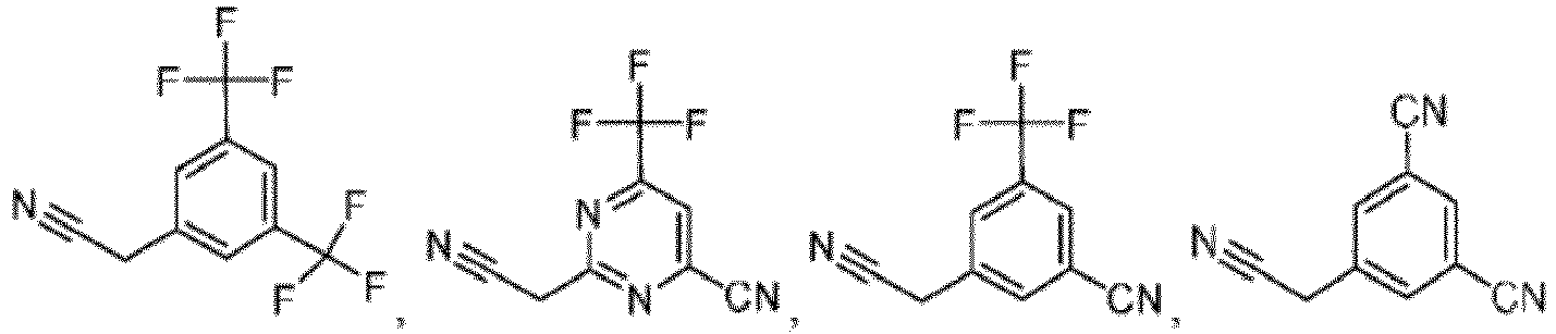

- Composé selon l'une quelconque des revendications 1 à 8, l'un parmi R1, R2, R4 et R5 étant choisi parmi CN, C1 à Ce alkyle partiellement fluoré ou perfluoré et les autres R1, R2, R4 et R5 étant indépendamment choisis parmi Cl ou F.
- Dispositif électronique organique comprenant une couche d'anode, une couche de cathode et au moins une couche de semi-conducteur organique, l'au moins une couche de semi-conducteur organique étant agencée entre la couche d'anode et la couche de cathode, et l'au moins une couche de semi-conducteur organique comprenant un composé de formule (I).
- Dispositif électronique organique selon la revendication 10, la couche de semi-conducteur organique comprenant une composition comprenant un composé de formule (IV) et au moins un composé de formule (IVa) à (IVd)


- Dispositif électronique organique selon la revendication 10 ou 11, le dispositif électronique organique comprenant au moins une couche photoactive et l'au moins une parmi l'au moins une couche de semi-conducteur organique étant agencée entre l'anode et l'au moins une couche photoactive.
- Dispositif électronique organique selon l'une quelconque des revendications 10 à 12, le dispositif électronique organique comprenant au moins deux couches photoactive, au moins l'une parmi l'au moins une couche de semi-conducteur organique étant agencée entre la première et la deuxième couche photoactive.
- Dispositif électronique organique selon l'une quelconque des revendications 10 à 13, le dispositif organique électronique étant un dispositif électroluminescent, préférablement une diode organique émettrice de lumière.
- Dispositif d'affichage comprenant un dispositif électronique organique selon l'une quelconque des revendications 10 à 14.
Applications Claiming Priority (10)
| Application Number | Priority Date | Filing Date | Title |
|---|---|---|---|
| EP20181398.7A EP3930023B1 (fr) | 2020-06-22 | 2020-06-22 | Dispositif électronique organique comprenant un composé de formule (1), dispositif d'affichage comprenant le dispositif électronique organique, ainsi que composés de formule (1) à utiliser dans des dispositifs électroniques organiques |
| EP20181408.4A EP3930024B1 (fr) | 2020-06-22 | 2020-06-22 | Dispositif électronique organique et dispositif d'affichage comprenant le dispositif électronique organique ainsi qu'une composition destinée à être utilisée dans des dispositifs électroniques organiques |
| EP20181386.2A EP3930022A1 (fr) | 2020-06-22 | 2020-06-22 | Dispositif électronique organique et dispositif d'affichage comprenant le dispositif électronique organique ainsi qu'une composition destinée à être utilisée dans des dispositifs électroniques organiques |
| EP20203458.3A EP3989304A1 (fr) | 2020-10-22 | 2020-10-22 | Composé organique de formule (i) pour une utilisation dans des dispositifs électroniques organiques, dispositif électronique organique comprenant un composé de formule (i) et dispositif d'affichage comprenant le dispositif électronique organique |
| EP20203463.3A EP3989305A1 (fr) | 2020-10-22 | 2020-10-22 | Dispositif électronique organique comprenant un composé de formule (1), dispositif d'affichage comprenant le dispositif électronique organique, ainsi que composés de formule (1) à utiliser dans des dispositifs électroniques organiques |
| EP20203457.5A EP3989303A1 (fr) | 2020-10-22 | 2020-10-22 | Composé organique de formule (i) à utiliser dans des dispositifs électroniques organiques, dispositif électronique organique comprenant un composé de formule (i) et dispositif d'affichage comprenant le dispositif électronique organique |
| EP20203447.6A EP3989302B1 (fr) | 2020-10-22 | 2020-10-22 | Composé organique de formule (i) pour une utilisation dans des dispositifs électroniques organiques, dispositif électronique organique comprenant un composé de formule (i) et dispositif d'affichage comprenant le dispositif électronique organique |
| EP20203460.9A EP3989301A1 (fr) | 2020-10-22 | 2020-10-22 | Dispositif électronique organique comprenant un composé de formule (1), dispositif d'affichage comprenant le dispositif électronique organique, ainsi que composés de formule (1) à utiliser dans des dispositifs électroniques organiques |
| PCT/EP2021/065949 WO2021250279A1 (fr) | 2020-06-12 | 2021-06-14 | Diode électroluminescente organique et dispositif la comprenant |
| PCT/EP2021/066603 WO2021259786A1 (fr) | 2020-06-22 | 2021-06-18 | Composé organique de formule (i) destiné à être utilisé dans des dispositifs électroniques organiques, dispositif électronique organique comprenant un composé de formule (i) et dispositif d'affichage comprenant le dispositif électronique organique |
Publications (2)
| Publication Number | Publication Date |
|---|---|
| EP4169085A1 EP4169085A1 (fr) | 2023-04-26 |
| EP4169085B1 true EP4169085B1 (fr) | 2024-04-03 |
Family
ID=79282020
Family Applications (12)
| Application Number | Title | Priority Date | Filing Date |
|---|---|---|---|
| EP21733809.4A Active EP4169090B1 (fr) | 2020-06-22 | 2021-06-18 | Dispositif électronique organique comprenant un composé de formule (i), dispositif d'affichage comprenant le dispositif électronique organique ainsi que composés de formule (i) destinés à être utilisés dans des dispositifs électroniques organiques |
| EP21733448.1A Active EP4168379B1 (fr) | 2020-06-22 | 2021-06-18 | Composé organique de formule (i) pour une utilisation dans des dispositifs électroniques organiques, dispositif électronique organique comprenant un composé de formule (i) et dispositif d'affichage comprenant le dispositif électronique organique |
| EP21733449.9A Pending EP4168380A2 (fr) | 2020-06-22 | 2021-06-18 | Dispositif électronique organique comprenant un composé de formule (i), dispositif d'affichage comprenant le dispositif électronique organique ainsi que composés de formule (i) destinés à être utilisés dans des dispositifs électroniques organiques |
| EP21733452.3A Active EP4169086B1 (fr) | 2020-06-22 | 2021-06-18 | Composé organique de formule (i) pour une utilisation dans des dispositifs électroniques organiques, dispositif électronique organique comprenant un composé de formule (i) et dispositif d'affichage comprenant le dispositif électronique organique |
| EP26160825.1A Pending EP4729512A2 (fr) | 2020-06-22 | 2021-06-18 | Composé organique de formule (i) pour utilisation dans des dispositifs électroniques organiques, dispositif électronique organique comprenant un composé de formule (i) |
| EP21733450.7A Active EP4169084B1 (fr) | 2020-06-22 | 2021-06-18 | Dispositif électronique organique comprenant un composé de formule (i), dispositif d'affichage comprenant le dispositif électronique organique |
| EP21733811.0A Active EP4169092B1 (fr) | 2020-06-22 | 2021-06-18 | Dispositif électronique organique et dispositif d'affichage comprenant le dispositif électronique organique ainsi qu'une composition destinée à être utilisée dans des dispositifs électroniques organiques |
| EP21733807.8A Active EP4169088B1 (fr) | 2020-06-22 | 2021-06-18 | Composé organique de formule (i) pour une utilisation dans des dispositifs électroniques organiques, dispositif électronique organique comprenant un composé de formule (i) et dispositif d'affichage comprenant le dispositif électronique organique |
| EP21733806.0A Active EP4169087B1 (fr) | 2020-06-22 | 2021-06-18 | Dispositif électronique organique et dispositif d'affichage comprenant le dispositif électronique organique ainsi qu'une composition destinée à être utilisée dans des dispositifs électroniques organiques |
| EP21733808.6A Pending EP4169089A1 (fr) | 2020-06-22 | 2021-06-18 | Composé organique de formule (i) destiné à être utilisé dans des dispositifs électroniques organiques, composition comprenant un composé de formule (iv) et au moins un composé de formule (iva) à (ivd), couche semi-conductrice organique comprenant le composé ou la composition, dispositif électronique organique comprenant la couche semi-conductrice organique, et dispositif d'affichage comprenant le dispositif électronique organique |
| EP21733810.2A Pending EP4169091A1 (fr) | 2020-06-22 | 2021-06-18 | Composé organique de formule (i) destiné à être utilisé dans des dispositifs électroniques organiques, composition comprenant un composé de formule (iv) et au moins un composé de formule (iva) à (ivd), couche semi-conductrice organique comprenant le composé ou la composition, dispositif électronique organique comprenant la couche semi-conductrice organique, et dispositif d'affichage comprenant le dispositif électronique organique |
| EP21733451.5A Active EP4169085B1 (fr) | 2020-06-22 | 2021-06-18 | Composé organique de formule (i) destiné à être utilisé dans des dispositifs électroniques organiques, dispositif électronique organique comprenant un composé de formule (i) et dispositif d'affichage comprenant le dispositif électronique organique |
Family Applications Before (11)
| Application Number | Title | Priority Date | Filing Date |
|---|---|---|---|
| EP21733809.4A Active EP4169090B1 (fr) | 2020-06-22 | 2021-06-18 | Dispositif électronique organique comprenant un composé de formule (i), dispositif d'affichage comprenant le dispositif électronique organique ainsi que composés de formule (i) destinés à être utilisés dans des dispositifs électroniques organiques |
| EP21733448.1A Active EP4168379B1 (fr) | 2020-06-22 | 2021-06-18 | Composé organique de formule (i) pour une utilisation dans des dispositifs électroniques organiques, dispositif électronique organique comprenant un composé de formule (i) et dispositif d'affichage comprenant le dispositif électronique organique |
| EP21733449.9A Pending EP4168380A2 (fr) | 2020-06-22 | 2021-06-18 | Dispositif électronique organique comprenant un composé de formule (i), dispositif d'affichage comprenant le dispositif électronique organique ainsi que composés de formule (i) destinés à être utilisés dans des dispositifs électroniques organiques |
| EP21733452.3A Active EP4169086B1 (fr) | 2020-06-22 | 2021-06-18 | Composé organique de formule (i) pour une utilisation dans des dispositifs électroniques organiques, dispositif électronique organique comprenant un composé de formule (i) et dispositif d'affichage comprenant le dispositif électronique organique |
| EP26160825.1A Pending EP4729512A2 (fr) | 2020-06-22 | 2021-06-18 | Composé organique de formule (i) pour utilisation dans des dispositifs électroniques organiques, dispositif électronique organique comprenant un composé de formule (i) |
| EP21733450.7A Active EP4169084B1 (fr) | 2020-06-22 | 2021-06-18 | Dispositif électronique organique comprenant un composé de formule (i), dispositif d'affichage comprenant le dispositif électronique organique |
| EP21733811.0A Active EP4169092B1 (fr) | 2020-06-22 | 2021-06-18 | Dispositif électronique organique et dispositif d'affichage comprenant le dispositif électronique organique ainsi qu'une composition destinée à être utilisée dans des dispositifs électroniques organiques |
| EP21733807.8A Active EP4169088B1 (fr) | 2020-06-22 | 2021-06-18 | Composé organique de formule (i) pour une utilisation dans des dispositifs électroniques organiques, dispositif électronique organique comprenant un composé de formule (i) et dispositif d'affichage comprenant le dispositif électronique organique |
| EP21733806.0A Active EP4169087B1 (fr) | 2020-06-22 | 2021-06-18 | Dispositif électronique organique et dispositif d'affichage comprenant le dispositif électronique organique ainsi qu'une composition destinée à être utilisée dans des dispositifs électroniques organiques |
| EP21733808.6A Pending EP4169089A1 (fr) | 2020-06-22 | 2021-06-18 | Composé organique de formule (i) destiné à être utilisé dans des dispositifs électroniques organiques, composition comprenant un composé de formule (iv) et au moins un composé de formule (iva) à (ivd), couche semi-conductrice organique comprenant le composé ou la composition, dispositif électronique organique comprenant la couche semi-conductrice organique, et dispositif d'affichage comprenant le dispositif électronique organique |
| EP21733810.2A Pending EP4169091A1 (fr) | 2020-06-22 | 2021-06-18 | Composé organique de formule (i) destiné à être utilisé dans des dispositifs électroniques organiques, composition comprenant un composé de formule (iv) et au moins un composé de formule (iva) à (ivd), couche semi-conductrice organique comprenant le composé ou la composition, dispositif électronique organique comprenant la couche semi-conductrice organique, et dispositif d'affichage comprenant le dispositif électronique organique |
Country Status (8)
| Country | Link |
|---|---|
| US (11) | US20230240137A1 (fr) |
| EP (12) | EP4169090B1 (fr) |
| JP (5) | JP7771107B2 (fr) |
| KR (11) | KR20230028427A (fr) |
| CN (10) | CN115918300A (fr) |
| HU (3) | HUE068204T2 (fr) |
| TW (11) | TWI891817B (fr) |
| WO (11) | WO2021259792A1 (fr) |
Families Citing this family (4)
| Publication number | Priority date | Publication date | Assignee | Title |
|---|---|---|---|---|
| WO2021259792A1 (fr) * | 2020-06-22 | 2021-12-30 | Novaled Gmbh | Composé organique de formule (i) destiné à être utilisé dans des dispositifs électroniques organiques, composition comprenant un composé de formule (iv) et au moins un composé de formule (iva) à (ivd), couche semi-conductrice organique comprenant le composé ou la composition, dispositif électronique organique comprenant la couche semi-conductrice organique, et dispositif d'affichage comprenant le dispositif électronique organique |
| EP3989303A1 (fr) * | 2020-10-22 | 2022-04-27 | Novaled GmbH | Composé organique de formule (i) à utiliser dans des dispositifs électroniques organiques, dispositif électronique organique comprenant un composé de formule (i) et dispositif d'affichage comprenant le dispositif électronique organique |
| EP3989304A1 (fr) * | 2020-10-22 | 2022-04-27 | Novaled GmbH | Composé organique de formule (i) pour une utilisation dans des dispositifs électroniques organiques, dispositif électronique organique comprenant un composé de formule (i) et dispositif d'affichage comprenant le dispositif électronique organique |
| EP4572587A1 (fr) * | 2023-12-12 | 2025-06-18 | Novaled GmbH | Dispositif électroluminescent organique et dispositif d'affichage |
Family Cites Families (69)
| Publication number | Priority date | Publication date | Assignee | Title |
|---|---|---|---|---|
| KR100260075B1 (ko) * | 1998-06-02 | 2000-07-01 | 손욱 | 플루오로화 아릴기를 함유한 완전 공액된 유기 전기 발광 고분자 조성물 및 그 제조방법 |
| US6872472B2 (en) * | 2002-02-15 | 2005-03-29 | Eastman Kodak Company | Providing an organic electroluminescent device having stacked electroluminescent units |
| JP3960131B2 (ja) * | 2002-06-05 | 2007-08-15 | コニカミノルタホールディングス株式会社 | 有機エレクトロルミネッセンス素子材料、及びそれを用いた有機エレクトロルミネッセンス素子および表示装置 |
| JP2005340121A (ja) * | 2004-05-31 | 2005-12-08 | Konica Minolta Holdings Inc | 有機エレクトロルミネッセンス素子、照明装置及び表示装置 |
| EP3076451B1 (fr) * | 2007-04-30 | 2019-03-06 | Novaled GmbH | Connexions de matiere d'oxydes de carbone, de matiere de pseudo oxyde de carbone et radiales tout comme leur utilisation |
| KR100951441B1 (ko) * | 2007-09-19 | 2010-04-07 | 덕산하이메탈(주) | 정공주입층/정공수송층 물질 및 이를 포함하는유기전계발광소자 |
| US8057712B2 (en) * | 2008-04-29 | 2011-11-15 | Novaled Ag | Radialene compounds and their use |
| EP2180029B1 (fr) | 2008-10-23 | 2011-07-27 | Novaled AG | Composés de Radialène et leur utilisation |
| US8603642B2 (en) * | 2009-05-13 | 2013-12-10 | Global Oled Technology Llc | Internal connector for organic electronic devices |
| KR101084177B1 (ko) | 2009-11-30 | 2011-11-17 | 삼성모바일디스플레이주식회사 | 유기 발광 디스플레이 장치 및 그의 제조 방법 |
| KR101766709B1 (ko) * | 2010-04-27 | 2017-08-09 | 노발레드 게엠베하 | 유기 반도전성 물질 및 전자 부품 |
| US20110315967A1 (en) * | 2010-06-24 | 2011-12-29 | Basf Se | Organic field effect transistor with improved current on/off ratio and controllable threshold shift |
| CN102074658B (zh) * | 2010-11-01 | 2014-08-27 | 中国科学院长春应用化学研究所 | 电荷产生层、叠层有机发光二极管及其制备方法 |
| US20130306961A1 (en) * | 2011-02-11 | 2013-11-21 | Idemitsu Kosen Co. Ltd | Organic light emitting device and materials for use in same |
| TWI526418B (zh) * | 2011-03-01 | 2016-03-21 | 諾瓦發光二極體股份公司 | 有機半導體材料及有機組成物 |
| KR101826730B1 (ko) * | 2012-02-14 | 2018-02-08 | 덕산네오룩스 주식회사 | 오원자 헤테로 고리를 포함하는 유기전기소자용 화합물, 이를 포함하는 유기전기소자 및 그 전자 장치 |
| EP2684932B8 (fr) * | 2012-07-09 | 2016-12-21 | Hodogaya Chemical Co., Ltd. | Matériau de matrice dopé avec une composé mesomeric radialène |
| CN103664748B (zh) * | 2012-09-03 | 2016-05-11 | 乐金显示有限公司 | 芘化合物以及包含该化合物的有机发光二极管设备 |
| EP2722908A1 (fr) | 2012-10-17 | 2014-04-23 | Novaled AG | Diode électroluminescente organique phosphorescente et matières de transport de trous pour diodes électroluminescentes phosphorescentes |
| KR102000208B1 (ko) * | 2012-12-20 | 2019-07-16 | 삼성디스플레이 주식회사 | 유기 발광 소자 |
| EP2826768A1 (fr) * | 2013-07-15 | 2015-01-21 | Novaled GmbH | Procédé de fabrication de 1,2,3-triylidénétris(cyanométhanylylidène)tris(2,3,5,6-tétrafluorobenzonitrile)-cyclopropane |
| KR102287012B1 (ko) * | 2014-05-28 | 2021-08-09 | 덕산네오룩스 주식회사 | 유기전기 소자용 화합물, 이를 이용한 유기전기소자 및 그 전자 장치 |
| GB2527606A (en) * | 2014-06-27 | 2015-12-30 | Cambridge Display Tech Ltd | Charge-transfer salt |
| EP2963696A1 (fr) * | 2014-07-04 | 2016-01-06 | Novaled GmbH | Diode électroluminescente organique (OLED) comprenant un empilement de couches de transport d'électrons comprenant différents composés de lithium |
| EP3034489A1 (fr) | 2014-12-16 | 2016-06-22 | Novaled GmbH | 1,2,3-triylidenetris (cyanomethanylylidene) cyclopropanes substitués pour VTE, dispositifs électroniques et matériaux semi-conducteurs les utilisant |
| EP3171418B1 (fr) * | 2015-11-23 | 2024-12-11 | Novaled GmbH | Couche semi-conductrice organique comprenant des composés d'oxyde de phosphine |
| KR102615636B1 (ko) * | 2016-01-13 | 2023-12-20 | 삼성디스플레이 주식회사 | 유기 발광 소자 |
| KR20170093274A (ko) * | 2016-02-03 | 2017-08-16 | 주식회사 동진쎄미켐 | 유기발광소자 |
| EP3208863B1 (fr) * | 2016-02-22 | 2019-10-23 | Novaled GmbH | Matériau semi-conducteur de transport de charge et dispositif électronique le comprenant |
| EP3252837B1 (fr) * | 2016-05-30 | 2021-05-05 | Novaled GmbH | Diode électroluminescente organique comprenant une couche semi-conductrice organique |
| EP3252841B1 (fr) * | 2016-05-30 | 2026-04-01 | Novaled GmbH | Diode électroluminescente organique comprenant une couche semi-conductrice organique |
| CN107799656B (zh) * | 2016-09-07 | 2019-12-06 | 元太科技工业股份有限公司 | 有机发光元件 |
| EP3312171B1 (fr) * | 2016-10-24 | 2019-07-31 | Novaled GmbH | Composé pour dispositif électronique et dispositif d'affichage et dispositif électronique |
| EP3336918B1 (fr) * | 2016-12-13 | 2020-09-02 | Novaled GmbH | Procédé d'éclairage par lumière flash et éléments de dispositif électronique organique ainsi obtenus |
| EP3583636B1 (fr) * | 2017-02-20 | 2023-05-24 | Novaled GmbH | Dispositif elelctronique procede de fabrication et compose |
| EP3605638B1 (fr) * | 2017-03-28 | 2023-11-08 | Hodogaya Chemical Co., Ltd. | Dispositif électroluminescent organique |
| EP3382770B1 (fr) * | 2017-03-30 | 2023-09-20 | Novaled GmbH | Composition d'encre pour former une couche organique d'un semi-conducteur |
| CN106848084B (zh) * | 2017-03-31 | 2019-12-17 | 上海天马有机发光显示技术有限公司 | 一种oled显示面板、制作方法及含有其的电子设备 |
| EP3407401A1 (fr) * | 2017-05-23 | 2018-11-28 | Novaled GmbH | Dispositif électronique organique comprenant une couche semi-conductrice organique et un dispositif |
| GB2563430A (en) * | 2017-06-15 | 2018-12-19 | Sumitomo Chemical Co | Compound |
| US11767299B2 (en) * | 2017-06-23 | 2023-09-26 | Merck Patent Gmbh | Materials for organic electroluminescent devices |
| CN109216565B (zh) * | 2017-06-30 | 2021-05-18 | 昆山国显光电有限公司 | 有机电致发光器件及其制备方法 |
| CN109326741A (zh) * | 2017-08-01 | 2019-02-12 | 江苏三月光电科技有限公司 | 一种含有氮杂苯类化合物的有机发光器件 |
| EP3503240B1 (fr) * | 2017-12-21 | 2024-11-20 | Novaled GmbH | Couche à semi-conducteur organique |
| CN108365127A (zh) * | 2018-02-13 | 2018-08-03 | 长春海谱润斯科技有限公司 | 一种有机半导电性材料及其有机发光器件 |
| EP3527557A1 (fr) * | 2018-02-16 | 2019-08-21 | Novaled GmbH | Composés n-hétéroarylène |
| CN111201623B (zh) * | 2018-02-28 | 2023-11-10 | 株式会社Lg化学 | 有机发光二极管 |
| EP3556753B1 (fr) * | 2018-04-18 | 2023-10-11 | Novaled GmbH | Composé et couche semiconductrice organique, dispositif électronique organique, dispositif d'affichage et dispositif d'éclairage le comprenant |
| CN108774515A (zh) * | 2018-06-04 | 2018-11-09 | 长春海谱润斯科技有限公司 | 一种有机发光组合材料及其有机发光器件 |
| CN108735911B (zh) | 2018-06-04 | 2020-04-14 | 长春海谱润斯科技有限公司 | 一种有机发光器件 |
| EP3591725A1 (fr) * | 2018-07-02 | 2020-01-08 | Novaled GmbH | Dispositif électronique, son procédé de préparation et dispositif d'affichage le comprenant |
| DE102018118278B4 (de) * | 2018-07-27 | 2025-02-20 | Novaled Gmbh | Elektronische Vorrichtung, Anzeigevorrichtung, Verfahren zum Herstellen derselben und eine Verbindung |
| CN109081791A (zh) * | 2018-08-03 | 2018-12-25 | 瑞声科技(南京)有限公司 | 一种有机半导体材料及发光器件 |
| DE102018122708B4 (de) * | 2018-09-17 | 2025-02-20 | Novaled Gmbh | Organische elektronische Vorrichtung, organisches halbleitendes Material und eine Boranverbindung |
| EP3643720B1 (fr) * | 2018-10-23 | 2021-09-29 | Novaled GmbH | Composés organiques, couche semi-conductrice organique et dispositif électronique organique |
| CN109320437A (zh) * | 2018-11-13 | 2019-02-12 | 长春海谱润斯科技有限公司 | 有机电致发光器件用化合物及包含其的有机电致发光器件 |
| CN109320426A (zh) * | 2018-11-16 | 2019-02-12 | 长春海谱润斯科技有限公司 | 有机电致发光器件用材料及包含其的有机电致发光器件 |
| EP3667755A1 (fr) * | 2018-12-14 | 2020-06-17 | Novaled GmbH | Dispositif électroluminescent organique, son procédé de fabrication et composition pour utilisation en son sein |
| CN109560209A (zh) * | 2018-12-14 | 2019-04-02 | 长春海谱润斯科技有限公司 | 一种用于空穴注入层的混合物及其有机发光器件 |
| CN112624990A (zh) * | 2019-10-08 | 2021-04-09 | 广州华睿光电材料有限公司 | 含氮杂环取代的环丙烷类化合物及其应用 |
| CN112687811B (zh) * | 2019-10-17 | 2023-09-12 | 北京夏禾科技有限公司 | 一种有机电致发光器件 |
| TW202116785A (zh) * | 2019-10-28 | 2021-05-01 | 日商東麗股份有限公司 | 包含吡咯亞甲基硼錯合物的發光元件材料、發光元件、顯示裝置及照明裝置 |
| CN110938085B (zh) * | 2019-12-04 | 2021-06-08 | 宁波卢米蓝新材料有限公司 | 一种轴烯化合物及其制备方法和应用 |
| WO2021259792A1 (fr) * | 2020-06-22 | 2021-12-30 | Novaled Gmbh | Composé organique de formule (i) destiné à être utilisé dans des dispositifs électroniques organiques, composition comprenant un composé de formule (iv) et au moins un composé de formule (iva) à (ivd), couche semi-conductrice organique comprenant le composé ou la composition, dispositif électronique organique comprenant la couche semi-conductrice organique, et dispositif d'affichage comprenant le dispositif électronique organique |
| CN116783159A (zh) * | 2021-01-10 | 2023-09-19 | 浙江光昊光电科技有限公司 | 有机化合物及其在有机电子器件的应用 |
| CN118435727A (zh) * | 2021-12-20 | 2024-08-02 | 诺瓦尔德股份有限公司 | 包含式(i)的化合物的电荷产生层、包含电荷产生层的有机电子器件和显示装置以及式(i)的化合物 |
| EP4287282A1 (fr) * | 2022-06-03 | 2023-12-06 | Novaled GmbH | Dispositif électroluminescent organique comprenant un composé de formule (i) et un composé de formule (ii), et dispositif d'affichage comprenant le dispositif électroluminescent organique |
| EP4533925A1 (fr) * | 2022-06-03 | 2025-04-09 | Novaled GmbH | Dispositif électroluminescent organique comprenant un composé de formule (i) et un composé de formule (ii), et dispositif d'affichage comprenant le dispositif électroluminescent organique |
| EP4387416A1 (fr) * | 2022-12-15 | 2024-06-19 | Novaled GmbH | Dispositif électroluminescent organique et dispositif d'affichage comprenant le dispositif électroluminescent organique |
-
2021
- 2021-06-18 WO PCT/EP2021/066612 patent/WO2021259792A1/fr not_active Ceased
- 2021-06-18 KR KR1020237002139A patent/KR20230028427A/ko active Pending
- 2021-06-18 HU HUE21733451A patent/HUE068204T2/hu unknown
- 2021-06-18 CN CN202180044264.5A patent/CN115918300A/zh active Pending
- 2021-06-18 KR KR1020237002140A patent/KR20230028774A/ko active Pending
- 2021-06-18 TW TW110122298A patent/TWI891817B/zh active
- 2021-06-18 US US18/002,013 patent/US20230240137A1/en active Pending
- 2021-06-18 WO PCT/EP2021/066604 patent/WO2021259787A1/fr not_active Ceased
- 2021-06-18 EP EP21733809.4A patent/EP4169090B1/fr active Active
- 2021-06-18 JP JP2022579682A patent/JP7771107B2/ja active Active
- 2021-06-18 US US18/002,609 patent/US20230240139A1/en active Pending
- 2021-06-18 JP JP2022579040A patent/JP2023530520A/ja active Pending
- 2021-06-18 JP JP2022579680A patent/JP2023531688A/ja active Pending
- 2021-06-18 US US18/002,158 patent/US20230232712A1/en active Pending
- 2021-06-18 KR KR1020237002132A patent/KR20230028769A/ko active Pending
- 2021-06-18 KR KR1020237002123A patent/KR20230027216A/ko active Pending
- 2021-06-18 WO PCT/EP2021/066597 patent/WO2021259782A2/fr not_active Ceased
- 2021-06-18 EP EP21733448.1A patent/EP4168379B1/fr active Active
- 2021-06-18 HU HUE21733811A patent/HUE067638T2/hu unknown
- 2021-06-18 KR KR1020237002133A patent/KR20230028770A/ko active Pending
- 2021-06-18 TW TW110122344A patent/TWI865790B/zh active
- 2021-06-18 CN CN202180044230.6A patent/CN116076169A/zh active Pending
- 2021-06-18 WO PCT/EP2021/066610 patent/WO2021259791A1/fr not_active Ceased
- 2021-06-18 EP EP21733449.9A patent/EP4168380A2/fr active Pending
- 2021-06-18 EP EP21733452.3A patent/EP4169086B1/fr active Active
- 2021-06-18 WO PCT/EP2021/066613 patent/WO2021259793A1/fr not_active Ceased
- 2021-06-18 WO PCT/EP2021/066606 patent/WO2021259789A1/fr not_active Ceased
- 2021-06-18 US US18/002,604 patent/US20230240138A1/en active Pending
- 2021-06-18 EP EP26160825.1A patent/EP4729512A2/fr active Pending
- 2021-06-18 WO PCT/EP2021/066603 patent/WO2021259786A1/fr not_active Ceased
- 2021-06-18 TW TW110122435A patent/TWI874671B/zh active
- 2021-06-18 TW TW110122346A patent/TWI876063B/zh active
- 2021-06-18 KR KR1020237002135A patent/KR20230028772A/ko active Pending
- 2021-06-18 EP EP21733450.7A patent/EP4169084B1/fr active Active
- 2021-06-18 KR KR1020237002138A patent/KR102919031B1/ko active Active
- 2021-06-18 WO PCT/EP2021/066607 patent/WO2021259790A1/fr not_active Ceased
- 2021-06-18 TW TW110122345A patent/TWI865791B/zh active
- 2021-06-18 US US18/002,008 patent/US20230247901A1/en active Pending
- 2021-06-18 EP EP21733811.0A patent/EP4169092B1/fr active Active
- 2021-06-18 WO PCT/EP2021/066605 patent/WO2021259788A1/fr not_active Ceased
- 2021-06-18 TW TW110122434A patent/TWI881141B/zh active
- 2021-06-18 US US18/002,088 patent/US20230232711A1/en active Pending
- 2021-06-18 EP EP21733807.8A patent/EP4169088B1/fr active Active
- 2021-06-18 TW TW110122294A patent/TWI890813B/zh active
- 2021-06-18 TW TW110122340A patent/TWI906315B/zh active
- 2021-06-18 KR KR1020237002122A patent/KR20230028424A/ko active Pending
- 2021-06-18 US US18/002,003 patent/US20230247900A1/en active Pending
- 2021-06-18 CN CN202180045206.4A patent/CN115804267A/zh active Pending
- 2021-06-18 WO PCT/EP2021/066602 patent/WO2021259785A1/fr not_active Ceased
- 2021-06-18 CN CN202180044582.1A patent/CN115943759A/zh active Pending
- 2021-06-18 US US18/002,082 patent/US20230232710A1/en active Pending
- 2021-06-18 JP JP2022579037A patent/JP7842040B2/ja active Active
- 2021-06-18 US US18/002,562 patent/US20230240132A1/en active Pending
- 2021-06-18 CN CN202180044546.5A patent/CN115943758A/zh active Pending
- 2021-06-18 CN CN202180044197.7A patent/CN115918299A/zh active Pending
- 2021-06-18 EP EP21733806.0A patent/EP4169087B1/fr active Active
- 2021-06-18 WO PCT/EP2021/066601 patent/WO2021259784A2/fr not_active Ceased
- 2021-06-18 US US18/002,172 patent/US20230227401A1/en active Pending
- 2021-06-18 TW TW110122341A patent/TW202231625A/zh unknown
- 2021-06-18 EP EP21733808.6A patent/EP4169089A1/fr active Pending
- 2021-06-18 US US18/002,144 patent/US20230225141A1/en active Pending
- 2021-06-18 CN CN202180044232.5A patent/CN115885598A/zh active Pending
- 2021-06-18 KR KR1020237002134A patent/KR20230028771A/ko active Pending
- 2021-06-18 TW TW110122342A patent/TW202231624A/zh unknown
- 2021-06-18 EP EP21733810.2A patent/EP4169091A1/fr active Pending
- 2021-06-18 KR KR1020237002121A patent/KR20230028768A/ko not_active Ceased
- 2021-06-18 CN CN202180044505.6A patent/CN115867531A/zh active Pending
- 2021-06-18 TW TW110122281A patent/TWI870601B/zh active
- 2021-06-18 CN CN202180044543.1A patent/CN115943757A/zh active Pending
- 2021-06-18 HU HUE21733806A patent/HUE066882T2/hu unknown
- 2021-06-18 EP EP21733451.5A patent/EP4169085B1/fr active Active
- 2021-06-18 KR KR1020237002120A patent/KR102887494B1/ko active Active
- 2021-06-18 JP JP2022579039A patent/JP7844359B2/ja active Active
- 2021-06-18 CN CN202180044534.2A patent/CN116058109B/zh active Active
Also Published As
Similar Documents
| Publication | Publication Date | Title |
|---|---|---|
| EP4244911B1 (fr) | Dispositif électronique organique comprenant un composé de formule (1), dispositif d'affichage comprenant le dispositif électronique organique, ainsi que composés de formule (1) à utiliser dans des dispositifs électroniques organiques | |
| EP4169085B1 (fr) | Composé organique de formule (i) destiné à être utilisé dans des dispositifs électroniques organiques, dispositif électronique organique comprenant un composé de formule (i) et dispositif d'affichage comprenant le dispositif électronique organique | |
| EP3989305A1 (fr) | Dispositif électronique organique comprenant un composé de formule (1), dispositif d'affichage comprenant le dispositif électronique organique, ainsi que composés de formule (1) à utiliser dans des dispositifs électroniques organiques | |
| EP4284780B1 (fr) | Composé organique de formule (i) pour l'utilisation dans des dispositifs électroniques organiques, dispositif électronique organique comprenant ce composé et dispositif d'affichage comprenant le dispositif électronique organique | |
| EP3930024B1 (fr) | Dispositif électronique organique et dispositif d'affichage comprenant le dispositif électronique organique ainsi qu'une composition destinée à être utilisée dans des dispositifs électroniques organiques | |
| EP3989302B1 (fr) | Composé organique de formule (i) pour une utilisation dans des dispositifs électroniques organiques, dispositif électronique organique comprenant un composé de formule (i) et dispositif d'affichage comprenant le dispositif électronique organique | |
| EP3930023B1 (fr) | Dispositif électronique organique comprenant un composé de formule (1), dispositif d'affichage comprenant le dispositif électronique organique, ainsi que composés de formule (1) à utiliser dans des dispositifs électroniques organiques | |
| EP4106034B1 (fr) | Dispositif électronique organique comprenant un composé métallique comportant des cations métalliques et au moins un anion de borate de formule (i), dispositif d'affichage comprenant le dispositif électronique organique, utilisation du composé métallique dans un dispositif électronique organique et procédé de préparation du dispositif électronique organique | |
| EP3989304A1 (fr) | Composé organique de formule (i) pour une utilisation dans des dispositifs électroniques organiques, dispositif électronique organique comprenant un composé de formule (i) et dispositif d'affichage comprenant le dispositif électronique organique | |
| EP4155303A1 (fr) | Composé organique de formule (i) pour une utilisation dans des dispositifs électroniques organiques, composition comprenant un composé de formule (iv) et au moins un composé de formule (iva) à (ivd), couche semi-conductrice organique comprenant le composé ou la composition, dispositif électronique organique comprenant la couche semi-conductrice organique et dispositif d'affichage comprenant le dispositif électronique organique | |
| EP3989303A1 (fr) | Composé organique de formule (i) à utiliser dans des dispositifs électroniques organiques, dispositif électronique organique comprenant un composé de formule (i) et dispositif d'affichage comprenant le dispositif électronique organique | |
| EP3989301A1 (fr) | Dispositif électronique organique comprenant un composé de formule (1), dispositif d'affichage comprenant le dispositif électronique organique, ainsi que composés de formule (1) à utiliser dans des dispositifs électroniques organiques |
Legal Events
| Date | Code | Title | Description |
|---|---|---|---|
| STAA | Information on the status of an ep patent application or granted ep patent |
Free format text: STATUS: UNKNOWN |
|
| STAA | Information on the status of an ep patent application or granted ep patent |
Free format text: STATUS: THE INTERNATIONAL PUBLICATION HAS BEEN MADE |
|
| PUAI | Public reference made under article 153(3) epc to a published international application that has entered the european phase |
Free format text: ORIGINAL CODE: 0009012 |
|
| STAA | Information on the status of an ep patent application or granted ep patent |
Free format text: STATUS: REQUEST FOR EXAMINATION WAS MADE |
|
| 17P | Request for examination filed |
Effective date: 20230118 |
|
| AK | Designated contracting states |
Kind code of ref document: A1 Designated state(s): AL AT BE BG CH CY CZ DE DK EE ES FI FR GB GR HR HU IE IS IT LI LT LU LV MC MK MT NL NO PL PT RO RS SE SI SK SM TR |
|
| DAV | Request for validation of the european patent (deleted) | ||
| DAX | Request for extension of the european patent (deleted) | ||
| REG | Reference to a national code |
Ref country code: DE Ref legal event code: R079 Ref document number: 602021011368 Country of ref document: DE Free format text: PREVIOUS MAIN CLASS: H01L0051540000 Ipc: H10K0085600000 Ref country code: DE Ref legal event code: R079 Free format text: PREVIOUS MAIN CLASS: H01L0051540000 Ipc: H10K0085600000 |
|
| GRAP | Despatch of communication of intention to grant a patent |
Free format text: ORIGINAL CODE: EPIDOSNIGR1 |
|
| STAA | Information on the status of an ep patent application or granted ep patent |
Free format text: STATUS: GRANT OF PATENT IS INTENDED |
|
| RIC1 | Information provided on ipc code assigned before grant |
Ipc: H10K 50/17 20230101ALN20231214BHEP Ipc: C07D 251/24 20060101ALI20231214BHEP Ipc: C07D 239/26 20060101ALI20231214BHEP Ipc: C07D 213/84 20060101ALI20231214BHEP Ipc: C07D 213/61 20060101ALI20231214BHEP Ipc: C07C 255/51 20060101ALI20231214BHEP Ipc: C07C 255/37 20060101ALI20231214BHEP Ipc: C07C 255/35 20060101ALI20231214BHEP Ipc: H10K 85/60 20230101AFI20231214BHEP |
|
| INTG | Intention to grant announced |
Effective date: 20240104 |
|
| GRAS | Grant fee paid |
Free format text: ORIGINAL CODE: EPIDOSNIGR3 |
|
| GRAA | (expected) grant |
Free format text: ORIGINAL CODE: 0009210 |
|
| STAA | Information on the status of an ep patent application or granted ep patent |
Free format text: STATUS: THE PATENT HAS BEEN GRANTED |
|
| AK | Designated contracting states |
Kind code of ref document: B1 Designated state(s): AL AT BE BG CH CY CZ DE DK EE ES FI FR GB GR HR HU IE IS IT LI LT LU LV MC MK MT NL NO PL PT RO RS SE SI SK SM TR |
|
| REG | Reference to a national code |
Ref country code: CH Ref legal event code: EP |
|
| REG | Reference to a national code |
Ref country code: IE Ref legal event code: FG4D |
|
| REG | Reference to a national code |
Ref country code: DE Ref legal event code: R096 Ref document number: 602021011368 Country of ref document: DE |
|
| P01 | Opt-out of the competence of the unified patent court (upc) registered |
Effective date: 20240410 |
|
| REG | Reference to a national code |
Ref country code: LT Ref legal event code: MG9D |
|
| REG | Reference to a national code |
Ref country code: NL Ref legal event code: MP Effective date: 20240403 |
|
| REG | Reference to a national code |
Ref country code: AT Ref legal event code: MK05 Ref document number: 1673843 Country of ref document: AT Kind code of ref document: T Effective date: 20240403 |
|
| PG25 | Lapsed in a contracting state [announced via postgrant information from national office to epo] |
Ref country code: NL Free format text: LAPSE BECAUSE OF FAILURE TO SUBMIT A TRANSLATION OF THE DESCRIPTION OR TO PAY THE FEE WITHIN THE PRESCRIBED TIME-LIMIT Effective date: 20240403 |
|
| PG25 | Lapsed in a contracting state [announced via postgrant information from national office to epo] |
Ref country code: NL Free format text: LAPSE BECAUSE OF FAILURE TO SUBMIT A TRANSLATION OF THE DESCRIPTION OR TO PAY THE FEE WITHIN THE PRESCRIBED TIME-LIMIT Effective date: 20240403 |
|
| PG25 | Lapsed in a contracting state [announced via postgrant information from national office to epo] |
Ref country code: IS Free format text: LAPSE BECAUSE OF FAILURE TO SUBMIT A TRANSLATION OF THE DESCRIPTION OR TO PAY THE FEE WITHIN THE PRESCRIBED TIME-LIMIT Effective date: 20240803 |
|
| PG25 | Lapsed in a contracting state [announced via postgrant information from national office to epo] |
Ref country code: BG Free format text: LAPSE BECAUSE OF FAILURE TO SUBMIT A TRANSLATION OF THE DESCRIPTION OR TO PAY THE FEE WITHIN THE PRESCRIBED TIME-LIMIT Effective date: 20240403 |
|
| PG25 | Lapsed in a contracting state [announced via postgrant information from national office to epo] |
Ref country code: HR Free format text: LAPSE BECAUSE OF FAILURE TO SUBMIT A TRANSLATION OF THE DESCRIPTION OR TO PAY THE FEE WITHIN THE PRESCRIBED TIME-LIMIT Effective date: 20240403 Ref country code: FI Free format text: LAPSE BECAUSE OF FAILURE TO SUBMIT A TRANSLATION OF THE DESCRIPTION OR TO PAY THE FEE WITHIN THE PRESCRIBED TIME-LIMIT Effective date: 20240403 |
|
| PG25 | Lapsed in a contracting state [announced via postgrant information from national office to epo] |
Ref country code: GR Free format text: LAPSE BECAUSE OF FAILURE TO SUBMIT A TRANSLATION OF THE DESCRIPTION OR TO PAY THE FEE WITHIN THE PRESCRIBED TIME-LIMIT Effective date: 20240704 |
|
| PG25 | Lapsed in a contracting state [announced via postgrant information from national office to epo] |
Ref country code: PT Free format text: LAPSE BECAUSE OF FAILURE TO SUBMIT A TRANSLATION OF THE DESCRIPTION OR TO PAY THE FEE WITHIN THE PRESCRIBED TIME-LIMIT Effective date: 20240805 |
|
| PG25 | Lapsed in a contracting state [announced via postgrant information from national office to epo] |
Ref country code: ES Free format text: LAPSE BECAUSE OF FAILURE TO SUBMIT A TRANSLATION OF THE DESCRIPTION OR TO PAY THE FEE WITHIN THE PRESCRIBED TIME-LIMIT Effective date: 20240403 |
|
| PG25 | Lapsed in a contracting state [announced via postgrant information from national office to epo] |
Ref country code: CZ Free format text: LAPSE BECAUSE OF FAILURE TO SUBMIT A TRANSLATION OF THE DESCRIPTION OR TO PAY THE FEE WITHIN THE PRESCRIBED TIME-LIMIT Effective date: 20240403 |
|
| PG25 | Lapsed in a contracting state [announced via postgrant information from national office to epo] |
Ref country code: AT Free format text: LAPSE BECAUSE OF FAILURE TO SUBMIT A TRANSLATION OF THE DESCRIPTION OR TO PAY THE FEE WITHIN THE PRESCRIBED TIME-LIMIT Effective date: 20240403 |
|
| PG25 | Lapsed in a contracting state [announced via postgrant information from national office to epo] |
Ref country code: PL Free format text: LAPSE BECAUSE OF FAILURE TO SUBMIT A TRANSLATION OF THE DESCRIPTION OR TO PAY THE FEE WITHIN THE PRESCRIBED TIME-LIMIT Effective date: 20240403 |
|
| PG25 | Lapsed in a contracting state [announced via postgrant information from national office to epo] |
Ref country code: LV Free format text: LAPSE BECAUSE OF FAILURE TO SUBMIT A TRANSLATION OF THE DESCRIPTION OR TO PAY THE FEE WITHIN THE PRESCRIBED TIME-LIMIT Effective date: 20240403 |
|
| PG25 | Lapsed in a contracting state [announced via postgrant information from national office to epo] |
Ref country code: PT Free format text: LAPSE BECAUSE OF FAILURE TO SUBMIT A TRANSLATION OF THE DESCRIPTION OR TO PAY THE FEE WITHIN THE PRESCRIBED TIME-LIMIT Effective date: 20240805 Ref country code: PL Free format text: LAPSE BECAUSE OF FAILURE TO SUBMIT A TRANSLATION OF THE DESCRIPTION OR TO PAY THE FEE WITHIN THE PRESCRIBED TIME-LIMIT Effective date: 20240403 Ref country code: NO Free format text: LAPSE BECAUSE OF FAILURE TO SUBMIT A TRANSLATION OF THE DESCRIPTION OR TO PAY THE FEE WITHIN THE PRESCRIBED TIME-LIMIT Effective date: 20240703 Ref country code: LV Free format text: LAPSE BECAUSE OF FAILURE TO SUBMIT A TRANSLATION OF THE DESCRIPTION OR TO PAY THE FEE WITHIN THE PRESCRIBED TIME-LIMIT Effective date: 20240403 Ref country code: IS Free format text: LAPSE BECAUSE OF FAILURE TO SUBMIT A TRANSLATION OF THE DESCRIPTION OR TO PAY THE FEE WITHIN THE PRESCRIBED TIME-LIMIT Effective date: 20240803 Ref country code: HR Free format text: LAPSE BECAUSE OF FAILURE TO SUBMIT A TRANSLATION OF THE DESCRIPTION OR TO PAY THE FEE WITHIN THE PRESCRIBED TIME-LIMIT Effective date: 20240403 Ref country code: GR Free format text: LAPSE BECAUSE OF FAILURE TO SUBMIT A TRANSLATION OF THE DESCRIPTION OR TO PAY THE FEE WITHIN THE PRESCRIBED TIME-LIMIT Effective date: 20240704 Ref country code: FI Free format text: LAPSE BECAUSE OF FAILURE TO SUBMIT A TRANSLATION OF THE DESCRIPTION OR TO PAY THE FEE WITHIN THE PRESCRIBED TIME-LIMIT Effective date: 20240403 Ref country code: ES Free format text: LAPSE BECAUSE OF FAILURE TO SUBMIT A TRANSLATION OF THE DESCRIPTION OR TO PAY THE FEE WITHIN THE PRESCRIBED TIME-LIMIT Effective date: 20240403 Ref country code: CZ Free format text: LAPSE BECAUSE OF FAILURE TO SUBMIT A TRANSLATION OF THE DESCRIPTION OR TO PAY THE FEE WITHIN THE PRESCRIBED TIME-LIMIT Effective date: 20240403 Ref country code: BG Free format text: LAPSE BECAUSE OF FAILURE TO SUBMIT A TRANSLATION OF THE DESCRIPTION OR TO PAY THE FEE WITHIN THE PRESCRIBED TIME-LIMIT Effective date: 20240403 Ref country code: AT Free format text: LAPSE BECAUSE OF FAILURE TO SUBMIT A TRANSLATION OF THE DESCRIPTION OR TO PAY THE FEE WITHIN THE PRESCRIBED TIME-LIMIT Effective date: 20240403 Ref country code: RS Free format text: LAPSE BECAUSE OF FAILURE TO SUBMIT A TRANSLATION OF THE DESCRIPTION OR TO PAY THE FEE WITHIN THE PRESCRIBED TIME-LIMIT Effective date: 20240703 |
|
| REG | Reference to a national code |
Ref country code: HU Ref legal event code: AG4A Ref document number: E068204 Country of ref document: HU |
|
| REG | Reference to a national code |
Ref country code: DE Ref legal event code: R097 Ref document number: 602021011368 Country of ref document: DE |
|
| PG25 | Lapsed in a contracting state [announced via postgrant information from national office to epo] |
Ref country code: DK Free format text: LAPSE BECAUSE OF FAILURE TO SUBMIT A TRANSLATION OF THE DESCRIPTION OR TO PAY THE FEE WITHIN THE PRESCRIBED TIME-LIMIT Effective date: 20240403 |
|
| PG25 | Lapsed in a contracting state [announced via postgrant information from national office to epo] |
Ref country code: EE Free format text: LAPSE BECAUSE OF FAILURE TO SUBMIT A TRANSLATION OF THE DESCRIPTION OR TO PAY THE FEE WITHIN THE PRESCRIBED TIME-LIMIT Effective date: 20240403 |
|
| PG25 | Lapsed in a contracting state [announced via postgrant information from national office to epo] |
Ref country code: SK Free format text: LAPSE BECAUSE OF FAILURE TO SUBMIT A TRANSLATION OF THE DESCRIPTION OR TO PAY THE FEE WITHIN THE PRESCRIBED TIME-LIMIT Effective date: 20240403 Ref country code: RO Free format text: LAPSE BECAUSE OF FAILURE TO SUBMIT A TRANSLATION OF THE DESCRIPTION OR TO PAY THE FEE WITHIN THE PRESCRIBED TIME-LIMIT Effective date: 20240403 |
|
| PG25 | Lapsed in a contracting state [announced via postgrant information from national office to epo] |
Ref country code: SM Free format text: LAPSE BECAUSE OF FAILURE TO SUBMIT A TRANSLATION OF THE DESCRIPTION OR TO PAY THE FEE WITHIN THE PRESCRIBED TIME-LIMIT Effective date: 20240403 |
|
| PG25 | Lapsed in a contracting state [announced via postgrant information from national office to epo] |
Ref country code: SM Free format text: LAPSE BECAUSE OF FAILURE TO SUBMIT A TRANSLATION OF THE DESCRIPTION OR TO PAY THE FEE WITHIN THE PRESCRIBED TIME-LIMIT Effective date: 20240403 Ref country code: SK Free format text: LAPSE BECAUSE OF FAILURE TO SUBMIT A TRANSLATION OF THE DESCRIPTION OR TO PAY THE FEE WITHIN THE PRESCRIBED TIME-LIMIT Effective date: 20240403 Ref country code: RO Free format text: LAPSE BECAUSE OF FAILURE TO SUBMIT A TRANSLATION OF THE DESCRIPTION OR TO PAY THE FEE WITHIN THE PRESCRIBED TIME-LIMIT Effective date: 20240403 Ref country code: EE Free format text: LAPSE BECAUSE OF FAILURE TO SUBMIT A TRANSLATION OF THE DESCRIPTION OR TO PAY THE FEE WITHIN THE PRESCRIBED TIME-LIMIT Effective date: 20240403 Ref country code: DK Free format text: LAPSE BECAUSE OF FAILURE TO SUBMIT A TRANSLATION OF THE DESCRIPTION OR TO PAY THE FEE WITHIN THE PRESCRIBED TIME-LIMIT Effective date: 20240403 Ref country code: MC Free format text: LAPSE BECAUSE OF FAILURE TO SUBMIT A TRANSLATION OF THE DESCRIPTION OR TO PAY THE FEE WITHIN THE PRESCRIBED TIME-LIMIT Effective date: 20240403 |
|
| REG | Reference to a national code |
Ref country code: CH Ref legal event code: PL |
|
| PLBE | No opposition filed within time limit |
Free format text: ORIGINAL CODE: 0009261 |
|
| STAA | Information on the status of an ep patent application or granted ep patent |
Free format text: STATUS: NO OPPOSITION FILED WITHIN TIME LIMIT |
|
| PG25 | Lapsed in a contracting state [announced via postgrant information from national office to epo] |
Ref country code: LU Free format text: LAPSE BECAUSE OF NON-PAYMENT OF DUE FEES Effective date: 20240618 |
|
| 26N | No opposition filed |
Effective date: 20250106 |
|
| PG25 | Lapsed in a contracting state [announced via postgrant information from national office to epo] |
Ref country code: IE Free format text: LAPSE BECAUSE OF NON-PAYMENT OF DUE FEES Effective date: 20240618 |
|
| PG25 | Lapsed in a contracting state [announced via postgrant information from national office to epo] |
Ref country code: SI Free format text: LAPSE BECAUSE OF FAILURE TO SUBMIT A TRANSLATION OF THE DESCRIPTION OR TO PAY THE FEE WITHIN THE PRESCRIBED TIME-LIMIT Effective date: 20240403 Ref country code: BE Free format text: LAPSE BECAUSE OF NON-PAYMENT OF DUE FEES Effective date: 20240630 Ref country code: CH Free format text: LAPSE BECAUSE OF NON-PAYMENT OF DUE FEES Effective date: 20240630 |
|
| REG | Reference to a national code |
Ref country code: BE Ref legal event code: MM Effective date: 20240630 |
|
| PGFP | Annual fee paid to national office [announced via postgrant information from national office to epo] |
Ref country code: DE Payment date: 20250402 Year of fee payment: 5 |
|
| PGFP | Annual fee paid to national office [announced via postgrant information from national office to epo] |
Ref country code: GB Payment date: 20250401 Year of fee payment: 5 |
|
| PGFP | Annual fee paid to national office [announced via postgrant information from national office to epo] |
Ref country code: HU Payment date: 20250513 Year of fee payment: 5 Ref country code: FR Payment date: 20250409 Year of fee payment: 5 |
|
| PG25 | Lapsed in a contracting state [announced via postgrant information from national office to epo] |
Ref country code: SE Free format text: LAPSE BECAUSE OF FAILURE TO SUBMIT A TRANSLATION OF THE DESCRIPTION OR TO PAY THE FEE WITHIN THE PRESCRIBED TIME-LIMIT Effective date: 20240403 |
|
| PG25 | Lapsed in a contracting state [announced via postgrant information from national office to epo] |
Ref country code: CY Free format text: LAPSE BECAUSE OF FAILURE TO SUBMIT A TRANSLATION OF THE DESCRIPTION OR TO PAY THE FEE WITHIN THE PRESCRIBED TIME-LIMIT; INVALID AB INITIO Effective date: 20210618 |
|
| PG25 | Lapsed in a contracting state [announced via postgrant information from national office to epo] |
Ref country code: IT Free format text: LAPSE BECAUSE OF FAILURE TO SUBMIT A TRANSLATION OF THE DESCRIPTION OR TO PAY THE FEE WITHIN THE PRESCRIBED TIME-LIMIT Effective date: 20240403 |