EP4169723A2 - Verbrauchschip und antwortverfahren für verbrauchschip, verbrauchskartusche und speichermedium - Google Patents
Verbrauchschip und antwortverfahren für verbrauchschip, verbrauchskartusche und speichermedium Download PDFInfo
- Publication number
- EP4169723A2 EP4169723A2 EP21832471.3A EP21832471A EP4169723A2 EP 4169723 A2 EP4169723 A2 EP 4169723A2 EP 21832471 A EP21832471 A EP 21832471A EP 4169723 A2 EP4169723 A2 EP 4169723A2
- Authority
- EP
- European Patent Office
- Prior art keywords
- data
- consumable chip
- target data
- indicator
- printing device
- Prior art date
- Legal status (The legal status is an assumption and is not a legal conclusion. Google has not performed a legal analysis and makes no representation as to the accuracy of the status listed.)
- Granted
Links
Images



Classifications
-
- G—PHYSICS
- G06—COMPUTING OR CALCULATING; COUNTING
- G06F—ELECTRIC DIGITAL DATA PROCESSING
- G06F3/00—Input arrangements for transferring data to be processed into a form capable of being handled by the computer; Output arrangements for transferring data from processing unit to output unit, e.g. interface arrangements
- G06F3/12—Digital output to print unit, e.g. line printer, chain printer
- G06F3/1201—Dedicated interfaces to print systems
- G06F3/1223—Dedicated interfaces to print systems specifically adapted to use a particular technique
- G06F3/1237—Print job management
- G06F3/1238—Secure printing, e.g. user identification, user rights for device usage, unallowed content, blanking portions or fields of a page, releasing held jobs
-
- B—PERFORMING OPERATIONS; TRANSPORTING
- B41—PRINTING; LINING MACHINES; TYPEWRITERS; STAMPS
- B41J—TYPEWRITERS; SELECTIVE PRINTING MECHANISMS, i.e. MECHANISMS PRINTING OTHERWISE THAN FROM A FORME; CORRECTION OF TYPOGRAPHICAL ERRORS
- B41J2/00—Typewriters or selective printing mechanisms characterised by the printing or marking process for which they are designed
- B41J2/005—Typewriters or selective printing mechanisms characterised by the printing or marking process for which they are designed characterised by bringing liquid or particles selectively into contact with a printing material
- B41J2/01—Ink jet
- B41J2/17—Ink jet characterised by ink handling
- B41J2/175—Ink supply systems ; Circuit parts therefor
- B41J2/17503—Ink cartridges
- B41J2/17543—Cartridge presence detection or type identification
- B41J2/17546—Cartridge presence detection or type identification electronically
-
- B—PERFORMING OPERATIONS; TRANSPORTING
- B41—PRINTING; LINING MACHINES; TYPEWRITERS; STAMPS
- B41J—TYPEWRITERS; SELECTIVE PRINTING MECHANISMS, i.e. MECHANISMS PRINTING OTHERWISE THAN FROM A FORME; CORRECTION OF TYPOGRAPHICAL ERRORS
- B41J2/00—Typewriters or selective printing mechanisms characterised by the printing or marking process for which they are designed
- B41J2/005—Typewriters or selective printing mechanisms characterised by the printing or marking process for which they are designed characterised by bringing liquid or particles selectively into contact with a printing material
- B41J2/01—Ink jet
- B41J2/17—Ink jet characterised by ink handling
- B41J2/175—Ink supply systems ; Circuit parts therefor
- B41J2/17566—Ink level or ink residue control
-
- G—PHYSICS
- G03—PHOTOGRAPHY; CINEMATOGRAPHY; ANALOGOUS TECHNIQUES USING WAVES OTHER THAN OPTICAL WAVES; ELECTROGRAPHY; HOLOGRAPHY
- G03G—ELECTROGRAPHY; ELECTROPHOTOGRAPHY; MAGNETOGRAPHY
- G03G15/00—Apparatus for electrographic processes using a charge pattern
- G03G15/06—Apparatus for electrographic processes using a charge pattern for developing
- G03G15/08—Apparatus for electrographic processes using a charge pattern for developing using a solid developer, e.g. powder developer
- G03G15/0822—Arrangements for preparing, mixing, supplying or dispensing developer
- G03G15/0863—Arrangements for preparing, mixing, supplying or dispensing developer provided with identifying means or means for storing process- or use parameters, e.g. an electronic memory
-
- G—PHYSICS
- G06—COMPUTING OR CALCULATING; COUNTING
- G06F—ELECTRIC DIGITAL DATA PROCESSING
- G06F3/00—Input arrangements for transferring data to be processed into a form capable of being handled by the computer; Output arrangements for transferring data from processing unit to output unit, e.g. interface arrangements
- G06F3/12—Digital output to print unit, e.g. line printer, chain printer
- G06F3/1201—Dedicated interfaces to print systems
- G06F3/1202—Dedicated interfaces to print systems specifically adapted to achieve a particular effect
- G06F3/1222—Increasing security of the print job
-
- B—PERFORMING OPERATIONS; TRANSPORTING
- B41—PRINTING; LINING MACHINES; TYPEWRITERS; STAMPS
- B41J—TYPEWRITERS; SELECTIVE PRINTING MECHANISMS, i.e. MECHANISMS PRINTING OTHERWISE THAN FROM A FORME; CORRECTION OF TYPOGRAPHICAL ERRORS
- B41J2/00—Typewriters or selective printing mechanisms characterised by the printing or marking process for which they are designed
- B41J2/005—Typewriters or selective printing mechanisms characterised by the printing or marking process for which they are designed characterised by bringing liquid or particles selectively into contact with a printing material
- B41J2/01—Ink jet
- B41J2/17—Ink jet characterised by ink handling
- B41J2/175—Ink supply systems ; Circuit parts therefor
- B41J2/17566—Ink level or ink residue control
- B41J2002/17569—Ink level or ink residue control based on the amount printed or to be printed
-
- G—PHYSICS
- G03—PHOTOGRAPHY; CINEMATOGRAPHY; ANALOGOUS TECHNIQUES USING WAVES OTHER THAN OPTICAL WAVES; ELECTROGRAPHY; HOLOGRAPHY
- G03G—ELECTROGRAPHY; ELECTROPHOTOGRAPHY; MAGNETOGRAPHY
- G03G21/00—Arrangements not provided for by groups G03G13/00 - G03G19/00, e.g. cleaning, elimination of residual charge
- G03G21/16—Mechanical means for facilitating the maintenance of the apparatus, e.g. modular arrangements
- G03G21/18—Mechanical means for facilitating the maintenance of the apparatus, e.g. modular arrangements using a processing cartridge, whereby the process cartridge comprises at least two image processing means in a single unit
- G03G21/1875—Mechanical means for facilitating the maintenance of the apparatus, e.g. modular arrangements using a processing cartridge, whereby the process cartridge comprises at least two image processing means in a single unit provided with identifying means or means for storing process- or use parameters, e.g. lifetime of the cartridge
- G03G21/1878—Electronically readable memory
- G03G21/1889—Electronically readable memory for auto-setting of process parameters, lifetime, usage
Definitions
- Embodiments of this application relate to the field of office consumables, and in particular, to a consumable chip, a responding method for a consumable chip, a consumable cartridge, and a storage medium.
- a printing device is an indispensable device in modern life.
- a consumable cartridge such as an ink cartridge and a toner cartridge is required.
- a removable consumable chip such as a toner cartridge chip, is installed on the ink cartridge or the toner cartridge.
- the toner cartridge chip is configured to store data related to the toner cartridge, such as a toner color, a remaining toner quantity, a page output (a maximum value of a quantity of pages that can be printed), a quantity of printed pages, a manufacturer, and a production date.
- the printing device When the consumable chip communicates with the printing device, the printing device needs to verify whether the consumable chip is authentic and trustworthy. Therefore, a digital signature is generally stored in the consumable chip. When the digital signature is verified, it can indicate that the consumable chip is authentic and trustworthy. In some cases, when the consumable chip does not store a digital signature, the printing device also needs to communicate with the consumable chip. For example, a consumable chip on an original consumable cartridge is used, and a digital signature stored in the consumable chip is used to indicate that the consumable cartridge is produced by a preset manufacturer. If the consumable chip on the consumable cartridge is produced by a third party, there is usually no digital signature information in the consumable chip.
- the printing device still needs to allow the consumable cartridge produced by the third party that does not have a digital signature to be used. Therefore, the printing device needs to be able to determine whether the consumable chip has digital signature information. If there is digital signature information, the printing device verifies the digital signature, so as to determine authenticity of the consumable chip. If there is no digital signature information in the consumable chip, the printing device does not verify the digital signature information.
- the first part stores an indicator.
- This indicator can tell the printing device a data type stored in the consumable chip, such as a signed data type or an unsigned data type, and the other part stores indicated signature data or unsigned data.
- the printing device can determine, by using this indicator, whether a digital signature exists in the consumable chip, so as to determine whether the digital signature needs to be verified.
- a part needs to be specially disposed in the consumable chip to store an indicator, and the indicator is easily obtained by another third party. After this indicator is obtained, the another third party easily learns of a signature status of data in the consumable chip, thereby reducing chip security.
- Embodiments of this application provide a consumable chip, a responding method for a consumable chip, a consumable cartridge, and a storage medium, to resolve a technical problem in the prior art that another third party easily learns of a signature status of data in the consumable chip, thereby reducing chip security.
- an embodiment of this application provides a responding method for a consumable chip, where the consumable chip stores target data and an indicator used to indicate a type of the target data in the consumable chip, and at least a part of data in the target data is used as the indicator; and the target data is a digital signature or unsigned data; and the method includes:
- the entire indicator is included in the target data.
- the indicator is data of a fixed address in the target data.
- the indicator is data of multiple different addresses in the target data or common information of data of the multiple different addresses.
- the indicator is data selected from any address whose value is a preset value in the target data.
- At least a part of data in the target data and data outside the target data are jointly used as the indicator of the type of the target data to respond to the access request of the printing device.
- the method further includes:
- an embodiment of this application provides a consumable chip, including: a storage module, configured to store target data and an indicator used to indicate a type of the target data in the consumable chip, where at least a part of data in the target data is used as the indicator; and the target data is a digital signature or unsigned data.
- the foregoing consumable chip further includes:
- the entire indicator is included in the target data.
- the indicator is data of a fixed address in the target data.
- the indicator is data of multiple different addresses in the target data or common information of data of the multiple different addresses.
- the indicator is data randomly selected from different addresses whose values are a preset value in the target data.
- At least a part of data in the target data and data outside the target data are jointly used as the indicator.
- an embodiment of this application provides a consumable chip, including:
- an embodiment of this application provides a computer readable storage medium, where a computer program is stored thereon, and the computer program is executed by a processor to implement the method according to any one of the first aspect.
- an embodiment of this application provides a consumable cartridge, where the consumable cartridge includes the consumable chip according to the second aspect, and the consumable chip is detachably mounted on the consumable cartridge.
- an embodiment of this application provides a chip for running an instruction, where the chip includes a memory and a processor, the memory stores code and data, the memory is coupled to the processor, and the processor runs the code in the memory, so that the chip is configured to perform the responding method for a consumable chip according to the first aspect.
- an embodiment of this application provides a program product including an instruction, where when the program product runs on a computer, the computer performs the responding method for a consumable chip according to the first aspect.
- an embodiment of this application provides a computer program, where when the computer program is executed by a processor, the computer program is configured to perform the responding method for a consumable chip according to the first aspect.
- Embodiments of this application provide a consumable chip, a responding method for a consumable chip, a consumable cartridge, and a storage medium.
- Target data and an indicator used to indicate a type of the target data in the consumable chip are stored, where at least a part of data in the target data is used as the indicator.
- the target data is a digital signature or unsigned data.
- An access request of a printing device for the indicator is received; at least a part of data in the target data is selected according to the access request; and the at least a part of data is sent to the printing device to respond to the access request of the printing device for the indicator.
- a part of data in the digital signature or the unsigned data represents an indicator of a type of the target data in the chip
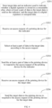
- FIG. 1 is a schematic flowchart of a responding method for a consumable chip according to an embodiment of this application.
- an execution body of this embodiment of this application is a consumable chip, which may be specifically a responding apparatus for a consumable chip.
- the responding apparatus for a consumable chip may be integrated into the consumable chip.
- the consumable chip stores target data and an indicator (indicator) that is used to indicate a type of target data in the consumable chip. At least a part of data in the target data is used as the indicator.
- the target data is a digital signature or unsigned data;
- the responding method for a consumable chip provided in this embodiment includes the following several steps.
- Step 101 Store target data and an indicator used to indicate a type of the target data in the consumable chip, where at least a part of data in the target data is used as the indicator; and the target data is a digital signature or unsigned data.
- the consumable chip may store the digital signature or the unsigned data in a memory.
- the indicator used to indicate that the digital signature is stored in the consumable chip that is, the indicator indicating that the type of the target data is a digital signature is stored, and at least a part of data in the digital signature is used as the indicator indicating that a digital signature is stored.
- the consumable chip stores the unsigned data, in addition to the unsigned data, an indicator indicating that the consumable chip does not store the digital signature is stored, that is, an indicator indicating that the type of the target data is the unsigned data is stored, and at least a part of the unsigned data is used as an indicator indicating that the digital signature is not stored.
- the indicator used to indicate that the digital signature is stored in the consumable chip and the indicator used to indicate that the digital signature is not stored in the consumable chip are indicators used to indicate the type of the target data, and the type of the target data includes the type of the digital signature or the type of the unsigned data.
- the indicator used to indicate the type of the target data in the consumable chip may be one byte (byte) or more bytes of data, or may be one bit (bit) or more bits of data.
- values of the indicator used to indicate that the digital signature is stored in the consumable chip and the indicator used to indicate that the digital signature is not stored in the consumable chip indicate indicators of types of different target data are different. For example, in a consumable chip that stores a digital signature, that is, when it indicates that a type of target data is a digital signature, a value of an indicator is 0x11. In a consumable chip that does not store a digital signature, that is, when it indicates that a type of target data is unsigned data, a value of an indicator is 0x22.
- target data is a digital signature
- a digital signature that is, a digital signature is stored is used to describe an indicator that is used to indicate that a digital signature is stored in a consumable chip and that indicates that the target data is a digital signature.
- FIG. 2 shows a consumable chip including a digital signature and an indicator thereof in the prior art
- the digital signature includes 8 bytes, and is denoted by a hexadecimal digit in the figure.
- the indicator is one byte
- a value in the figure is "11”
- the consumable chip instead of separately storing data used as an indicator, when a printing device requests to access the indicator, the consumable chip selects, from the digital signature, a value "11" that may indicate that the consumable chip stores a digital signature, for example, a seventh byte of the digital signature in FIG. 3 , and send the value to the printing device as a response to the access request.
- Step 102 Receive an access request of a printing device for the indicator.
- the printing device communicates with the consumable chip.
- a specific communication manner is not limited in this embodiment.
- the printing device when the printing device needs to determine whether the consumable chip has digital signature information, if the consumable chip has the digital signature information, the printing device verifies the digital signature to determine authenticity of the consumable chip. If there is no digital signature information in the consumable chip, that is, the consumable chip stores unsigned data, the printing device does not verify the digital signature. Therefore, the printing device sends the access request for the indicator to the consumable chip, and the consumable chip receives the access request for the indicator.
- the printing device may send an access request for a specific address (for example, an address for storing the indicator) to the consumable chip, or may send an access request for continuously accessing multiple addresses, where the multiple addresses may include the address of the indicator. Therefore, the access request sent by the printing device does not necessarily directly indicate that the indicator needs to be accessed.
- the consumable chip may return the value of the indicator when receiving another access request of the printing device.
- Step 103 Select at least a part of data in the target data according to the access request.
- the consumable chip pre-stores the indicator used to indicate the type of the target data in the consumable chip, at least a part of data in the target data is used as the indicator during storage, a storage manner of the indicator in the target data is determined according to the access request, and a corresponding at least a part of data in the target data is selected according to the storage manner of the indicator as the indicator.
- Step 104 Send the at least a part of data to the printing device to respond to the access request of the printing device for the indicator.
- the consumable chip sends at least a part of the target data to the printing device.
- the printing device may learn of the type of the target data in the consumable chip, that is, whether digital signature data is stored. Therefore, the consumable chip may select and send at least a part of data in the target data to the printing device to respond to the access request of the printing device.
- a part of data in the digital signature is used as the indicator, so as to indicate that the consumable chip stores the digital signature.
- the printing device sends the access request, and requires the consumable chip to send an indicator indicating whether the consumable chip includes digital signature information
- the consumable chip sends a part of data in the digital signature to the printing device in response to the access request of the printing device. After obtaining the part of data, the printing device may learn that the consumable chip stores the digital signature data.
- the consumable chip When no digital signature is stored in the consumable chip, the consumable chip stores unsigned data.
- the printing device sends the access request, and requires the consumable chip to send an indicator indicating whether the consumable chip includes digital signature information, that is, an indicator indicating the type of the target data
- the consumable chip responds to the access request of the printing device, and sends at least a part of data in the unsigned data to the printing device. After obtaining the part of data, the printing device learns that there is no digital signature data stored in the consumable chip, and the printing device no longer verifies the data signature.
- target data and an indicator used to indicate a type of the target data in the consumable chip are stored, where at least a part of data in the target data is used as the indicator.
- the target data is a digital signature or unsigned data.
- An access request of a printing device for the indicator is received; at least a part of data in the target data is selected according to the access request; and the at least a part of data is sent to the printing device to respond to the access request of the printing device for the indicator. Because a part of data in the digital signature or the unsigned data represents an indicator of a type of the target data in the chip, there is no need to separately set a storage part to store the indicator and fixedly store a position/address of the indicator. Therefore, when the printing device obtains the indicator of the type of the target data, it is difficult for another third party to learn of a signature status of data in the consumable chip, thereby increasing chip security.
- FIG. 4 is a schematic flowchart of another responding method for a consumable chip according to an embodiment of this application.
- the responding method for a consumable chip provided in this embodiment further refines step 101 on the basis of the responding method for a consumable chip provided in Embodiment 1 of this application, and further includes a step of receiving an access request of a printing device for target data, and sending the target data to the printing device, so as to respond to the access request of the printing device for the target data.
- the responding method for a consumable chip includes the following steps: Step 201: Store target data and an indicator used to indicate a type of the target data in the consumable chip, where at least a part of data in the target data is used as the indicator; and the target data is a digital signature or unsigned data.
- the entire indicator used to indicate the type of the target data in the consumable chip is included in the target data.
- the indicator used to indicate the type of the target data in the consumable chip is data at a fixed address in the target data.
- the indicator may be data at an initial address (the first address) in the digital signature or the unsigned data.
- the consumable chip may fixedly send the data at the initial address of the digital signature or the unsigned data to the printing device.
- the printing device may also not need to separately send an access request for the indicator used to indicate the type of the target data.
- the printing device may directly access these fixed addresses and read the data from these addresses. After the printing device reads the data at these addresses, data that is at specific addresses in these addresses and that is used as the indicator is preset in a control program of the printing device. Therefore, the printing device obtains the data used as the indicator at the address, and further knows whether a digital signature is stored in the consumable chip.
- the printing device does not send an access request for reading the indicator indicating whether the consumable chip includes digital signature information, but the printing device can also find data representing the indicator in the data. In this way, a third party cannot learn of a digital signature status of the consumable chip by collecting a communication process between the printing device and the consumable chip.
- the indicator used to indicate the type of the target data in the consumable chip may be data at multiple different addresses in the target data or common information of data at multiple different addresses.
- data at multiple different addresses in the digital signature or the unsigned data may be separately used as an indicator, and data at these different addresses may have some common information. Therefore, the indicator used to indicate the type of the target data in the consumable chip may be common information of data at multiple different addresses.
- the highest bits of the data at the different addresses in the digital signature are 1, and the highest bits of the data at the different addresses in the unsigned data are 0. It is assumed that when the indicator is "1", it indicates that the digital signature exists, and when the indicator is "0", it indicates that the digital signature does not exist. Therefore, the highest bit may be obtained from any address and used as the indicator.
- the consumable chip When responding to the printing device's request about whether digital signature information is included, the consumable chip randomly selects an address from multiple addresses in the digital signature or the unsigned data, and sends data at the selected address to the printing device. After receiving the data, the printing device determines that the highest bit of the data is 1, indicating that the consumable chip stores a digital signature, and further requests digital signature data of the consumable chip. It is determined that the highest bit of the data is 0, indicating that no digital signature is stored in the consumable chip, and digital signature data of the consumable chip is not requested, or a signature/unsigned data read from the consumable chip is not to be verified.
- the indicator used to indicate the type of the target data in the consumable chip is a combination of data at multiple different addresses in the target data.
- FIG. 5 shows a case in which multiple different addresses in a digital signature are used together as an indicator. Because the highest four bits of the second byte of the digital signature in FIG. 5 are hexadecimal digits 1 and the lowest four bits of the third byte are hexadecimal digits 1, the consumable chip may combine data from these two different bytes together to form a value "11" to respond to an access request of the printing device.
- the indicator used to indicate the type of the target data in the consumable chip is data selected from any address whose value is a preset value in the target data.
- the preset value is first determined, for example, the preset value is "1". Then, a value of the digital signature is determined byte by byte. As shown in FIG. 5 , after the value of the digital signature is determined byte by byte or by using a randomly selected byte, the highest four bits of the second byte of the digital signature are hexadecimal digits 1, which are the preset value "1". Therefore, when it is determined that the value is equal to "1", it is determined that data at this address is selected as the indicator.
- the indicator is obtained by randomly selecting data at any address from the target data.
- a suitable value may be randomly selected from the unsigned data as the indicator in a similar manner, so that a position/address of data used as the indicator does not need to be fixed.
- the value indicating the indicator may be any address in the digital signature or the unsigned data (provided that the value at the address meets a requirement of the indicator, that is, the foregoing preset value), it is difficult for a third party to determine the position of the indicator in the digital signature or the unsigned data, thereby further improving data security.
- At least a part of data in the target data and data outside the target data are jointly used as the indicator of the type of the target data to respond to the access request of the printing device.
- a person skilled in the art may understand that, in addition to the digital signature and the indicator used to indicate that a digital signature is stored in the consumable chip, other data, such as a color, a remaining quantity, a page output (a maximum value of a quantity of pages that can be printed), a quantity of printed pages, a manufacturer, a production date, and a serial number, may be stored in the consumable chip. Therefore, in another embodiment, a part of data in the digital signature and other data than the digital signature are jointly used as the indicator indicating that a digital signature is stored in the consumable chip. When responding to the printing device's request whether digital signature information is included, the consumable chip sends the data outside the digital signature and a part of data in the signature to the printing device.
- the value "11" of the indicator may be formed by using the lowest-four-digit hexadecimal digits 1 of the third byte in the digital signature and the highest-four-digit hexadecimal digits 1 of data "10" other than the digital signature, and the consumable chip extracts a value from these two places and sends the value to the printing device.
- Step 202 Receive an access request of a printing device for the indicator.
- Step 203 Select at least a part of data in the target data according to the access request.
- Step 204 Send the at least a part of data to the printing device to respond to the access request of the printing device for the indicator.
- step 202 to step 204 is the same as an implementation of step 102 to step 104 in Embodiment 1 of this application, and details are not described herein again.
- Step 205 Receive an access request of the printing device for the target data.
- the printing device sends an access request for the digital signature to the consumable chip.
- the printing device learns that there is no digital signature data stored in the consumable chip, the printing device no longer verifies a data signature, but can still obtain the unsigned data from the consumable chip, and the printing device sends an access request for the unsigned data to the consumable chip.
- Step 206 Send the target data to the printing device to respond to the access request of the printing device for the target data.
- the consumable chip obtains the digital signature from a memory of the consumable chip after receiving the access request for the digital signature, and sends the digital signature to the printing device, after receiving data signature data, the printing device verifies the data signature, and after the verification is passed, it indicates that the consumable chip is authentic and trustworthy.
- the printing device may receive the unsigned data, and perform further processing by using the unsigned data.
- At least a part of data in a digital signature or unsigned data indicates an indicator of a type of target data in a consumable chip.
- a storage part does not need to be separately disposed to store the indicator, thereby improving security of the consumable chip.
- the indicator has diversified storage manners, which makes it more difficult for a third party to learn of a digital signature status of the consumable chip, thereby further improving security of the consumable chip.
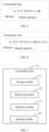
- FIG. 7 is a schematic structural diagram of a consumable chip according to an embodiment of this application.
- the consumable chip 70 provided in this embodiment includes a storage module 71.
- the storage module 71 is configured to store target data and an indicator used to indicate a type of the target data in the consumable chip, where at least a part of data in the target data is used as the indicator; and the target data is a digital signature or unsigned data.
- the consumable chip 70 may further include a receiving module 72, a selection module 73, and a sending module 74, where the receiving module 72 is configured to receive an access request of a printing device, for example, an access request for the indicator.
- the selection module 73 is configured to select at least a part of data in the target data according to the access request.
- the sending module 74 is configured to send the at least a part of data to the printing device in response to the access request of the printing device.
- the consumable chip provided in this embodiment may perform the technical solution of the method embodiment shown in FIG. 1 .
- Implementation principles and technical effects thereof are similar, and are not described herein again.
- the entire indicator used to indicate the type of the target data in the consumable chip is included in the target data.
- the indicator used to indicate the type of the target data in the consumable chip is data at a fixed address in the target data.
- the indicator used to indicate the type of the target data in the consumable chip is data at multiple different addresses in the target data or common information of data at multiple different addresses.
- the indicator used to indicate the type of the target data in the consumable chip is data selected from any address whose value is a preset value in the target data.
- At least a part of data in the target data and data outside the target data are jointly used as the indicator.
- the receiving module 72 is further configured to receive an access request of the printing device for the target data.
- the sending module 74 is further configured to send the target data to the printing device to respond to the access request of the printing device for the target data.
- the consumable chip provided in this embodiment may further perform the technical solution of the method embodiment shown in FIG. 4 .
- Implementation principles and technical effects thereof are similar, and are not described herein again.
- FIG. 8 is a schematic structural diagram of another consumable chip according to an embodiment of this application.
- the consumable chip 80 in this embodiment of this application includes a memory 81, a processor 82, and a computer program.
- the computer program is stored in the memory 81, and is configured to be executed by the processor 82 to implement the responding method for a consumable chip provided in this embodiment of this application.
- the memory 81 and the processor 82 are connected by using a bus.
- the memory may be, but is not limited to, a random access memory (Random Access Memory, RAM), a read only memory (Read Only Memory, ROM), a programmable read-only memory (Programmable Read-Only Memory, PROM), an erasable programmable read-only memory (Erasable Programmable Read-Only Memory, EPROM), an electric erasable programmable read-only memory (Electric Erasable Programmable Read-Only Memory, EEPROM), a flash memory (Flash Memory), or the like.
- the memory is further configured to store a program, and after receiving an execution instruction, the processor executes the program.
- the processor may be an integrated circuit chip and has a signal processing capability.
- the foregoing processor may be a general-purpose processor, including a central processing unit (Central Processing Unit, CPU), a network processor (Network Processor, NP), and the like.
- the processor may be a digital signal processor (DSP), an application-specific integrated circuit (ASIC), a field programmable gate array (FPGA) or another programmable logic device, a discrete-gate or transistor logic device, or a discrete hardware component.
- the processor may implement or perform the methods, the steps, and logical block diagrams that are disclosed in the embodiments of this application.
- the general-purpose processor may be a microprocessor, or the processor may be any conventional processor or the like.
- the consumable chip in this application includes a memory and a processor, the memory is configured to store program instruction code, and the processor is configured to execute the program instruction code, so as to implement the data processing method applied to the consumable chip in the foregoing embodiment.
- An embodiment of this application may be provided as a method, an apparatus, or a computer program product. Therefore, the embodiments of this application may use a form of hardware only embodiments, software only embodiments, or embodiments with a combination of software and hardware.
- the embodiments of this application may use a form of a computer program product that is implemented on one or more computer-usable storage media (including but not limited to a disk memory, a CD-ROM, an optical memory, and the like) that include computer-usable program code.
- a computer-usable storage media including but not limited to a disk memory, a CD-ROM, an optical memory, and the like.
- An embodiment of this application further provides a consumable cartridge, where the consumable cartridge includes a consumable chip, and the consumable chip is detachably mounted on the consumable cartridge.
- the consumable chip is the consumable chip shown in FIG. 7 or FIG. 8 .
- the consumable chip is the consumable chip shown in FIG. 7 or FIG. 8 .
- FIG. 7 or FIG. 8 For related description, refer to the description of the consumable chip shown in FIG. 7 or FIG. 8 . Details are not described herein again.
- the consumable cartridge may be an ink cartridge, a powder cartridge, or a toner cartridge.
- Ink may be accommodated in the ink cartridge
- carbon powder may be accommodated in the powder cartridge or the toner cartridge.
- An embodiment of this application further provides a computer readable storage medium, where a computer program is stored thereon, and the computer program is executed by a processor to implement the responding method for a consumable chip provided in any embodiment of this application.
- An embodiment of this application further provides a chip for running an instruction, where the chip includes a memory and a processor, the memory stores code and data, the memory is coupled to the processor, and the processor runs the code in the memory, so that the chip is configured to perform any responding method for a consumable chip in the foregoing embodiments.
- An embodiment of this application further provides a program product including an instruction.
- the program product includes a computer program.
- the computer program is stored in a computer readable storage medium.
- At least one processor may read the computer program from the computer readable storage medium.
- the at least one processor may implement any responding method for a consumable chip in the foregoing embodiments.
- An embodiment of this application further provides a computer program, and when the computer program is executed by a processor, the computer program is configured to perform any responding method for a consumable chip in the foregoing embodiments.
- These computer program instructions may be provided for a general-purpose computer, a dedicated computer, an embedded processor, or a processor of any other programmable data processing device to generate a machine, so that the instructions executed by a computer or a processor of any other programmable data processing device generate an apparatus for implementing a specific function in one or more processes in the flowcharts and/or in one or more blocks in the block diagrams.
Landscapes
- Engineering & Computer Science (AREA)
- Theoretical Computer Science (AREA)
- Physics & Mathematics (AREA)
- General Physics & Mathematics (AREA)
- Human Computer Interaction (AREA)
- General Engineering & Computer Science (AREA)
- Computer Security & Cryptography (AREA)
- Accessory Devices And Overall Control Thereof (AREA)
- Control Or Security For Electrophotography (AREA)
Applications Claiming Priority (3)
| Application Number | Priority Date | Filing Date | Title |
|---|---|---|---|
| CN201911401975 | 2019-12-31 | ||
| CN202010615229.1A CN111703210B (zh) | 2019-12-31 | 2020-06-30 | 耗材芯片和耗材芯片的响应方法、耗材盒及存储介质 |
| PCT/CN2021/115131 WO2022002283A2 (zh) | 2019-12-31 | 2021-08-27 | 耗材芯片和耗材芯片的响应方法、耗材盒及存储介质 |
Publications (3)
| Publication Number | Publication Date |
|---|---|
| EP4169723A2 true EP4169723A2 (de) | 2023-04-26 |
| EP4169723A4 EP4169723A4 (de) | 2024-02-14 |
| EP4169723B1 EP4169723B1 (de) | 2025-04-23 |
Family
ID=72543878
Family Applications (1)
| Application Number | Title | Priority Date | Filing Date |
|---|---|---|---|
| EP21832471.3A Active EP4169723B1 (de) | 2019-12-31 | 2021-08-27 | Verbrauchschip und antwortverfahren für verbrauchschip, verbrauchskartusche und speichermedium |
Country Status (4)
| Country | Link |
|---|---|
| US (1) | US20230135115A1 (de) |
| EP (1) | EP4169723B1 (de) |
| CN (2) | CN111703210B (de) |
| WO (1) | WO2022002283A2 (de) |
Families Citing this family (2)
| Publication number | Priority date | Publication date | Assignee | Title |
|---|---|---|---|---|
| CN111703210B (zh) * | 2019-12-31 | 2021-07-06 | 珠海艾派克微电子有限公司 | 耗材芯片和耗材芯片的响应方法、耗材盒及存储介质 |
| CN114083913B (zh) * | 2021-11-02 | 2022-09-16 | 珠海艾派克微电子有限公司 | 一种芯片、耗材盒及数据传输方法 |
Family Cites Families (22)
| Publication number | Priority date | Publication date | Assignee | Title |
|---|---|---|---|---|
| JPH04275156A (ja) * | 1991-03-01 | 1992-09-30 | Tokyo Electric Co Ltd | インクジェットプリンタ及びこのプリンタに使用されるインクカートリッジ |
| US5231668A (en) | 1991-07-26 | 1993-07-27 | The United States Of America, As Represented By The Secretary Of Commerce | Digital signature algorithm |
| JPH08310007A (ja) * | 1995-05-19 | 1996-11-26 | Oki Data:Kk | シリアルプリンタ |
| JPH08310071A (ja) * | 1995-05-22 | 1996-11-26 | Graphtec Corp | インクリボンを使用する記録装置 |
| JPH08310070A (ja) * | 1995-05-24 | 1996-11-26 | Nec Eng Ltd | 通帳伝票プリンタ |
| JP3420443B2 (ja) * | 1996-10-17 | 2003-06-23 | キヤノン株式会社 | 画像形成装置及び画像形成方法 |
| TWI341494B (en) * | 2007-02-07 | 2011-05-01 | Mstar Semiconductor Inc | Label paper with rfid function and rfid tag writing apparatus |
| CN102166886B (zh) * | 2011-05-05 | 2013-04-24 | 珠海天威技术开发有限公司 | 耗材芯片及其数据读写方法、耗材容器 |
| CN102231054B (zh) * | 2011-06-08 | 2013-01-02 | 珠海天威技术开发有限公司 | 芯片及芯片数据通信方法、耗材容器、成像设备 |
| CN102950899B (zh) * | 2011-08-26 | 2015-08-05 | 珠海天威技术开发有限公司 | 芯片及其数据写入方法、耗材容器、成像设备 |
| CN102509557B (zh) * | 2011-11-04 | 2014-10-15 | 珠海天威技术开发有限公司 | 电可擦可编程只读存储器的数据擦写控制装置及方法、芯片及其数据写入方法、耗材容器 |
| US10205596B2 (en) * | 2013-07-31 | 2019-02-12 | Hewlett-Pachard Development Company, L.P. | Authenticating a consumable product based on a remaining life value |
| ES2957261T3 (es) * | 2013-07-31 | 2024-01-16 | Hewlett Packard Development Co | Protección de datos en memoria de un producto consumible |
| US9914306B2 (en) * | 2013-07-31 | 2018-03-13 | Hewlett-Packard Development Company, L.P. | Communicating a classification of a consumable product |
| CN105522826B (zh) * | 2014-10-16 | 2017-06-23 | 珠海艾派克微电子有限公司 | 校验值产生方法、耗材芯片和包括该耗材芯片的耗材盒 |
| CN104952485B (zh) * | 2014-11-28 | 2019-07-19 | 珠海艾派克微电子有限公司 | 一种电阻投切电路、存储电路以及耗材芯片 |
| CN104866253B (zh) * | 2015-04-03 | 2018-03-30 | 珠海艾派克微电子有限公司 | 一种芯片及其响应成像装置的方法、成像系统 |
| WO2018054261A1 (zh) * | 2016-09-23 | 2018-03-29 | 珠海艾派克微电子有限公司 | 存储介质、数据处理方法及采用该方法的盒芯片 |
| CN107053854B (zh) * | 2017-01-03 | 2018-10-09 | 珠海艾派克微电子有限公司 | 控制耗材芯片工作的方法、装置、耗材芯片及打印机 |
| CN110271291B (zh) * | 2018-03-16 | 2020-07-07 | 广州众诺电子技术有限公司 | 通用芯片、成像盒、成像系统及使用方法 |
| CN109614060A (zh) * | 2019-01-18 | 2019-04-12 | 珠海艾派克微电子有限公司 | 数据传输方法、装置、耗材芯片及打印耗材 |
| CN111703210B (zh) * | 2019-12-31 | 2021-07-06 | 珠海艾派克微电子有限公司 | 耗材芯片和耗材芯片的响应方法、耗材盒及存储介质 |
-
2020
- 2020-06-30 CN CN202010615229.1A patent/CN111703210B/zh active Active
- 2020-06-30 CN CN202110906869.2A patent/CN113442597B/zh active Active
-
2021
- 2021-08-27 EP EP21832471.3A patent/EP4169723B1/de active Active
- 2021-08-27 WO PCT/CN2021/115131 patent/WO2022002283A2/zh not_active Ceased
-
2022
- 2022-12-29 US US18/148,179 patent/US20230135115A1/en not_active Abandoned
Also Published As
| Publication number | Publication date |
|---|---|
| US20230135115A1 (en) | 2023-05-04 |
| CN111703210B (zh) | 2021-07-06 |
| WO2022002283A3 (zh) | 2022-02-24 |
| EP4169723B1 (de) | 2025-04-23 |
| CN113442597B (zh) | 2022-12-23 |
| CN113442597A (zh) | 2021-09-28 |
| CN111703210A (zh) | 2020-09-25 |
| WO2022002283A2 (zh) | 2022-01-06 |
| EP4169723A4 (de) | 2024-02-14 |
Similar Documents
| Publication | Publication Date | Title |
|---|---|---|
| AU2017268484B2 (en) | Imaging supplies | |
| US20230135115A1 (en) | Consumable chip and consumable chip response method, consumable cartridge, and storage medium | |
| US11176279B2 (en) | Method for identity verification, consumable box and storage medium | |
| US11783023B2 (en) | Digitally signed data | |
| CN110920262B (zh) | 一种耗材芯片及耗材合法性校验方法 | |
| CN111008087B (zh) | 一种消息处理方法及装置 | |
| CN117971874A (zh) | 一种配置字的生成方法、装置、电子设备和存储介质 | |
| CN117632166A (zh) | 文件烧录方法、装置、设备以及存储介质 | |
| US9335695B2 (en) | Imaging device, imaging cartridge, and verification method | |
| US6859847B2 (en) | Parallel electronic architecture comprising a plurality of processing units connected to a communication bus, and addressable by their functional capabilities | |
| CN118092394A (zh) | 访问请求的处理方法、装置、设备及存储介质 | |
| US20240396716A1 (en) | Authentication of logic circuitry packages | |
| CN120234280B (zh) | 寄存器寻址方法、装置、电子设备及存储介质 | |
| CN112527688B (zh) | 页面元素的测试用例处理方法及系统 | |
| CN121246416A (zh) | 耗材芯片识别方法、装置、芯片、设备以及存储介质 | |
| JP2004102897A (ja) | 電子機器 | |
| CN117811698A (zh) | 设备间通信方法、设备、电气系统和存储介质 | |
| CN119562014A (zh) | 数据解密方法、装置、设备以及存储介质 | |
| CN119248340A (zh) | 车辆配置字写入方法、装置、电子设备及存储介质 | |
| CN117785782A (zh) | 基于NVMe 2.0协议的数据检测方法、装置、设备及介质 | |
| KR20250119974A (ko) | 필터링 기반 can 침입 탐지 방법 및 장치 | |
| CN112329046A (zh) | 安全通信方法、装置、电子设备及计算机可读存储介质 | |
| CN119830359A (zh) | 数据完整性的校验方法、芯片以及电子设备 | |
| CN110909056A (zh) | 一种标签数据的查询处理方法、装置、计算机设备和介质 | |
| CN118838725A (zh) | 基于共享内存的通信方法、装置及电子设备 |
Legal Events
| Date | Code | Title | Description |
|---|---|---|---|
| STAA | Information on the status of an ep patent application or granted ep patent |
Free format text: STATUS: THE INTERNATIONAL PUBLICATION HAS BEEN MADE |
|
| PUAI | Public reference made under article 153(3) epc to a published international application that has entered the european phase |
Free format text: ORIGINAL CODE: 0009012 |
|
| STAA | Information on the status of an ep patent application or granted ep patent |
Free format text: STATUS: REQUEST FOR EXAMINATION WAS MADE |
|
| 17P | Request for examination filed |
Effective date: 20230119 |
|
| AK | Designated contracting states |
Kind code of ref document: A2 Designated state(s): AL AT BE BG CH CY CZ DE DK EE ES FI FR GB GR HR HU IE IS IT LI LT LU LV MC MK MT NL NO PL PT RO RS SE SI SK SM TR |
|
| XX | Miscellaneous (additional remarks) |
Free format text: A REQUEST FOR RESTORATION OF THE RIGHT OF PRIORITY BY THE EPO AS DESIGNATED OFFICE HAS BEEN GRANTED (R. 49TER.2 PCT, ART.122 EPC). |
|
| DAV | Request for validation of the european patent (deleted) | ||
| DAX | Request for extension of the european patent (deleted) | ||
| A4 | Supplementary search report drawn up and despatched |
Effective date: 20240116 |
|
| RIC1 | Information provided on ipc code assigned before grant |
Ipc: G06F 21/60 20130101ALI20240110BHEP Ipc: B41J 2/175 20060101AFI20240110BHEP |
|
| GRAP | Despatch of communication of intention to grant a patent |
Free format text: ORIGINAL CODE: EPIDOSNIGR1 |
|
| STAA | Information on the status of an ep patent application or granted ep patent |
Free format text: STATUS: GRANT OF PATENT IS INTENDED |
|
| INTG | Intention to grant announced |
Effective date: 20250109 |
|
| GRAS | Grant fee paid |
Free format text: ORIGINAL CODE: EPIDOSNIGR3 |
|
| GRAA | (expected) grant |
Free format text: ORIGINAL CODE: 0009210 |
|
| STAA | Information on the status of an ep patent application or granted ep patent |
Free format text: STATUS: THE PATENT HAS BEEN GRANTED |
|
| AK | Designated contracting states |
Kind code of ref document: B1 Designated state(s): AL AT BE BG CH CY CZ DE DK EE ES FI FR GB GR HR HU IE IS IT LI LT LU LV MC MK MT NL NO PL PT RO RS SE SI SK SM TR |
|
| REG | Reference to a national code |
Ref country code: GB Ref legal event code: FG4D |
|
| XX | Miscellaneous (additional remarks) |
Free format text: A REQUEST FOR RESTORATION OF THE RIGHT OF PRIORITY BY THE EPO AS DESIGNATED OFFICE HAS BEEN GRANTED (R. 49TER.2 PCT, ART.122 EPC) |
|
| REG | Reference to a national code |
Ref country code: CH Ref legal event code: EP |
|
| REG | Reference to a national code |
Ref country code: DE Ref legal event code: R096 Ref document number: 602021029745 Country of ref document: DE |
|
| REG | Reference to a national code |
Ref country code: IE Ref legal event code: FG4D |
|
| REG | Reference to a national code |
Ref country code: NL Ref legal event code: MP Effective date: 20250423 |
|
| PG25 | Lapsed in a contracting state [announced via postgrant information from national office to epo] |
Ref country code: NL Free format text: LAPSE BECAUSE OF FAILURE TO SUBMIT A TRANSLATION OF THE DESCRIPTION OR TO PAY THE FEE WITHIN THE PRESCRIBED TIME-LIMIT Effective date: 20250423 |
|
| REG | Reference to a national code |
Ref country code: AT Ref legal event code: MK05 Ref document number: 1787429 Country of ref document: AT Kind code of ref document: T Effective date: 20250423 |
|
| PG25 | Lapsed in a contracting state [announced via postgrant information from national office to epo] |
Ref country code: FI Free format text: LAPSE BECAUSE OF FAILURE TO SUBMIT A TRANSLATION OF THE DESCRIPTION OR TO PAY THE FEE WITHIN THE PRESCRIBED TIME-LIMIT Effective date: 20250423 Ref country code: ES Free format text: LAPSE BECAUSE OF FAILURE TO SUBMIT A TRANSLATION OF THE DESCRIPTION OR TO PAY THE FEE WITHIN THE PRESCRIBED TIME-LIMIT Effective date: 20250423 Ref country code: PT Free format text: LAPSE BECAUSE OF FAILURE TO SUBMIT A TRANSLATION OF THE DESCRIPTION OR TO PAY THE FEE WITHIN THE PRESCRIBED TIME-LIMIT Effective date: 20250825 |
|
| PGFP | Annual fee paid to national office [announced via postgrant information from national office to epo] |
Ref country code: DE Payment date: 20250820 Year of fee payment: 5 |
|
| REG | Reference to a national code |
Ref country code: LT Ref legal event code: MG9D |
|
| PG25 | Lapsed in a contracting state [announced via postgrant information from national office to epo] |
Ref country code: NO Free format text: LAPSE BECAUSE OF FAILURE TO SUBMIT A TRANSLATION OF THE DESCRIPTION OR TO PAY THE FEE WITHIN THE PRESCRIBED TIME-LIMIT Effective date: 20250723 Ref country code: GR Free format text: LAPSE BECAUSE OF FAILURE TO SUBMIT A TRANSLATION OF THE DESCRIPTION OR TO PAY THE FEE WITHIN THE PRESCRIBED TIME-LIMIT Effective date: 20250724 |
|
| PG25 | Lapsed in a contracting state [announced via postgrant information from national office to epo] |
Ref country code: PL Free format text: LAPSE BECAUSE OF FAILURE TO SUBMIT A TRANSLATION OF THE DESCRIPTION OR TO PAY THE FEE WITHIN THE PRESCRIBED TIME-LIMIT Effective date: 20250423 |
|
| PG25 | Lapsed in a contracting state [announced via postgrant information from national office to epo] |
Ref country code: BG Free format text: LAPSE BECAUSE OF FAILURE TO SUBMIT A TRANSLATION OF THE DESCRIPTION OR TO PAY THE FEE WITHIN THE PRESCRIBED TIME-LIMIT Effective date: 20250423 |
|
| PGFP | Annual fee paid to national office [announced via postgrant information from national office to epo] |
Ref country code: GB Payment date: 20250820 Year of fee payment: 5 |
|
| PG25 | Lapsed in a contracting state [announced via postgrant information from national office to epo] |
Ref country code: HR Free format text: LAPSE BECAUSE OF FAILURE TO SUBMIT A TRANSLATION OF THE DESCRIPTION OR TO PAY THE FEE WITHIN THE PRESCRIBED TIME-LIMIT Effective date: 20250423 |
|
| PG25 | Lapsed in a contracting state [announced via postgrant information from national office to epo] |
Ref country code: AT Free format text: LAPSE BECAUSE OF FAILURE TO SUBMIT A TRANSLATION OF THE DESCRIPTION OR TO PAY THE FEE WITHIN THE PRESCRIBED TIME-LIMIT Effective date: 20250423 |
|
| PGFP | Annual fee paid to national office [announced via postgrant information from national office to epo] |
Ref country code: FR Payment date: 20250828 Year of fee payment: 5 |
|
| PG25 | Lapsed in a contracting state [announced via postgrant information from national office to epo] |
Ref country code: RS Free format text: LAPSE BECAUSE OF FAILURE TO SUBMIT A TRANSLATION OF THE DESCRIPTION OR TO PAY THE FEE WITHIN THE PRESCRIBED TIME-LIMIT Effective date: 20250723 |
|
| PG25 | Lapsed in a contracting state [announced via postgrant information from national office to epo] |
Ref country code: IS Free format text: LAPSE BECAUSE OF FAILURE TO SUBMIT A TRANSLATION OF THE DESCRIPTION OR TO PAY THE FEE WITHIN THE PRESCRIBED TIME-LIMIT Effective date: 20250823 |
|
| PG25 | Lapsed in a contracting state [announced via postgrant information from national office to epo] |
Ref country code: LV Free format text: LAPSE BECAUSE OF FAILURE TO SUBMIT A TRANSLATION OF THE DESCRIPTION OR TO PAY THE FEE WITHIN THE PRESCRIBED TIME-LIMIT Effective date: 20250423 |
|
| PG25 | Lapsed in a contracting state [announced via postgrant information from national office to epo] |
Ref country code: DK Free format text: LAPSE BECAUSE OF FAILURE TO SUBMIT A TRANSLATION OF THE DESCRIPTION OR TO PAY THE FEE WITHIN THE PRESCRIBED TIME-LIMIT Effective date: 20250423 Ref country code: SM Free format text: LAPSE BECAUSE OF FAILURE TO SUBMIT A TRANSLATION OF THE DESCRIPTION OR TO PAY THE FEE WITHIN THE PRESCRIBED TIME-LIMIT Effective date: 20250423 |
|
| PG25 | Lapsed in a contracting state [announced via postgrant information from national office to epo] |
Ref country code: CZ Free format text: LAPSE BECAUSE OF FAILURE TO SUBMIT A TRANSLATION OF THE DESCRIPTION OR TO PAY THE FEE WITHIN THE PRESCRIBED TIME-LIMIT Effective date: 20250423 |
|
| PG25 | Lapsed in a contracting state [announced via postgrant information from national office to epo] |
Ref country code: EE Free format text: LAPSE BECAUSE OF FAILURE TO SUBMIT A TRANSLATION OF THE DESCRIPTION OR TO PAY THE FEE WITHIN THE PRESCRIBED TIME-LIMIT Effective date: 20250423 |
|
| REG | Reference to a national code |
Ref country code: DE Ref legal event code: R097 Ref document number: 602021029745 Country of ref document: DE |
|
| PG25 | Lapsed in a contracting state [announced via postgrant information from national office to epo] |
Ref country code: SK Free format text: LAPSE BECAUSE OF FAILURE TO SUBMIT A TRANSLATION OF THE DESCRIPTION OR TO PAY THE FEE WITHIN THE PRESCRIBED TIME-LIMIT Effective date: 20250423 |
|
| PG25 | Lapsed in a contracting state [announced via postgrant information from national office to epo] |
Ref country code: IT Free format text: LAPSE BECAUSE OF FAILURE TO SUBMIT A TRANSLATION OF THE DESCRIPTION OR TO PAY THE FEE WITHIN THE PRESCRIBED TIME-LIMIT Effective date: 20250423 |
|
| PG25 | Lapsed in a contracting state [announced via postgrant information from national office to epo] |
Ref country code: RO Free format text: LAPSE BECAUSE OF FAILURE TO SUBMIT A TRANSLATION OF THE DESCRIPTION OR TO PAY THE FEE WITHIN THE PRESCRIBED TIME-LIMIT Effective date: 20250423 |
|
| PLBE | No opposition filed within time limit |
Free format text: ORIGINAL CODE: 0009261 |
|
| STAA | Information on the status of an ep patent application or granted ep patent |
Free format text: STATUS: NO OPPOSITION FILED WITHIN TIME LIMIT |
|
| REG | Reference to a national code |
Ref country code: CH Ref legal event code: L10 Free format text: ST27 STATUS EVENT CODE: U-0-0-L10-L00 (AS PROVIDED BY THE NATIONAL OFFICE) Effective date: 20260304 |
|
| REG | Reference to a national code |
Ref country code: CH Ref legal event code: H13 Free format text: ST27 STATUS EVENT CODE: U-0-0-H10-H13 (AS PROVIDED BY THE NATIONAL OFFICE) Effective date: 20260324 |
|
| PG25 | Lapsed in a contracting state [announced via postgrant information from national office to epo] |
Ref country code: MC Free format text: LAPSE BECAUSE OF FAILURE TO SUBMIT A TRANSLATION OF THE DESCRIPTION OR TO PAY THE FEE WITHIN THE PRESCRIBED TIME-LIMIT Effective date: 20250423 |
|
| 26N | No opposition filed |
Effective date: 20260126 |
|
| PG25 | Lapsed in a contracting state [announced via postgrant information from national office to epo] |
Ref country code: LU Free format text: LAPSE BECAUSE OF NON-PAYMENT OF DUE FEES Effective date: 20250827 |
|
| PG25 | Lapsed in a contracting state [announced via postgrant information from national office to epo] |
Ref country code: CH Free format text: LAPSE BECAUSE OF NON-PAYMENT OF DUE FEES Effective date: 20250831 |