EP4170301B1 - Source de rayonnement infrarouge - Google Patents
Source de rayonnement infrarouge Download PDFInfo
- Publication number
- EP4170301B1 EP4170301B1 EP21204275.8A EP21204275A EP4170301B1 EP 4170301 B1 EP4170301 B1 EP 4170301B1 EP 21204275 A EP21204275 A EP 21204275A EP 4170301 B1 EP4170301 B1 EP 4170301B1
- Authority
- EP
- European Patent Office
- Prior art keywords
- radiation source
- radiation
- optical
- vacuum chamber
- sealed cavity
- Prior art date
- Legal status (The legal status is an assumption and is not a legal conclusion. Google has not performed a legal analysis and makes no representation as to the accuracy of the status listed.)
- Active
Links
Images


Classifications
-
- G—PHYSICS
- G01—MEASURING; TESTING
- G01J—MEASUREMENT OF INTENSITY, VELOCITY, SPECTRAL CONTENT, POLARISATION, PHASE OR PULSE CHARACTERISTICS OF INFRARED, VISIBLE OR ULTRAVIOLET LIGHT; COLORIMETRY; RADIATION PYROMETRY
- G01J3/00—Spectrometry; Spectrophotometry; Monochromators; Measuring colours
- G01J3/02—Details
- G01J3/10—Arrangements of light sources specially adapted for spectrometry or colorimetry
- G01J3/108—Arrangements of light sources specially adapted for spectrometry or colorimetry for measurement in the infrared range
-
- H—ELECTRICITY
- H05—ELECTRIC TECHNIQUES NOT OTHERWISE PROVIDED FOR
- H05B—ELECTRIC HEATING; ELECTRIC LIGHT SOURCES NOT OTHERWISE PROVIDED FOR; CIRCUIT ARRANGEMENTS FOR ELECTRIC LIGHT SOURCES, IN GENERAL
- H05B3/00—Ohmic-resistance heating
- H05B3/40—Heating elements having the shape of rods or tubes
- H05B3/42—Heating elements having the shape of rods or tubes non-flexible
- H05B3/44—Heating elements having the shape of rods or tubes non-flexible heating conductor arranged within rods or tubes of insulating material
-
- G—PHYSICS
- G01—MEASURING; TESTING
- G01N—INVESTIGATING OR ANALYSING MATERIALS BY DETERMINING THEIR CHEMICAL OR PHYSICAL PROPERTIES
- G01N21/00—Investigating or analysing materials by the use of optical means, i.e. using sub-millimetre waves, infrared, visible or ultraviolet light
- G01N21/17—Systems in which incident light is modified in accordance with the properties of the material investigated
- G01N21/1702—Systems in which incident light is modified in accordance with the properties of the material investigated with opto-acoustic detection, e.g. for gases or analysing solids
Definitions
- Embodiments of the present disclosure relate to an IR (infrared) radiation source. More specifically, embodiments relate to an infrared radiation source with filament heating elements in a cavity (vacuum chamber) for providing a highly efficient filament radiation heater. Moreover, embodiments relate to a filament "micro” IR heater (radiation source).
- the sensing of environmental parameters in the ambient atmosphere such as sound, noise, temperature, gases, etc.
- MEMS-based devices gains more and more importance in the implementation of appropriate sensors within mobile devices, home automation, such as smart-home, and the automotive sector.
- PAS photoacoustic spectroscopy
- planar, non-insulated radiators are generally used for generating the required excitation lines.
- only a small amount of the electrical power is transferred into the emitted optical power (optical energy).
- a further application case is a radiation heater used for inducing thermal phase transitions in phase transition materials, such as GeSbTe (GST).
- GST GeSbTe
- a radiation heater used for inducing thermal phase transitions in phase transition materials, such as GeSbTe (GST).
- GST GeSbTe
- a tungsten heater is used which is in direct contact to the material. This has a negative impact on the potentially achievable cooling rate and, thus, on the amorphization of the GST material.
- WO 2016/145127 A1 relates to mid-infrared (MIR) hyperspectral spectroscopy systems and method thereof.
- the MIR spectroscopy systems comprise a hierarchical spectral dispersion.
- the hierarchical spectral dispersion is derived by employing at least two diffractive lens arrays, located on either side of a test sample, each receiving input radiation having an input spectral range and distributing the input radiation into a plurality of output signals, each having a fraction of the spectral range of the input radiation.
- the signal multiplication factor of the two arrays is multiplied in a manner that mitigates the propagation of wavelength harmonics through the system.
- US 3,443,144 A relates to an infrared incandescent lamp.
- the infrared incandescent electric lamps have an oval-shaped quartz envelope, with two parallel tungsten filaments, extending the length of the lamp, and are mounted within said envelope.
- XP 000 271 784 relates to electrical and optical characteristics of vacuum-sealed polysilicon microlamps.
- the silicon-filament vacuum-sealed incandescent light source has been fabricated using IC technology and subsurface micromachining.
- the incandescent source consists of a heavily doped p+ polysilicon filament coated with silicon nitride and enclosed in a vacuum-sealed cavity in the siliconchip surface.
- the filament is formed beneath the surface and later released using sacrificial etching to obtain a microstructure that is protected from the external environment.
- the filament is electrically heated to reach incandescence at a temperature near 1400 K.
- an IR (infrared) radiation source comprises the features according to claim 1.
- the IR radiation source with filament heating elements in a vacuum chamber an increased efficiency can be achieved when compared to current IR radiation sources, wherein the IR radiation source according to the embodiments can be manufactured as an integrated application on a wafer, e.g. a Si wafer, wherein the manufacturing process is in principle CMOS compatible.
- the suggested filament radiation heater comprises a high radiation yield when compared to the electrical power used, resulting in an increased efficiency.
- the utilization of the suggested filament radiation heater allows a faster cooling rate of the material since the heat source and the GST material are spatially separated (spaced).
- lateral means a direction parallel to the x- and/or y-direction or a direction parallel to the x-y-plane, wherein the term “vertical” means a direction parallel to the z-direction.
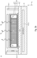
- Fig. 1 shows a schematic cross-sectional view of an IR (infrared) radiation source 10 according to an embodiment.
- the IR radiation source 10 comprises a sealed cavity structure 20, e.g. in form of an encapsulation structure, enclosing a vacuum chamber 22 having low atmospheric pressure, e.g. a low internal atmospheric pressure, such as a near vacuum condition.
- the sealed cavity structure comprises a thermally and electrically insulating material 24, 26 or a corresponding material combination for enclosing, such as encapsulating and sealing, the vacuum chamber 22.
- the IR radiation source 10 further comprises a plurality of heating filaments 30 extending in the vacuum chamber 22 between opposing electrode regions 32, 34 at opposing wall regions 22-1, 22-2 of the vacuum chamber 22.
- the heating filaments 30 are electrically connected in parallel, wherein the heating filaments 30 and the electrode regions 32, 34 have a highly electrically conductive material.
- the IR radiation source 10 further comprises an optical isolation structure 40 adjacent to the vacuum chamber 22 (and the sealed cavity structure 20) for optically confining the IR radiation and providing a predominant propagation direction of the IR radiation 50.
- the optical isolation structure 40 may be arranged adjacent (e.g. parallel) to at least one, to a plurality or to all side wall regions 22-1, ... 22-6, for example, of the vacuum chamber 22 for optically confining the IR radiation 50 generated by the IR radiation source 10 in an activated condition, i.e. in an energized condition of the heating filaments 30, and for providing a predominant propagation direction of the IR radiation 50 in the sealed cavity structure 20 and for providing a predominant emission direction of the IR radiation 50 from the sealed cavity structure 20.
- the vacuum chamber 22 comprises a rectangular footprint
- the sealed cavity structure 20 and the vacuum chamber 22 may be regarded, for example, as a rectangular parallelepiped or cuboid having three pairs of opposing side faces or side wall regions 22-1, ... 22-6.
- the opposing side wall regions 22-1, 22-2 extend parallel to the x-y-plane
- the opposing side wall regions 22-3, 22-4 extend parallel to the y-z-plane
- the opposing side wall regions 22-5, 22-6 extend parallel to the x-z-plane.
- the vacuum chamber 22 may comprise a rectangular, square, circular, elliptic, etc. footprint shape and comprises the correspondingly shaped side wall regions, wherein the heating filaments 30 are enclosed in sealed cavity structure 22.
- the further reflector elements 40-1a, ..., 40-6, as optionally shown in Fig. 1 are only shown for illustrating the different implementation options of the optical isolation structure 40, wherein the different isolation elements of the optical isolation structure 40-1a, ... , 40-6 are described below in more detail.
- the optical isolation structure may comprise (at least) one, a plurality or all reflector elements 40-1a, ..., 40-6 (as shown in Fig. 1 ) for optically confining and/or directing the IR radiation 50.
- the reflector element 40-1a may be formed as a cavity (optical reflector) in the insulating material layer 24 and is arranged adjacent and parallel to the first side wall region 22-1 of the vacuum chamber 22.
- the reflector element 40-1b may be formed as a metallization layer (optical reflector) on the insulating material layer 24 and is arranged adjacent and parallel to the first side wall region 22-1 of the vacuum chamber 22.
- the reflector element 40-2a may be formed as a cavity (optical reflector) in the substrate 70 (or in the insulating material layer 24) and is arranged adjacent and parallel to the second side wall region 22-2 of the vacuum chamber 22.
- the reflector element 40-2b may be formed as a metallization layer (optical reflector) on the substrate 70 or in the insulating material layer 24 and is arranged adjacent and parallel to the second side wall region 22-2 of the vacuum chamber 22.
- the reflector element 40-3 may be formed as a trench (optical reflector) in the insulating material layer 24 and is arranged adjacent and parallel (or inclined) to the third side wall region 22-3 of the vacuum chamber 22.
- the reflector element 40-4 may be formed as a trench (optical reflector) in the insulating material layer 24 and is arranged adjacent and inclined (or parallel) to the fourth side wall region 22-4 of the vacuum chamber 22.
- the reflector element 40-5 may be formed as a trench (optical reflector) in the insulating material layer 24 and is arranged adjacent and parallel to the fifth side wall region 22-5 (parallel to the x-z-plane - see for example Fig. 2a-d ) of the vacuum chamber 22.
- the reflector element 40-6 (see for example Fig. 2a-d ) may be formed as a trench (optical reflector) in the insulating material layer 24 and is arranged adjacent and parallel to the sixth side wall region 22-6 (parallel to the x-z-plane - see for example Fig. 2a-d ) of the vacuum chamber 22.
- the optical isolation structure 40 may comprise at least one of the cavities 40-1a, 40-2a, of the trenches 40-3, 40-4, 40-5, 40-6, and/or of the metal films 40-1b, 40-2b for defining the optical path of the generated IR radiation 50.
- the IR radiation source 10 further comprises contact pads 60 and vias 62 for electrically connecting the top-electrode region 32 and comprises the contact pad 64 and the via 66 for contacting the opposing electrode region 34 (at opposing wall regions of the vacuum chamber 22).
- the contact pads 60, 64 may be provided for an external connectivity of the IR radiation source 10.
- the contact pads 60, 64 may be arrange in the same plane as the metallization layer 40-1b.
- the IR radiation source 10 may be arranged on a substrate 70, wherein the substrate 70 may comprise a semiconductor material, such as silicon, or a glass material, etc.
- the present concept for implementing the IR radiation source 10 results in a high efficient radiation heater 10 by using the heating filaments 30 of a material with a high melting point, wherein the material may comprise or consist of carbon, graphene, polysilicon or tungsten, for example.
- the arrangement of the heating filaments 30 in the vacuum chamber 22 of the sealed cavity structure 20 provides a thermal isolation of the heating filaments 30.
- the material for the heating filaments 30 and the opposing electrode regions 32, 34 (top and bottom electrodes) is highly electrically conducting and may be chosen to be transparent for the generated IR radiation in the energized condition of the heating filaments 30.
- the IR radiation source 10 using the plurality of heating filaments 30 allows the utilization of different materials for the heating elements 30, i.e. the heating filaments 30, between the opposing electrode regions 32, 34, resulting in an optimization of the characteristics of the IR radiation source 10.
- the emission spectrum of the IR radiation source 10 may be optimized based on the same material used for the heating filaments 30 and the opposing electrode regions 32, 34.
- a high light intensity (IR radiation intensity) at a reduced chip area can be achieved by the IR radiation heater 10 when compared to state of the art infrared heaters.
- the modular layout of the IR radiation source 10 according to the embodiments is easy to adapt to specific applications, e.g. to PAS or GST applications.
- the manufacturing process of the IR radiation source 10 is easily integratable in a CMOS manufacturing process flow.
- current CMOS manufacturing processes allow to achieve a high mechanical stability, a high temperature homogeneity and a high vacuum stability of the IR radiation source 10.
- the IR radiation source 10 provides a broad-band IR source with a high opto-electrical efficiency. Further, the structure and setup of the IR radiation source 10 allows to implement a manufacturing process which is compatible with current CMOS process flows.
- the vertical current flow through the heating filaments 30 which have a high aspect ratio and are arranged in an electrical parallel connection by means of the top and bottom plate electrodes 32, 34, respectively, results in a compact device 10 with a high radiation density at a (relatively) low operating voltage.
- the materials for the heating filaments 30 may be selectively chosen to comprise a high melting point, a sufficient electrical conductivity, a CMOS process compatibility, and the possibility of having a high aspect ratio deposition.
- Exemplary materials for the heating filaments 30 are, for example, carbon, graphene, polysilicon or tungsten. The above indicated materials are suited for this application due their high melting point, low expansion coefficient and sufficient (high) conductivity, and their technological manufacturability in high aspect ratios and different/various geometries.
- an insulating material such as silicon nitride (Si 3 N 4 ) or titanium nitride (TiN) may be used, for example. These materials have a large band gap and a low thermal conductivity. Furthermore, these materials have a high density to (long-term) prevent hydrogen or oxygen diffusion into the vacuum chamber 22. Furthermore, these materials have a low thermal expansion coefficient and are compatible to CMOS process flows.
- the optical isolation structure 40 (with at least one reflection element 40-#) may form a light pipe for confining the generated IR radiation 50 and providing a predominant propagation direction and emission direction of the generated IR radiation 50.
- the optical isolation structure 40 may comprise at least one or a plurality of trenches, cavities and/or metal films for defining the optical path of the generated IR radiation 50.
- the IR radiation source 10 which is implemented according to the different embodiments, uses the fact that the radiation yield increases by T 4 (Boltzmann Law), so that a material for the heating filaments 30 having a high melting point (temperature of destruction) contributes to a high IR radiation yield.
- the IR radiation emission of the heating filaments 30 is generated by the interaction between the current flow (electrons) through the heating filaments 30 and the material of the heating filaments 30.
- a high current flow and a corresponding geometry in form of the heating filaments 30 favors and supports the IR radiation emission of the IR radiation source 10.
- a relatively low temperature i.e. a temperature as low as possible
- the connection area i.e. at the opposing electrode regions 32, 34, may be achieved by the utilization of a highly electrically conductive material, e.g. with a specific electrical resistance (electrical resistivity) below 5 mOhm cm.
- the efficiency of the IR radiation source 10 is further increased as the annealing or glowing region, i.e. the vacuum chamber 22, loses a very small amount of energy due to a very low heat conduction and heat convection to adjacent regions or the environment.
- the IR radiation source 10 allows due to its specific structure that essentially all or at least a predominant amount of the generated IR radiation is used and consumed for the intended utilization of providing and emitting the IR radiation 50 (and is not emitted and radiated in an unused way).
- the IR radiation source 10 allows for a high thermal stability and a manageable technological manufacturability.
- the emitted radiation amount (radiation portion) is at high temperatures (red to yellow glowing heating elements 30) very high and can be directed and bundled by the optical isolation structure 40, such as by means of the optical reflectors 40-# and optional further optical elements, such as lenses.
- the usable energy of the IR radiation source 10 is increased due to the reduced convection and heat conduction to adjacent regions.
- the emitted radiation is minimally absorbed by materials (substances) outside the intended energy flow, thus resulting in reduced (low) convection losses.
- the present heater system in form of the IR radiation source 10 achieves a high system inertia, which results in a high threshold frequency (cut-off frequency) for on- and off-switching operations.
- the heating filaments 30 and the electrode regions 32, 34 comprise the same highly electrically conductive material having a melting temperature or melting point higher than 1000°, 2000° or 3500° Celsius.
- the conductive material of the heating filaments may comprise carbon, graphene, polysilicon or tungsten for providing the high annealing (soak) temperature.
- the opposing electrode regions 32, 34 of the heating filaments 30 are formed as plate electrodes.
- the heating filaments may have a length (between the opposing electrode regions) between 0.1 and 80 ⁇ m (or between 2 and 200 ⁇ m) and have an aspect ratio (diameter to depth) of 1:1 up to 1:80. This corresponds to a thickness of the filaments 30 of about 1nm to 1 ⁇ m.
- the spacing between the filaments 30 is in the range between 10 nm and 1 ⁇ m.
- the insulator material of the sealed cavity structure 20 is optically transparent to the IR radiation 50, i.e. for the radiation 50 generated by the heating filament(s) 30 in an excitation condition in the vacuum chamber 22.
- the insulating material 24, 26 of the sealed cavity structure 20 comprises a first insulating layer 24 having a silicon nitride material enclosing the vacuum chamber 22 of the sealed cavity structure 20.
- the first layer 24 may have a thickness of at least 0,3 ⁇ m, e.g. between 0.3 and 1 ⁇ m.
- the insulating material 24, 26 of the sealed cavity structure 20 further comprises a second insulating layer 26 comprising a silicon dioxide material for enclosing the first layer 24.
- the second layer 26 may have a thickness of at least 1 ⁇ m, e.g. between 1 and 3 ⁇ m.
- the insulating material 24, 26 of the sealed cavity structure 20 further comprises a third insulating layer 28, e.g. a passivation layer, comprising a titanium nitride material.
- the third layer may have a thickness between 0.1 and 0.3 ⁇ m, e.g. about 200 nanometers.
- the thermal isolation of the vacuum chamber 22 and of the heating filaments 30 which are arranged therein is achieved by a silicon oxide housing having a thickness of at least 1 ⁇ m.
- the low atmospheric pressure in the vacuum chamber 22 comprises a cavity pressure less than 3 mbar (2.25 Torr or 300 Pa) or less than 1 mbar (0.75 Torr or 100 Pa).
- the vacuum in the vacuum chamber 22 may be in a range of 1 mbar or below and long-term stable. This can be achieved by the SiN encapsulation, wherein the SiN material (having a thickness of roughly 200 nm) is a diffusion barrier, even for hydrogen.
- the vacuum chamber may comprise a reduced low atmospheric pressure (vacuum or near vacuum) with an atmospheric pressure of about or below 3 mbar or 1 mbar.
- the internal atmospheric pressure in the cavity chamber may, therefore, be in a range between 3 mbar and 0.1 mbar.
- the reduced atmospheric pressure in the vacuum chamber 22 may be achieved based on the process pressure during the position of the different layers for forming the sealed cavity structure 20 and sealing the vacuum chamber 22, such that the cavity chamber has said reduced atmospheric pressure.
- the optical isolation structure 40 forms an optical waveguide structure for providing an optical path with the predominant propagation direction of the IR radiation 50 in the sealed cavity structure 20.
- the optical isolation structure may comprise optical reflector elements 40-# for providing the optical path for the IR radiation 50 in the sealed cavity structure 20.
- the optical reflector elements 40-# of the optical isolation structure 40 comprise a metallization layer adjacent to the side wall region of the sealed cavity structure 20, and/or the optical reflector elements 40-# of the optical isolation structure 40 may comprise a cavity in the substrate 70 or a trench in the insulating material 24, 26 of the sealed cavity structure 20 or adjacent to the sealed cavity structure 20.
- the sealed cavity structure 40 i.e. at least on optical reflector element 40-# of the optical isolation structure 40, is arranged on the substrate 70, wherein the optical isolation structure 40 may be formed as a metallization layer on a surface region 70-A of the substrate 70 adjacent to a side wall region of the sealed cavity structure 20. Additionally or alternatively, the optical isolation structure 40, i.e. at least one optical reflector element 40-# of the optical isolation structure 40, may be formed as a cavity in the substrate 70 adjacent to the side wall region of the sealed cavity structure 20.
- SON silicon on nothing
- the cavities of the optical isolation structure 40 may comprise a thickness of about 0.3 - 1 ⁇ m, wherein the trenches of the optical isolation structure 40 comprise a width of about 0.1 - 0.5 ⁇ m.
- the IR radiation source 10 may further comprise an optical element 40-# for guiding the IR radiation 50, wherein the optical element 40-# comprises a lens and/or prism-element at an radiation output area (radiation outlet) of the sealed cavity structure 20.
- the radiator cavity 22 itself is enclosed by optical isolation structures, such as cavities (with a thickness of 0.1 to 1 ⁇ m) and trenches (with a width of 0.1 to 0.5 ⁇ m) in the surrounding silicon oxide layers 26 and/or in the substrate 70, such as a semiconductor wafer, except for the intended radiation output location and radiation emission direction.
- optical isolation structures such as cavities (with a thickness of 0.1 to 1 ⁇ m) and trenches (with a width of 0.1 to 0.5 ⁇ m) in the surrounding silicon oxide layers 26 and/or in the substrate 70, such as a semiconductor wafer, except for the intended radiation output location and radiation emission direction.
- the specific arrangement of the optical isolation structure 40 forms a kind of an optical waveguide structure for providing an optical path with a predominant propagation direction of the IR radiation in the sealed cavity structure and a predominant emission direction of the generated IR radiation from the IR radiation source 10.
- the optical isolation structure 40 may comprise at least or a plurality of trenches, cavities and/or metal films for defining the optical path of the generated IR radiation 50.
- an optical isolation of the generated IR radiation may be achieved by the IR radiation source according to the embodiments described herein.
- the heating filaments 30 may be arranged as a rectangular mxn array in a square or rectangular vacuum chamber 22, i.e. in a vacuum chamber 22 having a square or rectangular footprint parallel to the x-y-plane.
- the top and bottom electrode contacts 62, 66 are arranged at diagonally opposing portions of the electrode regions 32, 34.
- the reflector elements 40-3, 40-4 may be formed as optical reflectors adjacent and parallel to the third and fourth side wall regions 22-3, 22-4 of the vacuum chamber 22.
- the reflector elements 40-5, 40-6 may be formed as optical reflectors adjacent and parallel to the fifth and sixth side wall regions 22-5, 22-6 of the vacuum chamber 22.
- the heating filaments 30 may be arranged as a rectangular 2xn array in a square or rectangular vacuum chamber 22, i.e. in a vacuum chamber 22 having a rectangular footprint parallel to the x-y-plane.
- the top and bottom electrode contacts 62, 66 are arranged at opposing portions of the electrode regions 32, 34.
- the reflector elements 40-3, 40-4 may be formed as optical reflectors adjacent and parallel to the third and fourth side wall regions 22-3, 22-4 of the vacuum chamber 22.
- the reflector elements 40-5, 40-6 may be formed as optical reflectors adjacent and parallel to the fifth and sixth side wall regions 22-5, 22-6 of the vacuum chamber 22.
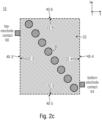
- the heating filaments 30 may be arranged in a line arrangement in a square or rectangular vacuum chamber 22, i.e. in a vacuum chamber 22, having a square or rectangular footprint parallel to the x-y-plane.
- the top and bottom electrode contacts 62, 66 are arranged at diagonally opposing portions of the electrode regions 32, 34.
- the reflector elements 40-3, 40-4 may be formed as optical reflectors adjacent and parallel to the third and fourth side wall regions 22-3, 22-4 of the vacuum chamber 22.
- the reflector elements 40-5, 40-6 may be formed as optical reflectors adjacent and parallel to the fifth and sixth side wall regions 22-5, 22-6 of the vacuum chamber 22.
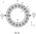
- the heating filaments 30 may be arranged in a circular arrangement in a circular vacuum chamber 22, i.e. in a vacuum chamber 22, having a circular footprint parallel to the x-y-plane.
- the top and bottom electrode contacts 62, 66 are arranged at opposing portions of the electrode regions 32, 34.
- the reflector elements 40-1, 40-2 may be formed as optical reflectors adjacent and parallel to the first and second side wall regions 22-1, 22-2 of the vacuum chamber 22.
- the shape of the vacuum chamber 22 and the geometrical arrangement or alignment of the heating filaments 30 therein includes a large number of different implementations, wherein the implementations as shown Figs. 2a-d for the vacuum chamber 22 and the heating filaments 30 is not to be regarded as exhaustive.
- the shape (footprint) of the vacuum chamber 22 may also comprise one of a circular, square, oval and ellipse shape (or any convex polygon shape), for example.
- the IR radiation source 10 may comprise the (laterally extending) optical reflector elements 40-1a, 40-2a, wherein the vacuum chamber 22 with the heating filaments 30 is sandwiched between the optical reflector elements 40-1a, 40-2a, and further comprises the (vertically extending) optical reflector element (trench) 40-3 which is laterally arranged to the vacuum chamber 22.
- the IR radiation source 10 may further comprise the (vertically extending) optical reflector elements 40-5, 40-6, wherein the vacuum chamber 22 with the heating filaments 30 is sandwiched between the optical reflector elements 40-5, 40-6.
- the resulting emission direction of the generated IR radiation is lateral (in parallel to the x direction) of the IR radiation source 10.
- the IR radiation source 10 may comprise the (laterally extending) optical reflector element 40-2a, and further comprises the (vertically extending) optical reflector elements (trenches) 40-3, 40-4 which are laterally arranged to the vacuum chamber 22, wherein the vacuum chamber 22 with the heating filaments 30 is sandwiched between the optical reflector elements 40-3, 40-4.
- the IR radiation source 10 may further comprise the (vertically extending) optical reflector elements 40-5, 40-6, wherein the vacuum chamber 22 with the heating filaments 30 is sandwiched between the optical reflector elements 40-5, 40-6.
- the resulting emission direction of the generated IR radiation is vertical (in parallel to the z direction) of the IR radiation source 10.
- the IR radiation source 10 may comprise the (laterally extending) optical reflector elements 40-1, 40-2, wherein the vacuum chamber 22 with the heating filaments 30 is sandwiched between the optical reflector elements 40-1, 40-2, and further comprises the (vertically extending) optical reflector elements (trenches) 40-3, 40-4 which are laterally arranged to the vacuum chamber 22.
- the optical reflector element (trench) 40-3 is arranged parallel to the y-z-plane, wherein the optical reflector element (trench) 40-4 is arranged with an inclined angle, e.g. 45° (e.g. between 30 and 60°) with respect to the x-y-plane.
- the IR radiation source 10 may further comprise the (vertically extending) optical reflector elements 40-5, 40-6, wherein the vacuum chamber 22 with the heating filaments 30 is sandwiched between the optical reflector elements 40-5, 40-6.
- the resulting emission direction of the generated IR radiation is lateral (in parallel to the z direction) of the IR radiation source 10.
- the IR radiation source 10 may comprise the (laterally extending) optical reflector elements 40-1, 40-2, wherein the vacuum chamber 22 with the heating filaments 30 is sandwiched between the optical reflector elements 40-1, 40-2, and further comprises the optical reflector elements (trenches) 40-3, 40-4 which are laterally arranged to the vacuum chamber 22 and are arranged with an inclined angle, e.g. 45° (e.g. between 30 and 60°) with respect to the x-y-plane.
- the IR radiation source 10 may further comprise the (vertically extending) optical reflector elements 40-5, 40-6, wherein the vacuum chamber 22 with the heating filaments 30 is sandwiched between the optical reflector elements 40-5, 40-6.
- the resulting emission direction of the generated IR radiation is lateral (in parallel to the z direction) of the IR radiation source 10.
- optical reflector elements in form of cavities and the vertically or inclined extending optical reflector elements in form of trenches, it is pointed out to the fact that at least one, a plurality or all of these optical reflector elements are also formable by means of reflective metallic layers.
- the IR radiation source 10 comprises heating filaments 30 which are arranged and sealed in a vacuum chamber 22, wherein the material of the heating filaments 30 comprises at least the conductivity of highly doped polysilicon.
- the material for the heating filaments may, for example, comprise carbon, graphene, polysilicon or tungsten or other suitable highly conductive, CMOS process flow compatible materials.
- the heating filaments 30 may be manufactured in high aspect ratios between large area electrodes (plate electrodes with a narrow alignment of the heating filaments, wherein the electrodes and heating filaments are homogeneously connected.
- a low expansion coefficient of the material of the heating filaments 30 supports the mechanical stability of the IR radiation source 10, wherein the heating filaments 30 comprise an elastic material which is stable in the case of vibrations.
- the high melting temperature of the filament material provides for a high radiation yield, especially due to the low atmospheric pressure (near vacuum) in the vacuum chamber.
- the low atmospheric pressure in the vacuum chamber 22 also provides for an energy optimization of the radiator source 10.
- the vacuum chamber 22 (cavity) having the low atmospheric pressure (good vacuum) fits to the manufacturing of the heat elements, e.g. by etching an SiO sacrificial layer by means of HF (hydrofluoric acid) and a sealing, e.g. as sputter sealing, under vacuum. Further, carbon has a good etching selectivity to HF.
- the housing of the vacuum chamber 22 comprises a SiN/TiN... barrier against H2, O2, etc.
- This insulator combination provides a device passivation with a final furnace anneal.
- the thermal isolation of the vacuum chamber 22 may be achieved by housing the vacuum chamber 22 into thick SiO layers.
- the optical isolation structure forms an optical waveguide structure for providing an optical path with a predominant propagation direction of the IR radiation in the sealed cavity structure and a predominant emission direction from the IR radiation source.
- waveguide materials and optical elements such as lenses, prisms, etc., can be used to provide a localized radiation output.
- an IR (infrared) radiation source comprises a sealed cavity structure enclosing a vacuum chamber having a low atmospheric pressure, wherein the sealed cavity structure comprises a thermally and electrically insulating material for enclosing the vacuum chamber, a plurality of heating filaments extending in the vacuum chamber between opposing electrode regions at opposing wall regions of the vacuum chamber, wherein the heating filaments are electrically connected in parallel, and wherein the heating filaments and the electrode regions have a highly electrically conductive material, and an optical isolation structure adjacent to the vacuum chamber for optically confining the IR radiation and providing a predominant propagation direction of the IR radiation.
- the heating filaments and the electrode regions comprise the same highly electrically conductive material having a melting temperature higher than 1000° Celsius.
- the conductive material of the heating filaments comprises carbon, graphene, polysilicon or tungsten.
- the opposing electrode regions of the heating filaments are formed as planar electrodes.
- the heating filaments have a length between 0.1 and 80 micrometers and have an aspect ratio of 1:1 up to 1:80.
- the insulator material of the sealed cavity structure is optically transparent to the IR radiation.
- the insulating material of the sealed cavity structure comprises a first insulating layer having a silicon nitride material enclosing the vacuum chamber of the sealed cavity structure, and wherein the insulating material of the sealed cavity structure further comprises a second insulating layer comprising a silicon dioxide material for enclosing the first layer.
- the insulating material of the sealed cavity structure further comprises a third insulating layer comprising a titanium nitride material.
- the low atmospheric pressure in the vacuum chamber comprises a cavity pressure less than 3 mbar (2.25 Torr or 300 Pa) or less than 1 mbar (0.75 Torr or 100 Pa).
- the optical isolation structure forms an optical waveguide structure for providing an optical path with the predominant propagation direction of the IR radiation in the sealed cavity structure.
- the optical isolation structure comprises optical reflector elements for providing the optical path for the IR radiation.
- the optical reflector elements of the optical isolation structure comprise a metallization layer adjacent to the side wall region of the sealed cavity structure, or wherein the optical reflector elements of the optical isolation structure comprise a cavity in a substrate or a trench in the insulating material adjacent to the sealed cavity structure.
- the sealed cavity structure is arranged on a substrate, wherein the optical isolation structure is formed as a metallization layer on a surface region of the substrate adjacent to a side wall region of the sealed cavity structure, or wherein the optical isolation structure is formed as a cavity in the substrate adjacent to the side wall region of the sealed cavity structure.
- the cavities of the optical isolation structure comprise a thickness of about 0.3 - 1 ⁇ m and/or wherein the trenches of the optical isolation structure comprise a width of about 0.1 - 0.5 ⁇ m.
- the IR radiation source further comprises an optical element for guiding the IR radiation, wherein the optical element comprises a lens and/or prism-element at an radiation output area of the sealed cavity structure.
Landscapes
- Physics & Mathematics (AREA)
- Spectroscopy & Molecular Physics (AREA)
- General Physics & Mathematics (AREA)
- General Health & Medical Sciences (AREA)
- Analytical Chemistry (AREA)
- Biochemistry (AREA)
- Chemical & Material Sciences (AREA)
- Life Sciences & Earth Sciences (AREA)
- Immunology (AREA)
- Pathology (AREA)
- Health & Medical Sciences (AREA)
- Resistance Heating (AREA)
- Micromachines (AREA)
- Physical Vapour Deposition (AREA)
Claims (15)
- Source (10) de rayonnement IR (infrarouge) comprenant :une structure (20) de cavité scellée enfermant une chambre (22) à vide ayant une basse pression atmosphérique, dans laquelle la structure (20) de cavité scellée comprend un matériau (24, 26) isolant thermiquement et électriquement pour enfermer la chambre (22) à vide,des électrodes (32, 34) opposées en plaque,une pluralité de filaments (30) chauffants s'étendant verticalement dans la chambre (22) à vide entre les électrodes (32, 24) opposées en plaque en des régions (22-1, 22-2) opposées de parois de la chambre à vide, dans laquelle les filaments (30) chauffants sont montés électriquement en parallèle, et dans laquelle les filaments (30) chauffants et les électrodes (32, 24) en plaque ont un matériau très conducteur de l'électricité, etune structure (40) d'isolation optique contigüe à la chambre (22) à vide pour confiner optiquement le rayonnement (50) IR et donner une direction de propagation prépondérante du rayonnement (50) IR.
- La source (10) de rayonnement IR de la revendication 1, dans laquelle les filaments (30) chauffants et les électrodes (32, 34) en plaque comprennent le même matériau très conducteur de l'électricité ayant un point de fusion plus haut que 1000° Celsius.
- La source (10) de rayonnement IR de la revendication 1 ou 2, dans laquelle le matériau conducteur des filaments (30) chauffants comprend du carbone ou du graphène.
- La source (10) de rayonnement IR de l'une quelconque des revendications précédentes, dans laquelle le matériau conducteur des filaments (30) chauffants comprend du polysilicium ou du tungstène.
- La source (10) de rayonnement IR de l'une quelconque des revendications précédentes, dans laquelle les filaments (30) chauffants ont une longueur comprise entre 0,1 et 80 microns et ont un rapport d'aspect de 1:1 allant jusqu'à 1:80.
- La source (10) de rayonnement IR de l'une quelconque des revendications précédentes, dans laquelle le matériau isolant de la structure (20) de cavité scellée est transparent optiquement au rayonnement (50) IR.
- La source (10) de rayonnement IR de l'une quelconque des revendications précédentes, dans laquelle le matériau isolant de la structure (20) de cavité scellée comprend une première couche (24) isolante ayant un matériau en nitrure de silicium enfermant la chambre (22) à vide de la structure (20) de cavité scellée, et
dans laquelle le matériau isolant de la structure (20) de cavité scellée comprend en outre une deuxième couche (26) isolante comprenant un matériau en dioxyde de silicium pour enfermer la première couche (24). - La source (10) de rayonnement IR de l'une quelconque des revendications précédentes, dans laquelle le matériau (24, 26) isolant de la structure (20) de cavité scellée comprend une troisième couche (28) isolante comprenant un matériau en nitrure de titane.
- La source (10) de rayonnement IR de l'une quelconque des revendications précédentes, dans laquelle la basse pression atmosphérique de la chambre (22) à vide comprend une pression de cavité plus petite que 3 mbar (300 Pa) ou dans une plage comprise entre 3 mbar et 0,1 mbar (300 Pa et 10 Pa).
- La source (10) de rayonnement IR de l'une quelconque des revendications précédentes, dans laquelle la structure (40) d'isolation optique forme une structure de guide d'onde optique pour donner un chemin optique ayant la direction de propagation prépondérante du rayonnement (50) IR dans la structure (20) de cavité scellée.
- La source (10) de rayonnement IR de l'une quelconque des revendications précédentes, dans laquelle la structure (40) d'isolation optique comprend des éléments (40-#) de réflecteur optique pour donner le chemin optique du rayonnement (50) IR.
- La source (10) de rayonnement IR de l'une quelconque des revendications précédentes, dans laquelle les éléments (40-#) de réflecteur optique de la structure (40) d'isolation optique comprennent une couche de métallisation contigüe à la région de parois latérales de la structure (20) de cavité scellée, ou
dans laquelle les éléments (40-#) de réflecteur optique de la structure (40) d'isolation optique comprennent une cavité dans un substrat ou une tranchée dans le matériau isolant contigüe à la structure (20) de cavité scellée. - La source (10) de rayonnement IR de l'une quelconque des revendications précédentes, dans laquelle la structure (20) de cavité scellée est mise sur un substrat (70),dans laquelle la structure (40) d'isolation optique est sous la forme d'une couche de métallisation sur une région (70-A) de surface du substrat (70) contigüe d'une région de parois latérales de la structure (20) de cavité scellée,dans laquelle la structure (40) d'isolation optique est sous la forme d'une cavité dans le substrat contigüe à la région de parois latérales de la structure (20) de cavité scellée.
- La source (10) de rayonnement IR de l'une quelconque des revendications 12 ou 13, dans laquelle les cavités de la structure (40) d'isolation optique comprennent une épaisseur d'environ 0,3 à 1 µm et/ou dans laquelle les tranchées de la structure (40) d'isolation optique comprennent une largeur d'environ 0,1 à 0,5 µm.
- La source (10) de rayonnement IR de l'une quelconque des revendications précédentes, comprenant en outre :
un élément (42) optique pour guider le rayonnement (50) IR, dans laquelle l'élément (42) optique comprend une lentille et/ou un élément à prisme en une zone de sortie du rayonnement de la structure (20) de cavité scellée.
Priority Applications (3)
| Application Number | Priority Date | Filing Date | Title |
|---|---|---|---|
| EP21204275.8A EP4170301B1 (fr) | 2021-10-22 | 2021-10-22 | Source de rayonnement infrarouge |
| US18/047,912 US20230127662A1 (en) | 2021-10-22 | 2022-10-19 | Infrared radiation source |
| CN202211299503.4A CN116017794A (zh) | 2021-10-22 | 2022-10-21 | 红外辐射源 |
Applications Claiming Priority (1)
| Application Number | Priority Date | Filing Date | Title |
|---|---|---|---|
| EP21204275.8A EP4170301B1 (fr) | 2021-10-22 | 2021-10-22 | Source de rayonnement infrarouge |
Publications (2)
| Publication Number | Publication Date |
|---|---|
| EP4170301A1 EP4170301A1 (fr) | 2023-04-26 |
| EP4170301B1 true EP4170301B1 (fr) | 2025-05-07 |
Family
ID=78598704
Family Applications (1)
| Application Number | Title | Priority Date | Filing Date |
|---|---|---|---|
| EP21204275.8A Active EP4170301B1 (fr) | 2021-10-22 | 2021-10-22 | Source de rayonnement infrarouge |
Country Status (3)
| Country | Link |
|---|---|
| US (1) | US20230127662A1 (fr) |
| EP (1) | EP4170301B1 (fr) |
| CN (1) | CN116017794A (fr) |
Family Cites Families (3)
| Publication number | Priority date | Publication date | Assignee | Title |
|---|---|---|---|---|
| US3443144A (en) * | 1964-12-31 | 1969-05-06 | Sylvania Electric Prod | Infrared incandescent lamp |
| FI110727B (fi) * | 1994-06-23 | 2003-03-14 | Vaisala Oyj | Sähköisesti moduloitava terminen säteilylähde |
| WO2016145127A1 (fr) * | 2015-03-09 | 2016-09-15 | California Institute Of Technology | Systèmes de spectroscopie hyperspectrale dans l'infrarouge moyen et procédés associés |
-
2021
- 2021-10-22 EP EP21204275.8A patent/EP4170301B1/fr active Active
-
2022
- 2022-10-19 US US18/047,912 patent/US20230127662A1/en active Pending
- 2022-10-21 CN CN202211299503.4A patent/CN116017794A/zh active Pending
Also Published As
| Publication number | Publication date |
|---|---|
| CN116017794A (zh) | 2023-04-25 |
| EP4170301A1 (fr) | 2023-04-26 |
| US20230127662A1 (en) | 2023-04-27 |
Similar Documents
| Publication | Publication Date | Title |
|---|---|---|
| CN107265392B (zh) | 光发射器装置、光声气体传感器和用于形成光发射器装置的方法 | |
| CN104272086B (zh) | 红外线辐射元件 | |
| US7989821B2 (en) | Infrared source | |
| US10955599B2 (en) | Light emitter devices, photoacoustic gas sensors and methods for forming light emitter devices | |
| JP2017161336A (ja) | 光検出装置 | |
| EP4091406B1 (fr) | Élément de radiateur infrarouge et procédés | |
| CN113196871A (zh) | 高温红外辐射器元件和方法 | |
| EP4170301B1 (fr) | Source de rayonnement infrarouge | |
| US20200203588A1 (en) | Electrically conductive - semitransparent solid state infrared emitter apparatus and method of use thereof | |
| TW201342659A (zh) | 紅外線放射元件及其製造方法 | |
| JP2912913B1 (ja) | 板体加熱装置 | |
| US10748732B2 (en) | Microelectromechanical light emitter component, light emitter component and method for producing a microelectromechanical light emitter component | |
| TWI868299B (zh) | 基板固定裝置 | |
| JP2006049305A (ja) | 複数の導電性ビームを有する電子デバイス | |
| US7471035B2 (en) | Internal conductively-heated cathode | |
| EP4576930A1 (fr) | Dispositif de chauffage mems et capteur de fluide mems | |
| JP3950089B2 (ja) | 電子衝撃加熱装置 | |
| US20060220515A1 (en) | Discharge light emitting device, light emitting apparatus, and method of manufacturing light emitting device | |
| CN117936618A (zh) | 探测器芯片及其制作方法、封装结构和封装方法 | |
| TW202239261A (zh) | 紅外線輻射器元件和方法 | |
| JP2014032078A (ja) | 赤外線放射素子 | |
| JP2013238538A (ja) | 赤外線放射素子 | |
| KR20190043952A (ko) | 가스 센서 |
Legal Events
| Date | Code | Title | Description |
|---|---|---|---|
| PUAI | Public reference made under article 153(3) epc to a published international application that has entered the european phase |
Free format text: ORIGINAL CODE: 0009012 |
|
| STAA | Information on the status of an ep patent application or granted ep patent |
Free format text: STATUS: THE APPLICATION HAS BEEN PUBLISHED |
|
| AK | Designated contracting states |
Kind code of ref document: A1 Designated state(s): AL AT BE BG CH CY CZ DE DK EE ES FI FR GB GR HR HU IE IS IT LI LT LU LV MC MK MT NL NO PL PT RO RS SE SI SK SM TR |
|
| STAA | Information on the status of an ep patent application or granted ep patent |
Free format text: STATUS: REQUEST FOR EXAMINATION WAS MADE |
|
| 17P | Request for examination filed |
Effective date: 20230508 |
|
| RBV | Designated contracting states (corrected) |
Designated state(s): AL AT BE BG CH CY CZ DE DK EE ES FI FR GB GR HR HU IE IS IT LI LT LU LV MC MK MT NL NO PL PT RO RS SE SI SK SM TR |
|
| GRAP | Despatch of communication of intention to grant a patent |
Free format text: ORIGINAL CODE: EPIDOSNIGR1 |
|
| STAA | Information on the status of an ep patent application or granted ep patent |
Free format text: STATUS: GRANT OF PATENT IS INTENDED |
|
| RIC1 | Information provided on ipc code assigned before grant |
Ipc: G01N 21/17 20060101ALN20241115BHEP Ipc: G01J 3/10 20060101AFI20241115BHEP |
|
| INTG | Intention to grant announced |
Effective date: 20241203 |
|
| RIC1 | Information provided on ipc code assigned before grant |
Ipc: G01N 21/17 20060101ALN20241125BHEP Ipc: G01J 3/10 20060101AFI20241125BHEP |
|
| P01 | Opt-out of the competence of the unified patent court (upc) registered |
Free format text: CASE NUMBER: APP_1165/2025 Effective date: 20250108 |
|
| GRAS | Grant fee paid |
Free format text: ORIGINAL CODE: EPIDOSNIGR3 |
|
| GRAA | (expected) grant |
Free format text: ORIGINAL CODE: 0009210 |
|
| STAA | Information on the status of an ep patent application or granted ep patent |
Free format text: STATUS: THE PATENT HAS BEEN GRANTED |
|
| AK | Designated contracting states |
Kind code of ref document: B1 Designated state(s): AL AT BE BG CH CY CZ DE DK EE ES FI FR GB GR HR HU IE IS IT LI LT LU LV MC MK MT NL NO PL PT RO RS SE SI SK SM TR |
|
| REG | Reference to a national code |
Ref country code: GB Ref legal event code: FG4D |
|
| REG | Reference to a national code |
Ref country code: CH Ref legal event code: EP |
|
| REG | Reference to a national code |
Ref country code: DE Ref legal event code: R096 Ref document number: 602021030326 Country of ref document: DE |
|
| REG | Reference to a national code |
Ref country code: IE Ref legal event code: FG4D |
|
| REG | Reference to a national code |
Ref country code: NL Ref legal event code: MP Effective date: 20250507 |
|
| PG25 | Lapsed in a contracting state [announced via postgrant information from national office to epo] |
Ref country code: FI Free format text: LAPSE BECAUSE OF FAILURE TO SUBMIT A TRANSLATION OF THE DESCRIPTION OR TO PAY THE FEE WITHIN THE PRESCRIBED TIME-LIMIT Effective date: 20250507 Ref country code: ES Free format text: LAPSE BECAUSE OF FAILURE TO SUBMIT A TRANSLATION OF THE DESCRIPTION OR TO PAY THE FEE WITHIN THE PRESCRIBED TIME-LIMIT Effective date: 20250507 Ref country code: PT Free format text: LAPSE BECAUSE OF FAILURE TO SUBMIT A TRANSLATION OF THE DESCRIPTION OR TO PAY THE FEE WITHIN THE PRESCRIBED TIME-LIMIT Effective date: 20250908 |
|
| REG | Reference to a national code |
Ref country code: LT Ref legal event code: MG9D |
|
| PG25 | Lapsed in a contracting state [announced via postgrant information from national office to epo] |
Ref country code: NO Free format text: LAPSE BECAUSE OF FAILURE TO SUBMIT A TRANSLATION OF THE DESCRIPTION OR TO PAY THE FEE WITHIN THE PRESCRIBED TIME-LIMIT Effective date: 20250807 Ref country code: GR Free format text: LAPSE BECAUSE OF FAILURE TO SUBMIT A TRANSLATION OF THE DESCRIPTION OR TO PAY THE FEE WITHIN THE PRESCRIBED TIME-LIMIT Effective date: 20250808 |
|
| PG25 | Lapsed in a contracting state [announced via postgrant information from national office to epo] |
Ref country code: NL Free format text: LAPSE BECAUSE OF FAILURE TO SUBMIT A TRANSLATION OF THE DESCRIPTION OR TO PAY THE FEE WITHIN THE PRESCRIBED TIME-LIMIT Effective date: 20250507 Ref country code: PL Free format text: LAPSE BECAUSE OF FAILURE TO SUBMIT A TRANSLATION OF THE DESCRIPTION OR TO PAY THE FEE WITHIN THE PRESCRIBED TIME-LIMIT Effective date: 20250507 |
|
| REG | Reference to a national code |
Ref country code: AT Ref legal event code: MK05 Ref document number: 1792917 Country of ref document: AT Kind code of ref document: T Effective date: 20250507 |
|
| PG25 | Lapsed in a contracting state [announced via postgrant information from national office to epo] |
Ref country code: BG Free format text: LAPSE BECAUSE OF FAILURE TO SUBMIT A TRANSLATION OF THE DESCRIPTION OR TO PAY THE FEE WITHIN THE PRESCRIBED TIME-LIMIT Effective date: 20250507 |
|
| PG25 | Lapsed in a contracting state [announced via postgrant information from national office to epo] |
Ref country code: HR Free format text: LAPSE BECAUSE OF FAILURE TO SUBMIT A TRANSLATION OF THE DESCRIPTION OR TO PAY THE FEE WITHIN THE PRESCRIBED TIME-LIMIT Effective date: 20250507 |
|
| PG25 | Lapsed in a contracting state [announced via postgrant information from national office to epo] |
Ref country code: AT Free format text: LAPSE BECAUSE OF FAILURE TO SUBMIT A TRANSLATION OF THE DESCRIPTION OR TO PAY THE FEE WITHIN THE PRESCRIBED TIME-LIMIT Effective date: 20250507 |
|
| PG25 | Lapsed in a contracting state [announced via postgrant information from national office to epo] |
Ref country code: RS Free format text: LAPSE BECAUSE OF FAILURE TO SUBMIT A TRANSLATION OF THE DESCRIPTION OR TO PAY THE FEE WITHIN THE PRESCRIBED TIME-LIMIT Effective date: 20250807 |
|
| PG25 | Lapsed in a contracting state [announced via postgrant information from national office to epo] |
Ref country code: IS Free format text: LAPSE BECAUSE OF FAILURE TO SUBMIT A TRANSLATION OF THE DESCRIPTION OR TO PAY THE FEE WITHIN THE PRESCRIBED TIME-LIMIT Effective date: 20250907 |
|
| PG25 | Lapsed in a contracting state [announced via postgrant information from national office to epo] |
Ref country code: LV Free format text: LAPSE BECAUSE OF FAILURE TO SUBMIT A TRANSLATION OF THE DESCRIPTION OR TO PAY THE FEE WITHIN THE PRESCRIBED TIME-LIMIT Effective date: 20250507 |
|
| REG | Reference to a national code |
Ref country code: CH Ref legal event code: U11 Free format text: ST27 STATUS EVENT CODE: U-0-0-U10-U11 (AS PROVIDED BY THE NATIONAL OFFICE) Effective date: 20251101 |
|
| PGFP | Annual fee paid to national office [announced via postgrant information from national office to epo] |
Ref country code: DE Payment date: 20251217 Year of fee payment: 5 |
|
| PG25 | Lapsed in a contracting state [announced via postgrant information from national office to epo] |
Ref country code: DK Free format text: LAPSE BECAUSE OF FAILURE TO SUBMIT A TRANSLATION OF THE DESCRIPTION OR TO PAY THE FEE WITHIN THE PRESCRIBED TIME-LIMIT Effective date: 20250507 Ref country code: SM Free format text: LAPSE BECAUSE OF FAILURE TO SUBMIT A TRANSLATION OF THE DESCRIPTION OR TO PAY THE FEE WITHIN THE PRESCRIBED TIME-LIMIT Effective date: 20250507 |
|
| PGFP | Annual fee paid to national office [announced via postgrant information from national office to epo] |
Ref country code: CH Payment date: 20251101 Year of fee payment: 5 |
|
| PG25 | Lapsed in a contracting state [announced via postgrant information from national office to epo] |
Ref country code: CZ Free format text: LAPSE BECAUSE OF FAILURE TO SUBMIT A TRANSLATION OF THE DESCRIPTION OR TO PAY THE FEE WITHIN THE PRESCRIBED TIME-LIMIT Effective date: 20250507 |
|
| PG25 | Lapsed in a contracting state [announced via postgrant information from national office to epo] |
Ref country code: EE Free format text: LAPSE BECAUSE OF FAILURE TO SUBMIT A TRANSLATION OF THE DESCRIPTION OR TO PAY THE FEE WITHIN THE PRESCRIBED TIME-LIMIT Effective date: 20250507 |
|
| PG25 | Lapsed in a contracting state [announced via postgrant information from national office to epo] |
Ref country code: SK Free format text: LAPSE BECAUSE OF FAILURE TO SUBMIT A TRANSLATION OF THE DESCRIPTION OR TO PAY THE FEE WITHIN THE PRESCRIBED TIME-LIMIT Effective date: 20250507 |
|
| PG25 | Lapsed in a contracting state [announced via postgrant information from national office to epo] |
Ref country code: IT Free format text: LAPSE BECAUSE OF FAILURE TO SUBMIT A TRANSLATION OF THE DESCRIPTION OR TO PAY THE FEE WITHIN THE PRESCRIBED TIME-LIMIT Effective date: 20250507 |
|
| PG25 | Lapsed in a contracting state [announced via postgrant information from national office to epo] |
Ref country code: RO Free format text: LAPSE BECAUSE OF FAILURE TO SUBMIT A TRANSLATION OF THE DESCRIPTION OR TO PAY THE FEE WITHIN THE PRESCRIBED TIME-LIMIT Effective date: 20250507 |
|
| REG | Reference to a national code |
Ref country code: DE Ref legal event code: R097 Ref document number: 602021030326 Country of ref document: DE |
|
| PLBE | No opposition filed within time limit |
Free format text: ORIGINAL CODE: 0009261 |
|
| STAA | Information on the status of an ep patent application or granted ep patent |
Free format text: STATUS: NO OPPOSITION FILED WITHIN TIME LIMIT |
|
| REG | Reference to a national code |
Ref country code: CH Ref legal event code: L10 Free format text: ST27 STATUS EVENT CODE: U-0-0-L10-L00 (AS PROVIDED BY THE NATIONAL OFFICE) Effective date: 20260318 |
|
| 26N | No opposition filed |
Effective date: 20260210 |