EP4170321A1 - Système de résonateur optique, source de rayonnement infrarouge moyen à bande étroite et détecteur de fluide - Google Patents
Système de résonateur optique, source de rayonnement infrarouge moyen à bande étroite et détecteur de fluide Download PDFInfo
- Publication number
- EP4170321A1 EP4170321A1 EP21204001.8A EP21204001A EP4170321A1 EP 4170321 A1 EP4170321 A1 EP 4170321A1 EP 21204001 A EP21204001 A EP 21204001A EP 4170321 A1 EP4170321 A1 EP 4170321A1
- Authority
- EP
- European Patent Office
- Prior art keywords
- stp
- infrared radiation
- strip
- semiconductor
- resonance
- Prior art date
- Legal status (The legal status is an assumption and is not a legal conclusion. Google has not performed a legal analysis and makes no representation as to the accuracy of the status listed.)
- Granted
Links
Images




Classifications
-
- G—PHYSICS
- G01—MEASURING; TESTING
- G01N—INVESTIGATING OR ANALYSING MATERIALS BY DETERMINING THEIR CHEMICAL OR PHYSICAL PROPERTIES
- G01N21/00—Investigating or analysing materials by the use of optical means, i.e. using sub-millimetre waves, infrared, visible or ultraviolet light
- G01N21/17—Systems in which incident light is modified in accordance with the properties of the material investigated
- G01N21/55—Specular reflectivity
- G01N21/552—Attenuated total reflection
-
- G—PHYSICS
- G02—OPTICS
- G02B—OPTICAL ELEMENTS, SYSTEMS OR APPARATUS
- G02B6/00—Light guides; Structural details of arrangements comprising light guides and other optical elements, e.g. couplings
- G02B6/10—Light guides; Structural details of arrangements comprising light guides and other optical elements, e.g. couplings of the optical waveguide type
- G02B6/102—Light guides; Structural details of arrangements comprising light guides and other optical elements, e.g. couplings of the optical waveguide type for infrared and ultraviolet radiation
-
- G—PHYSICS
- G01—MEASURING; TESTING
- G01N—INVESTIGATING OR ANALYSING MATERIALS BY DETERMINING THEIR CHEMICAL OR PHYSICAL PROPERTIES
- G01N21/00—Investigating or analysing materials by the use of optical means, i.e. using sub-millimetre waves, infrared, visible or ultraviolet light
- G01N21/17—Systems in which incident light is modified in accordance with the properties of the material investigated
- G01N21/25—Colour; Spectral properties, i.e. comparison of effect of material on the light at two or more different wavelengths or wavelength bands
- G01N21/31—Investigating relative effect of material at wavelengths characteristic of specific elements or molecules, e.g. atomic absorption spectrometry
- G01N21/35—Investigating relative effect of material at wavelengths characteristic of specific elements or molecules, e.g. atomic absorption spectrometry using infrared light
- G01N21/3504—Investigating relative effect of material at wavelengths characteristic of specific elements or molecules, e.g. atomic absorption spectrometry using infrared light for analysing gases, e.g. multi-gas analysis
-
- G—PHYSICS
- G01—MEASURING; TESTING
- G01N—INVESTIGATING OR ANALYSING MATERIALS BY DETERMINING THEIR CHEMICAL OR PHYSICAL PROPERTIES
- G01N21/00—Investigating or analysing materials by the use of optical means, i.e. using sub-millimetre waves, infrared, visible or ultraviolet light
- G01N21/17—Systems in which incident light is modified in accordance with the properties of the material investigated
- G01N21/25—Colour; Spectral properties, i.e. comparison of effect of material on the light at two or more different wavelengths or wavelength bands
- G01N21/31—Investigating relative effect of material at wavelengths characteristic of specific elements or molecules, e.g. atomic absorption spectrometry
- G01N21/35—Investigating relative effect of material at wavelengths characteristic of specific elements or molecules, e.g. atomic absorption spectrometry using infrared light
- G01N21/3577—Investigating relative effect of material at wavelengths characteristic of specific elements or molecules, e.g. atomic absorption spectrometry using infrared light for analysing liquids, e.g. polluted water
-
- G—PHYSICS
- G02—OPTICS
- G02B—OPTICAL ELEMENTS, SYSTEMS OR APPARATUS
- G02B6/00—Light guides; Structural details of arrangements comprising light guides and other optical elements, e.g. couplings
- G02B6/10—Light guides; Structural details of arrangements comprising light guides and other optical elements, e.g. couplings of the optical waveguide type
- G02B6/12—Light guides; Structural details of arrangements comprising light guides and other optical elements, e.g. couplings of the optical waveguide type of the integrated circuit kind
- G02B6/122—Basic optical elements, e.g. light-guiding paths
- G02B6/1223—Basic optical elements, e.g. light-guiding paths high refractive index type, i.e. high-contrast waveguides
-
- G—PHYSICS
- G02—OPTICS
- G02B—OPTICAL ELEMENTS, SYSTEMS OR APPARATUS
- G02B6/00—Light guides; Structural details of arrangements comprising light guides and other optical elements, e.g. couplings
- G02B6/10—Light guides; Structural details of arrangements comprising light guides and other optical elements, e.g. couplings of the optical waveguide type
- G02B6/12—Light guides; Structural details of arrangements comprising light guides and other optical elements, e.g. couplings of the optical waveguide type of the integrated circuit kind
- G02B6/122—Basic optical elements, e.g. light-guiding paths
- G02B6/1226—Basic optical elements, e.g. light-guiding paths involving surface plasmon interaction
-
- G—PHYSICS
- G02—OPTICS
- G02B—OPTICAL ELEMENTS, SYSTEMS OR APPARATUS
- G02B6/00—Light guides; Structural details of arrangements comprising light guides and other optical elements, e.g. couplings
- G02B6/10—Light guides; Structural details of arrangements comprising light guides and other optical elements, e.g. couplings of the optical waveguide type
- G02B6/12—Light guides; Structural details of arrangements comprising light guides and other optical elements, e.g. couplings of the optical waveguide type of the integrated circuit kind
- G02B2006/12083—Constructional arrangements
- G02B2006/12104—Mirror; Reflectors or the like
-
- G—PHYSICS
- G02—OPTICS
- G02B—OPTICAL ELEMENTS, SYSTEMS OR APPARATUS
- G02B6/00—Light guides; Structural details of arrangements comprising light guides and other optical elements, e.g. couplings
- G02B6/10—Light guides; Structural details of arrangements comprising light guides and other optical elements, e.g. couplings of the optical waveguide type
- G02B6/12—Light guides; Structural details of arrangements comprising light guides and other optical elements, e.g. couplings of the optical waveguide type of the integrated circuit kind
- G02B2006/12133—Functions
- G02B2006/12138—Sensor
Definitions
- embodiments relate to an optical resonator system, to a narrowband mid-infrared radiation source, and to a fluid sensor.
- a typical optical gas sensor comprises a light source, filter elements for a wavelength selection, a detector and the sample area, where the light between the light source and the detector interacts with the environmental medium.
- filters for a wavelength selection
- detector for a wavelength selection
- sample area where the light between the light source and the detector interacts with the environmental medium.
- sensors are rather expensive to manufacture and/or rather bulky.
- quantum cascade structures both for emission and for absorption
- integrated emitters and detectors which may be implemented by means of quantum cascade structures (QCLs)
- QCLs quantum cascade structures
- InGaAs potential wells III-V elements by means of bonding
- an improved optical resonator system and an improved narrowband mid-infrared radiation source e.g. as respective components of an improved fluid sensor, wherein the components have low fabrication requirements but provide a resulting fluid sensor having an adequate sensitivity for the target fluid to be detected.
- optical resonator system the narrowband mid-infrared radiation source and the fluid sensor are defined in the dependent claims.
- the multi-strip waveguide structure comprises a plurality of spaced semiconductor strips for guiding an IR radiation.
- the STP resonance structure comprises an alternating arrangement of semiconductor strips and interjacent dielectric strips and comprises a metal strip adjacent to the semiconductor strip at a boundary region of the STP resonance structure.
- the metal strip and the adjacent semiconductor strip are arranged to provide a metal-semiconductor interface at the boundary region of the STP resonance structure, wherein the semiconductor strips of the multi-strip waveguide structure and the semiconductor strips of the STP resonance structure are arranged perpendicular to each other in a common system plane.
- the optical coupling structure having a semiconductor layer, wherein the semiconductor layer is arranged between the multi-strip waveguide structure and the STP resonance structure for optically coupling the IR radiation between the multi-strip waveguide structure and the STP resonance structure.
- a narrowband mid-infrared radiation source comprise the optical resonator system (as described above), and an infrared radiation emitter for emitting a broadband infrared radiation to the STP resonance structure, wherein the IR radiation in the resonance wavelength range of the STP resonance structure propagates from the STP resonance structure to the optical coupling structure and is coupled into the multi-strip waveguide structure.
- embodiments represent a coupled, selective waveguide absorber system for the middle infrared spectrum which comprises CMOS compatibility and the capability of on-chip integration.
- a guided wave couples with an optical resonator, which results in resonant (and therefore selective) absorption.
- Selective absorption implies that an external heater element enables selective emission into the guided wave mode (with a reverse sign of the propagation direction).
- the physical background thereto is Kirchhoff's law of thermal radiation.
- the structure may be used both as a resonant absorber and as a resonant emitter.
- the waveguide absorber system presented here enables a high level of efficiency of emission and absorption, wherein the range of the high efficiency level of quantum cascade structures may possibly be approximately achieved.
- a production process operating within the framework of common mass production methods is enabled.
- the proposed concept is potentially compatible with low-cost, silicon-based CMOS manufacturing processes. At the same time, it enables narrow-band emission and absorption. Emission/absorption is effected to/from a type of waveguide which exhibits superior properties with regard to sensitivity. Thus, the concept represents a complete emitter-waveguide and/or waveguide-absorber system. The light emitted, or the light which may be absorbed, is heavily polarized and has an elevated degree of coherence.
- the waveguide absorber system presented here enables manufacturing within the framework of common CMOS methods and materials (i.e. silicon-based materials and metals).
- lateral means a direction parallel to the x- and/or z-direction or a direction parallel to (or in) the x-z-plane, wherein the term “vertical” means a direction parallel to the y-direction.
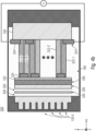
- Figs. 1a-b show a schematic representation of the optical resonator system 100 according to an embodiment.
- Fig. 1a shows a schematic plane view
- Fig. 1b shows a schematic cross-sectional view of the optical resonator system 100 according to the embodiment.
- STP slab tamm-plasmon-polariton
- the multi-strip waveguide structure 120 comprises a plurality of spaced semiconductor strips 122-1, ..., 122-n (122-#) for guiding an IR radiation R IR .
- the spaced semiconductor strips 122-1, ..., 122-n may be separated by means of dielectric strips 124 (e.g. air gaps or oxide).
- STP resonance structure 140 is exemplarily shown to comprise two semiconductor strips 142-1, 142-2, i.e. the number "m" of spaced semiconductor strips 142-1, ..., 142-m may be 2, for example.
- the numbers m, p usually do not vary due to physical reasons, wherein the widths of the strips 142-1, 142-2, 144-1, 144-2 are (exactly) defined individually, as will be explained below.
- the optical coupling structure 160 comprises a semiconductor layer 162, wherein the semiconductor layer 162 is arranged between the multi-strip waveguide structure 120 and the STP resonance structure 140 for optically coupling the IR radiation R IR between the multi-strip waveguide structure 120 and the STP resonance structure 140.
- the STP resonance structure 140 may be implemented as a Bragg mirror structure laterally extending in the system plane.
- the semiconductor material of the multi-strip waveguide structure 120, of the STP resonance structure 140 and of the coupling structure 160 may comprise a semiconductor material, e.g. a base layer 110 having a silicon or polysilicon material, which is applied on a first main surface region 180-A of a substrate or substrate structure 180 (see Fig. 1b ), which provides the system plane of the optical resonator system 100.
- the first dielectric layer 182 may comprise nitride material, e.g. SiN
- the semiconductor substrate layer 186 may comprise silicon.
- the substrate structure 180 comprises a cavity 188 vertically below the metal-semiconductor interface 146-A at the boundary region 140-1 of the STP resonance structure 140.
- the formation of the cavity 188 in the substrate structure 180 below the metal-semiconductor interface 146-A at the boundary region 140-1 of the STP resonance structure 140 reduces the heat transfer from the metal-semiconductor interface 146-A into the adjacent material.
- the first insulating layer 182 may comprise a thickness between 50 to 500 nm, between 100 and 200 nm, or of about 140 nm.
- the second insulating layer 114 may comprise a thickness between 500 to 5000 nm, between 1500 and 2500 nm, or of about 2000 nm.
- the semiconductor layer 186 may comprise a thickness between 50 to 500 nm, between 100 and 220 nm, or of about 160 nm.
- the principle of the optical resonator system 100 is based on exciting so-called Tamm plasmon polaritons, which may occur as optical resonances at the boundary (interface) 146-A between a Bragg mirror 140 and a metal 146.
- Bragg mirrors 142-# 142-1, ..., 142-m
- 144-# 144-1, ..., 144-p
- metal 146 i.e. the Tamm plasmon (TP) structure 140, are built with extended one-dimensional layers.
- the Bragg mirror 140 and the metal 146 are tuned and adjusted to each other, perpendicularly incident light of the resonant wavelength ⁇ RES (on the side of the Bragg mirror 140) will be fully absorbed by the resonance step-up (quality factor) of the field.
- the intrinsic losses of the metal are eventually responsible for complete absorption if the dielectrics are assumed to be approximately free from loss.
- This tuning (or matching) of the Bragg mirror 140 and the metal 146 refers to the individual amplitude reflection coefficients assigned to the Bragg mirror and the metal, respectively. Providing the employment of tungsten W, for example, this matching is considered in the design, as outlined below.
- the resonant absorption is also possible (e.g. with a different or lower performance), if other metals are used. Further, the design may be also tuned and optimized for other metals.
- the core of the present disclosure is the optical resonator system 100 whose starting point is the dielectric layer waveguide 120 made of polysilicon, for example.
- This resonator system 100 is depicted in Fig. 1a (upper area) and 1b (central area).
- the layers of the TP structures 140 are no longer be extended (approximately) infinitely in two dimensions (parallel to the x-y-plane) but are (vertically) restricted by the height h of the (polysilicon) layer (y direction, see Fig. 1b ).
- the metal layer 146 may comprise a stable, temperature-insensitive metal, such as W (tungsten), Ag (silver), Mo (Molybdenum), etc..
- the extension of the metal area/layer 146 may be selected, in principle, to be of any size. Only the relation to the membrane 180 surface must be taken into account for reasons concerning the heat flow.
- the width of the metal strip can be chosen arbitrarily wide, from an optical point-of-view. So it can be chosen to be convenient for fabrication and thermal aspects.
- the metal-semiconductor interface 146-A e.g. a tungsten/silicon interface
- That boundary layer (interface) 146-A is essential for the "slab Tamm plasmon polariton" (STP) structure (or layer Tamm plasmon structure) 140.
- STP label Tamm plasmon polariton
- the modeling is now faced with guided layer modes, where inclusion of the light is effected by the high refractive index of the silicon (e.g. poly-Si).
- STP resonance structures 140 as compared to one-dimensional TP structures is that, with/at optical resonance, there are radiation losses into space, and that resonance can be effected only for a specific polarization, namely when the electric field is parallel to the substrate surface, i.e. is transverse-electric polarized (TE-polarized) or s-polarized.
- the STP resonance structure 140 provide a (field) suppression remote from the resonant wavelength and from TE polarization, wherein the field's increase (step-up) in the plasmonic resonance results in an increase of emission/absorption at the resonance wavelength and TE polarization.
- the STP resonance structure 140 is a pure two-dimensional layer structure (infinite in its extension out of the plane).
- the STP structure 140 is coupled to the periodic strip waveguide (multi-strip waveguide, see lower area of Fig. 1a ) 120.
- the multi-strip waveguide 120 may be manufactured in an inexpensive manner by etching complete, continuous gaps of defined widths into a slab waveguide (planar waveguide) of polysilicon at periodic intervals or into the base layer 110, e.g. a silicon or poly-Si layer (at periodic intervals). Said type of waveguide 120 exhibits superior properties with regard to sensitivity (via simulation and experiment).
- the coupling of the multi-strip waveguide structure 120 to the STP resonance structure 140 is effected by means of the optical coupling structure 160, e.g. in form of a polysilicon layer (having an optimized lateral extension) between the STP structure 140 and the multi-strip waveguide 120.
- the optimized lateral extension may be derived from a semi-empirical optimization. It was found via simulation (by the inventors) that the optimized lateral extension may approximately corresponds to five times the averaged quarter-wavelength thickness considering the slab-waveguide and the coupled multi-strip-waveguide mode.
- the three-dimensional periodic unit cell is exemplarily shown in Figs. 1a-b .
- the resulting resonance wavelength range (target wavelength) ⁇ RES of the STP resonance structure 140 of the optical resonator structure 100 may be chosen in a range between 4.15 and 4.35 ⁇ m, for example.
- the semiconductor strips 122-# of the multi-strip waveguide structure 120 may have a width w between 1.3 and 1.5 ⁇ m, a height h between 0.9 and 1.1 ⁇ m and a distance (gap) g between 0.25 and 0.35 ⁇ m.
- the semiconductor strips 122-# of the multi-strip waveguide structure 120 may have a width w of 1.4 ⁇ m, a height h of 1 ⁇ m and a distance g of 0.3 ⁇ m.
- the further semiconductor strips 142-# ( 142-1 in Figs.
- the STP resonance structure 140 may have a width d 2 between 0.35 and 0.45 ⁇ m, a height h between 0.9 and 1.1 ⁇ m and a distance d 1 , d 3 (d 1 Air , d 3 Air ) between 0.5 and 0.6 ⁇ m.
- the semiconductor layer 162 of the coupling structure 160 may have a length d 0 between 1.7 and 2.1 ⁇ m and a height h between 0.9 and 1.1 ⁇ m. According to an embodiment, the semiconductor layer 162 of the coupling structure 160 may have a length d 0 of 1.9 ⁇ m and a height h of 1 ⁇ m.
- the multi-strip waveguide structure 120 comprises a plurality of slab waveguides 122-1, ..., 122-n for guiding slab modes of the IR radiation R IR .
- Fig. 2 shows a schematic top view of a narrowband mid-infrared radiation source 200 according to an embodiment.
- the narrowband mid-infrared radiation source 200 comprises the optical resonator system 100 as described above with respect to Figs. 1a-b , and an infrared radiation emitter 220 for emitting a broadband infrared radiation R IR to the STP resonance structure 140, wherein the IR radiation R IR in the resonance wavelength range ⁇ RES of the STP resonance structure 140 propagates from the STP resonance structure 140 to the optical coupling structure 160 and is coupled into the multi-strip waveguide structure 120.
- the STP resonance structure 140 is configured as an optical filter structure to filter the broadband infrared radiation R IR emitted by the infrared radiation emitter 220 and to provide the IR radiation R' IR as a filtered infrared radiation having a center wavelength ⁇ 0 according to the resonance wavelength range ⁇ RES of the STP resonance structure 140.
- the coupling structure 160 is configured to couple a mode of the IR radiation with the center wavelength ⁇ 0 into the multi-strip waveguide structure.
- the metal strip 146 adjacent to the semiconductor strip 142-2 at the boundary region 140-1 of the STP resonance structure 140 may be (optionally) arranged to form a heating element, i.e. the infrared radiation emitter 220.
- the metal (e. g. Ag, W, Mo, ...) 146 may be contacted so as to generate Joule heating by applying a voltage.
- a free standing (isolated) highly n-doped polysilicon wire 222 may be optionally provided as the heating element (thermal radiation emitter) 220, that emits broadband IR radiation R IR proportionally to the Planck's radiation law.
- the n-doped polysilicon wire may be heated in the vicinity of the Si/W boundary 146-1, as optionally depicted in Fig. 2 .
- the heating element 220 (optionally in form of the metal strip 146 or in form of doped polysilicon wire 222) may be configured to have in an actuated condition an operating temperature in a range between 600 and 1000 or between 600 and 700K.
- the metal strip 146 In the actuated condition of the metal strip 146, the metal strip 146 is connected to the voltage source V M .
- the polysilicon wire 222 In the actuated condition of the polysilicon wire 222, the polysilicon wire 222is connected to the voltage source V Si .
- the infrared radiation emitter is connected to a power source 240 for providing the electrical energy to bring the infrared radiation emitter in the actuated condition.
- Fig. 3 shows an exemplary schematic illustration of a fluid sensor 300 according to an embodiment.
- the mid-infrared radiation detector may comprise a thermopile structure, wherein the mid-infrared radiation detector is configured to sense an incoming guided infrared radiation which is a measure of the concentration of a target fluid F T in the surrounding atmosphere based on the evanescent field absorption effected by the target fluid F T .
- the interaction of the evanescent field component with the target fluid in the surrounding atmosphere results in a reduction of the transmitted IR radiation (guided infrared radiation transmitted by the multi-strip waveguide 120 between the emitter 200 and the detector 300) due to absorption which is a measure for the target fluid concentration in the surrounding atmosphere.
- the mid-infrared radiation detector may comprise at least one of a pyroelectric temperature sensor, a piezoelectric temperature sensor, a pn-junction temperature sensor and a resistive temperature sensor.
- the filtered IR radiation guided by the waveguide 120 comprises an evanescent field component for interacting with the surrounding atmosphere having the target fluid, wherein the interaction of the evanescent field component with the surrounding atmosphere results in a reduction of the transmitted thermal radiation R' IR due to absorption of the guided radiation R' IR which is a measure for the target fluid concentration in the surrounding atmosphere or medium.
- the fluid sensor 300 may provide a CMOS MID IR gas and liquid sensor for sensing the target fluid concentration (e.g. CO/ CO2/ O3/ NOx/ methane, for example) in the surrounding atmosphere or medium, based on a formation of a superimposed evanescent field, with narrowband mid-infrared radiation source 200 as described above with respect to Fig. 2 , and a mid-infrared radiation detector 320.
- the term fluid may relate to a liquid or a gas.
- the environmental medium relates to environmental air
- the target fluid may relate to a target gas or target gas component which is present in the environmental air.
- the present concept is equally applicable to sensing a target liquid or a target liquid component in the environmental medium.
- Fig. 4a shows a schematic cross-sectional view of a mid-infrared radiation detector 320 having a thermopile structure according to an embodiment.
- Fig. 4b shows a schematic cross-sectional view of the mid-infrared radiation detector 320 having a thermopile structure 320' according to the embodiment.
- the mid-infrared radiation detector 320 may be arranged on the substrate (or substrate structure) 180 having the plurality of layers 182, 184 and (optionally) 186.
- the substrate structure 180 comprises a further cavity 388 vertically below the thermopile structure.
- the formation of the cavity 388 in the substrate structure 180 reduces the heat transfer from the thermopile structure 320' into the adjacent material.
- the thermopile structure comprises a plurality of Si strips 322-1, 322-2 of alternating doping (phosphorus and boron) which are electrically connected by means of metal contacts 324 to provide a meander form of the connected metal strips 322-1, 322-2.
- the radiation detector 320 At the input portion of the thermopile structure 320' (adjacent to the waveguide 120), the radiation detector 320 comprises an alternating arrangement of semiconductor strips 326 and interjacent dielectric strips 328 (e.g. air gaps or oxide) and comprises a metal strip 330 adjacent to the semiconductor strip 326 at a boundary region 320-1 of the thermopile structure 320'.
- the alternating arrangement of semiconductor strips 326 and interjacent dielectric strips 328 is laterally sandwiched between the (semiconductor) region 120 and the metal 330.
- the mid-infrared radiation detector 320 forms a resonant absorber, which provides a wavelength-selective absorption and, subsequently, selective heat generation.
- the metal 330 is the absorptive element, the center of the heat-generation will be there. This results in a temperature difference between left and right side of the thermopile structure 320'.
- the purpose of the strip 332, e.g. a silica (SiO 2 ) strip is an electrical insulation from the metal contacts 324, while maintaining close thermal contact with the doped Si-strips 322-1, 322-2.
- the purpose of the semiconductor region 334 (Si-slab) is a thermal contact with the substrate 180.
- the metal 330 and the strip 332 next to the thermopile structure 320' should be as narrow as possible while the extent of the semiconductor region 334 may form an optimization parameter for the thermal design (depending on the membrane size, the thermal conductivity of the doped strips, etc) and may be equal to zero eventually.
- thermopile For measuring a selective detection and resonant absorption of the transmitted thermal radiation R' IR , an implementation by means of a thermopile is possible, as depicted in Figs. 4a-b .
- Selective absorption ensures selective heating in the area of the Si/metal boundary layer.
- a (detectable) voltage V is now generated by the Seebeck effect when the resonant wavelength is contacted by the STP resonance structure 140, i.e. transmitted from the STP resonance structure 140 over the multi-strip waveguide 120 to the mid-infrared radiation detector 220.
- a very high doped polysilicon e.g. a phosphorus doping concentration ( ⁇ 10 21 cm -3 ) close to the solubility limit).
- the substrate comprises a cavity vertically below at least one of the infrared radiation emitter and the mid-infrared radiation detector.
- the formation of the cavity 188, 388 in the substrate structure 180 below the thermal radiation emitter 120 and optionally below the thermal radiation detector 320 reduces the heat transfer from the thermal radiation emitter 120 and/or the thermal radiation detector 320 into the adjacent material so that the emission efficiency of the thermal radiation emitter as well as the detection efficiency of the thermal radiation detector can be increased.
- Fig. 6a-b show a selective absorption for different heights of the polysilicon layer for (a) air under the nitride membrane and (b) for oxide under the nitride membrane according to an embodiment.
- Fig. 7 shows (in form of a table) a summary of results for varying substrate materials (air/oxide) and SI layer thicknesses h ("inclusion factor evanescent field ⁇ , waveguide self-attenuation a, spectral emissivity at/with resonance ⁇ ( ⁇ r ), and Q factor of resonance").
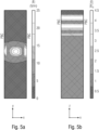
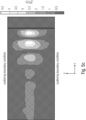
- Fig 5b-c just demonstrate the relative field enhancement from the simulation, which, in turn, is a measure for the possible improvement of the detection limit of such a resonant sensor in relation to a sensor featuring a broadband source.
- Figs 6 and 7 highlight the influence of the polysilicon thickness on the performance.
- the multi-strip waveguide structure comprises a plurality of spaced semiconductor strips for guiding an IR radiation.
- the STP resonance structure comprises an alternating arrangement of semiconductor strips and interjacent dielectric strips and comprises a metal strip adjacent to the semiconductor strip at a boundary region of the STP resonance structure.
- the metal strip and the adjacent semiconductor strip are arranged to provide a metal-semiconductor interface at the boundary region of the STP resonance structure, wherein the semiconductor strips of the multi-strip waveguide structure and the semiconductor strips of the STP resonance structure are arranged perpendicular to each other in a common system plane.
- the optical coupling structure having a semiconductor layer, wherein the semiconductor layer is arranged between the multi-strip waveguide structure and the STP resonance structure for optically coupling the IR radiation between the multi-strip waveguide structure and the STP resonance structure.
- the STP resonance structure is implemented as a Bragg mirror structure laterally extending in the system plane.
- the semiconductor material of the multi-strip waveguide structure, of the STP structure and of the coupling structure may comprise a semiconductor material, e.g. a silicon or polysilicon material, which is applied on a first main surface region of a substrate, which provides the system plane of the optical resonator system.
- a semiconductor material e.g. a silicon or polysilicon material
- the semiconductor strips of the multi-strip waveguide structure have a width between 1.3 and 1.5 ⁇ m, a height between 0.9 and 1.1 ⁇ m and a distance between 0.25 and 0.35 ⁇ m, and in particular a width of 1.4 ⁇ m, a height of 1 ⁇ m and a distance of 0.3 ⁇ m.
- the semiconductor strip at the boundary region of the STP resonance structure has a width between 1.0 and 1.15 ⁇ m and a height between 0.9 and 1.1 ⁇ m, and in particular a width of 1.07 ⁇ m and a height of 1 ⁇ m, wherein the further semiconductor strips of the STP resonance structure have a width between 0.35 and 0.45 ⁇ m, a height between 0.9 and 1.1 ⁇ m and a distance between 0.5 and 0.6 ⁇ m, and in particular a width of 0.4 ⁇ m, a height of 1 ⁇ m and a distance of 0.55 ⁇ m.
- the semiconductor layer of the coupling structure has a length between 1.7 and 2.1 ⁇ m and a height between 0.9 and 1.1 ⁇ m, and in particular a length of 1.9 ⁇ m and a height of 1 ⁇ m.
- the multi-strip waveguide structure comprises a plurality of slab waveguides for guiding slab modes of the IR radiation.
- a narrowband mid-infrared radiation source comprise the optical resonator system, and an infrared radiation emitter for emitting a broadband infrared radiation to the STP resonance structure, wherein the IR radiation in the resonance wavelength range of the STP resonance structure propagates from the STP resonance structure to the optical coupling structure and is coupled into the multi-strip waveguide structure.
- the STP structure is configured as an optical filter structure to filter the broadband infrared radiation emitted by the infrared radiation emitter and to provide the IR radiation as a filtered infrared radiation having a center wavelength according to the resonance wavelength range of the STP resonance structure.
- the multi-strip waveguide structure is configured to guide the (filtered) IR radiation having the center wavelength, wherein the guided IR radiation (the filtered IR radiation guided by the multi-strip waveguide structure) comprises an evanescent field component for interacting with the surrounding atmosphere.
- the coupling structure is configured to couple a mode of the IR radiation with the center wavelength ⁇ 0 into the multi-strip waveguide structure.
- the metal strip adjacent to the semiconductor strip at the boundary region of the STP resonance structure is arranged to form a heating element and is configured to have in an actuated condition an operating temperature in a range between 600 and 1000 or between 600 and 700K, and wherein the infrared radiation emitter is connected to a power source for providing the electrical energy to bring the infrared radiation emitter in the actuated condition.
- the mid-infrared radiation detector comprises a thermopile structure, wherein the mid-infrared radiation detector is configured to sense an incoming guided infrared radiation which is a measure of the concentration of a target fluid in the surrounding atmosphere based on the evanescent field absorption effected by the target fluid, wherein the interaction of the evanescent field component with the target fluid in the surrounding atmosphere results in a reduction of the transmitted IR radiation (guided infrared radiation transmitted by the multi-strip waveguide) due to absorption which is a measure for the target fluid concentration in the surrounding atmosphere.
- the transmitted IR radiation guided infrared radiation transmitted by the multi-strip waveguide
- the substrate comprises a cavity vertically below at least one of the infrared radiation emitter and the mid-infrared radiation detector.
- control circuitry can be implemented in hardware or in software or at least partially in hardware or at least partially in software.
- control circuitry can be implemented as a computer program product with a program code, the program code being operative for performing one of the methods when the computer program product runs on a computer.
- the program code may for example be stored on a machine readable carrier.
Landscapes
- Physics & Mathematics (AREA)
- General Physics & Mathematics (AREA)
- Health & Medical Sciences (AREA)
- Spectroscopy & Molecular Physics (AREA)
- Optics & Photonics (AREA)
- Chemical & Material Sciences (AREA)
- Life Sciences & Earth Sciences (AREA)
- Analytical Chemistry (AREA)
- Biochemistry (AREA)
- General Health & Medical Sciences (AREA)
- Immunology (AREA)
- Pathology (AREA)
- Microelectronics & Electronic Packaging (AREA)
- Engineering & Computer Science (AREA)
- Toxicology (AREA)
- Optical Integrated Circuits (AREA)
- Investigating Or Analysing Materials By Optical Means (AREA)
Priority Applications (3)
| Application Number | Priority Date | Filing Date | Title |
|---|---|---|---|
| EP21204001.8A EP4170321B1 (fr) | 2021-10-21 | 2021-10-21 | Système de résonateur optique, source de rayonnement infrarouge moyen à bande étroite et détecteur de fluide |
| US18/046,231 US12050340B2 (en) | 2021-10-21 | 2022-10-13 | Optical resonator system, narrowband mid-infrared radiation source |
| CN202211292650.9A CN116009146A (zh) | 2021-10-21 | 2022-10-20 | 光学谐振器系统、窄带中红外辐射源和流体传感器 |
Applications Claiming Priority (1)
| Application Number | Priority Date | Filing Date | Title |
|---|---|---|---|
| EP21204001.8A EP4170321B1 (fr) | 2021-10-21 | 2021-10-21 | Système de résonateur optique, source de rayonnement infrarouge moyen à bande étroite et détecteur de fluide |
Publications (2)
| Publication Number | Publication Date |
|---|---|
| EP4170321A1 true EP4170321A1 (fr) | 2023-04-26 |
| EP4170321B1 EP4170321B1 (fr) | 2025-01-29 |
Family
ID=78371853
Family Applications (1)
| Application Number | Title | Priority Date | Filing Date |
|---|---|---|---|
| EP21204001.8A Active EP4170321B1 (fr) | 2021-10-21 | 2021-10-21 | Système de résonateur optique, source de rayonnement infrarouge moyen à bande étroite et détecteur de fluide |
Country Status (3)
| Country | Link |
|---|---|
| US (1) | US12050340B2 (fr) |
| EP (1) | EP4170321B1 (fr) |
| CN (1) | CN116009146A (fr) |
Families Citing this family (1)
| Publication number | Priority date | Publication date | Assignee | Title |
|---|---|---|---|---|
| CN119556491B (zh) * | 2024-11-19 | 2025-09-16 | 华中科技大学 | 一种被动相干型长波红外辐射传感光子集成器件 |
Citations (1)
| Publication number | Priority date | Publication date | Assignee | Title |
|---|---|---|---|---|
| US20200309686A1 (en) * | 2019-03-27 | 2020-10-01 | Infineon Technologies Ag | Fluid sensor and method for manufacturing a fluid sensor |
Family Cites Families (4)
| Publication number | Priority date | Publication date | Assignee | Title |
|---|---|---|---|---|
| FR2965665B1 (fr) * | 2010-09-30 | 2012-10-26 | Centre Nat Rech Scient | Sources et capteurs de lumière comprenant au moins une microcavite a mode de tamm plasmonique localise |
| WO2019225726A1 (fr) * | 2018-05-25 | 2019-11-28 | 国立研究開発法人物質・材料研究機構 | Sources de lumière à rayonnement stratifié |
| EP3705872B1 (fr) * | 2019-03-08 | 2025-07-09 | Infineon Technologies AG | Capteur de gaz |
| US11929703B2 (en) * | 2021-03-10 | 2024-03-12 | Atomos Nuclear and Space Corporation | System and method for converting and transmitting energy |
-
2021
- 2021-10-21 EP EP21204001.8A patent/EP4170321B1/fr active Active
-
2022
- 2022-10-13 US US18/046,231 patent/US12050340B2/en active Active
- 2022-10-20 CN CN202211292650.9A patent/CN116009146A/zh active Pending
Patent Citations (1)
| Publication number | Priority date | Publication date | Assignee | Title |
|---|---|---|---|---|
| US20200309686A1 (en) * | 2019-03-27 | 2020-10-01 | Infineon Technologies Ag | Fluid sensor and method for manufacturing a fluid sensor |
Non-Patent Citations (3)
| Title |
|---|
| PÜHRINGER GERALD ET AL: "Highly Selective CMOS-Compatible Mid-Infrared Thermal Emitter/Detector Slab Design Using Optical Tamm-States", MATERIALS, vol. 12, no. 6, 20 March 2019 (2019-03-20), pages 929, XP055894179, DOI: 10.3390/ma12060929 * |
| PUHRINGER GERALD ET AL: "Modeling of a CMOS-Compatible Slab Tamm Plasmon Absorber using N-Type Silicon", 2019 IEEE SENSORS, IEEE, 27 October 2019 (2019-10-27), pages 1 - 4, XP033685754, DOI: 10.1109/SENSORS43011.2019.8956847 * |
| VENTSISLAV LAVCHIEV ET AL: "Mid-infrared rib waveguide absorption sensors based on Si", PROCEEDINGS OF SPIE, vol. 8763, 17 May 2013 (2013-05-17), pages 87632F, XP055100990, ISSN: 0277-786X, DOI: 10.1117/12.2017273 * |
Also Published As
| Publication number | Publication date |
|---|---|
| EP4170321B1 (fr) | 2025-01-29 |
| CN116009146A (zh) | 2023-04-25 |
| US20230125167A1 (en) | 2023-04-27 |
| US12050340B2 (en) | 2024-07-30 |
Similar Documents
| Publication | Publication Date | Title |
|---|---|---|
| US10598590B2 (en) | Sensor device and a method of detecting a component in gas | |
| US11506599B2 (en) | Fluid sensor including an optical filter and a waveguide, and method for manufacturing the fluid sensor | |
| US9372114B2 (en) | Spectrophotometer comprising an integrated Fabry-Perot interferometer | |
| US20180374981A1 (en) | Metamaterial Thermal Pixel for Limited Bandwidth Electromagnetic Sourcing and Detection | |
| CN111665211B (zh) | 气体传感器 | |
| Siebert et al. | Infrared integrated optical evanescent field sensor for gas analysis: Part I: System design | |
| CN103733354B (zh) | 太赫兹探测单元 | |
| Negm et al. | Graphene thermal infrared emitters integrated into silicon photonic waveguides | |
| US12050340B2 (en) | Optical resonator system, narrowband mid-infrared radiation source | |
| TWI512963B (zh) | 光偵測器 | |
| WO2020086004A1 (fr) | Thermocouple, thermopile et dispositifs | |
| JP6269008B2 (ja) | 電磁波−表面ポラリトン変換素子。 | |
| CN107907237B (zh) | 一种光学吸收型温度传感器 | |
| CN114324225A (zh) | 一种应用于气体传感的可调控光谱响应的微纳米装置 | |
| Liao et al. | Multi-band microbolometer in CMOS technology | |
| US20260126677A1 (en) | Optical sources including heating elements and optical waveguides and related photonic integrated circuit devices | |
| US11073474B2 (en) | Device and method for detecting the presence of determined molecules, and biosensor | |
| Zhao et al. | Infrared detection using plasmonically enhanced thermomechanically actuated nanowire arrays | |
| JP2024130550A (ja) | 光半導体デバイス | |
| Zhao et al. | Plasmo-thermomechanical suspended nanowire array detectors for mid-infrared spectrum |
Legal Events
| Date | Code | Title | Description |
|---|---|---|---|
| PUAI | Public reference made under article 153(3) epc to a published international application that has entered the european phase |
Free format text: ORIGINAL CODE: 0009012 |
|
| STAA | Information on the status of an ep patent application or granted ep patent |
Free format text: STATUS: THE APPLICATION HAS BEEN PUBLISHED |
|
| AK | Designated contracting states |
Kind code of ref document: A1 Designated state(s): AL AT BE BG CH CY CZ DE DK EE ES FI FR GB GR HR HU IE IS IT LI LT LU LV MC MK MT NL NO PL PT RO RS SE SI SK SM TR |
|
| STAA | Information on the status of an ep patent application or granted ep patent |
Free format text: STATUS: REQUEST FOR EXAMINATION WAS MADE |
|
| 17P | Request for examination filed |
Effective date: 20230505 |
|
| RBV | Designated contracting states (corrected) |
Designated state(s): AL AT BE BG CH CY CZ DE DK EE ES FI FR GB GR HR HU IE IS IT LI LT LU LV MC MK MT NL NO PL PT RO RS SE SI SK SM TR |
|
| GRAP | Despatch of communication of intention to grant a patent |
Free format text: ORIGINAL CODE: EPIDOSNIGR1 |
|
| STAA | Information on the status of an ep patent application or granted ep patent |
Free format text: STATUS: GRANT OF PATENT IS INTENDED |
|
| INTG | Intention to grant announced |
Effective date: 20240902 |
|
| RIN1 | Information on inventor provided before grant (corrected) |
Inventor name: TORTSCHANOFF, ANDREAS Inventor name: FLEURY, CLEMENT Inventor name: CONSANI, CRISTINA Inventor name: STOCKER, GERALD Inventor name: GRILLE, THOMAS Inventor name: JANNESARI, REYHANEH Inventor name: JAKOBY, BERNHARD Inventor name: PUEHRINGER, GERALD |
|
| P01 | Opt-out of the competence of the unified patent court (upc) registered |
Free format text: CASE NUMBER: APP_54674/2024 Effective date: 20241004 |
|
| GRAS | Grant fee paid |
Free format text: ORIGINAL CODE: EPIDOSNIGR3 |
|
| GRAA | (expected) grant |
Free format text: ORIGINAL CODE: 0009210 |
|
| STAA | Information on the status of an ep patent application or granted ep patent |
Free format text: STATUS: THE PATENT HAS BEEN GRANTED |
|
| AK | Designated contracting states |
Kind code of ref document: B1 Designated state(s): AL AT BE BG CH CY CZ DE DK EE ES FI FR GB GR HR HU IE IS IT LI LT LU LV MC MK MT NL NO PL PT RO RS SE SI SK SM TR |
|
| REG | Reference to a national code |
Ref country code: GB Ref legal event code: FG4D |
|
| REG | Reference to a national code |
Ref country code: CH Ref legal event code: EP |
|
| REG | Reference to a national code |
Ref country code: DE Ref legal event code: R096 Ref document number: 602021025328 Country of ref document: DE |
|
| REG | Reference to a national code |
Ref country code: IE Ref legal event code: FG4D |
|
| REG | Reference to a national code |
Ref country code: NL Ref legal event code: MP Effective date: 20250129 |
|
| PG25 | Lapsed in a contracting state [announced via postgrant information from national office to epo] |
Ref country code: NL Free format text: LAPSE BECAUSE OF FAILURE TO SUBMIT A TRANSLATION OF THE DESCRIPTION OR TO PAY THE FEE WITHIN THE PRESCRIBED TIME-LIMIT Effective date: 20250129 |
|
| PG25 | Lapsed in a contracting state [announced via postgrant information from national office to epo] |
Ref country code: RS Free format text: LAPSE BECAUSE OF FAILURE TO SUBMIT A TRANSLATION OF THE DESCRIPTION OR TO PAY THE FEE WITHIN THE PRESCRIBED TIME-LIMIT Effective date: 20250429 |
|
| PG25 | Lapsed in a contracting state [announced via postgrant information from national office to epo] |
Ref country code: FI Free format text: LAPSE BECAUSE OF FAILURE TO SUBMIT A TRANSLATION OF THE DESCRIPTION OR TO PAY THE FEE WITHIN THE PRESCRIBED TIME-LIMIT Effective date: 20250129 |
|
| PG25 | Lapsed in a contracting state [announced via postgrant information from national office to epo] |
Ref country code: PL Free format text: LAPSE BECAUSE OF FAILURE TO SUBMIT A TRANSLATION OF THE DESCRIPTION OR TO PAY THE FEE WITHIN THE PRESCRIBED TIME-LIMIT Effective date: 20250129 |
|
| PG25 | Lapsed in a contracting state [announced via postgrant information from national office to epo] |
Ref country code: ES Free format text: LAPSE BECAUSE OF FAILURE TO SUBMIT A TRANSLATION OF THE DESCRIPTION OR TO PAY THE FEE WITHIN THE PRESCRIBED TIME-LIMIT Effective date: 20250129 |
|
| REG | Reference to a national code |
Ref country code: LT Ref legal event code: MG9D |
|
| PG25 | Lapsed in a contracting state [announced via postgrant information from national office to epo] |
Ref country code: IS Free format text: LAPSE BECAUSE OF FAILURE TO SUBMIT A TRANSLATION OF THE DESCRIPTION OR TO PAY THE FEE WITHIN THE PRESCRIBED TIME-LIMIT Effective date: 20250529 Ref country code: NO Free format text: LAPSE BECAUSE OF FAILURE TO SUBMIT A TRANSLATION OF THE DESCRIPTION OR TO PAY THE FEE WITHIN THE PRESCRIBED TIME-LIMIT Effective date: 20250429 |
|
| REG | Reference to a national code |
Ref country code: AT Ref legal event code: MK05 Ref document number: 1763908 Country of ref document: AT Kind code of ref document: T Effective date: 20250129 |
|
| PG25 | Lapsed in a contracting state [announced via postgrant information from national office to epo] |
Ref country code: HR Free format text: LAPSE BECAUSE OF FAILURE TO SUBMIT A TRANSLATION OF THE DESCRIPTION OR TO PAY THE FEE WITHIN THE PRESCRIBED TIME-LIMIT Effective date: 20250129 |
|
| PG25 | Lapsed in a contracting state [announced via postgrant information from national office to epo] |
Ref country code: LV Free format text: LAPSE BECAUSE OF FAILURE TO SUBMIT A TRANSLATION OF THE DESCRIPTION OR TO PAY THE FEE WITHIN THE PRESCRIBED TIME-LIMIT Effective date: 20250129 Ref country code: PT Free format text: LAPSE BECAUSE OF FAILURE TO SUBMIT A TRANSLATION OF THE DESCRIPTION OR TO PAY THE FEE WITHIN THE PRESCRIBED TIME-LIMIT Effective date: 20250529 |
|
| PG25 | Lapsed in a contracting state [announced via postgrant information from national office to epo] |
Ref country code: BG Free format text: LAPSE BECAUSE OF FAILURE TO SUBMIT A TRANSLATION OF THE DESCRIPTION OR TO PAY THE FEE WITHIN THE PRESCRIBED TIME-LIMIT Effective date: 20250129 Ref country code: GR Free format text: LAPSE BECAUSE OF FAILURE TO SUBMIT A TRANSLATION OF THE DESCRIPTION OR TO PAY THE FEE WITHIN THE PRESCRIBED TIME-LIMIT Effective date: 20250430 |
|
| PG25 | Lapsed in a contracting state [announced via postgrant information from national office to epo] |
Ref country code: AT Free format text: LAPSE BECAUSE OF FAILURE TO SUBMIT A TRANSLATION OF THE DESCRIPTION OR TO PAY THE FEE WITHIN THE PRESCRIBED TIME-LIMIT Effective date: 20250129 |
|
| PG25 | Lapsed in a contracting state [announced via postgrant information from national office to epo] |
Ref country code: SE Free format text: LAPSE BECAUSE OF FAILURE TO SUBMIT A TRANSLATION OF THE DESCRIPTION OR TO PAY THE FEE WITHIN THE PRESCRIBED TIME-LIMIT Effective date: 20250129 |
|
| PG25 | Lapsed in a contracting state [announced via postgrant information from national office to epo] |
Ref country code: SM Free format text: LAPSE BECAUSE OF FAILURE TO SUBMIT A TRANSLATION OF THE DESCRIPTION OR TO PAY THE FEE WITHIN THE PRESCRIBED TIME-LIMIT Effective date: 20250129 |
|
| PG25 | Lapsed in a contracting state [announced via postgrant information from national office to epo] |
Ref country code: DK Free format text: LAPSE BECAUSE OF FAILURE TO SUBMIT A TRANSLATION OF THE DESCRIPTION OR TO PAY THE FEE WITHIN THE PRESCRIBED TIME-LIMIT Effective date: 20250129 |
|
| PG25 | Lapsed in a contracting state [announced via postgrant information from national office to epo] |
Ref country code: IT Free format text: LAPSE BECAUSE OF FAILURE TO SUBMIT A TRANSLATION OF THE DESCRIPTION OR TO PAY THE FEE WITHIN THE PRESCRIBED TIME-LIMIT Effective date: 20250129 |
|
| PG25 | Lapsed in a contracting state [announced via postgrant information from national office to epo] |
Ref country code: EE Free format text: LAPSE BECAUSE OF FAILURE TO SUBMIT A TRANSLATION OF THE DESCRIPTION OR TO PAY THE FEE WITHIN THE PRESCRIBED TIME-LIMIT Effective date: 20250129 Ref country code: CZ Free format text: LAPSE BECAUSE OF FAILURE TO SUBMIT A TRANSLATION OF THE DESCRIPTION OR TO PAY THE FEE WITHIN THE PRESCRIBED TIME-LIMIT Effective date: 20250129 |
|
| PG25 | Lapsed in a contracting state [announced via postgrant information from national office to epo] |
Ref country code: RO Free format text: LAPSE BECAUSE OF FAILURE TO SUBMIT A TRANSLATION OF THE DESCRIPTION OR TO PAY THE FEE WITHIN THE PRESCRIBED TIME-LIMIT Effective date: 20250129 |
|
| PG25 | Lapsed in a contracting state [announced via postgrant information from national office to epo] |
Ref country code: SK Free format text: LAPSE BECAUSE OF FAILURE TO SUBMIT A TRANSLATION OF THE DESCRIPTION OR TO PAY THE FEE WITHIN THE PRESCRIBED TIME-LIMIT Effective date: 20250129 |
|
| REG | Reference to a national code |
Ref country code: DE Ref legal event code: R097 Ref document number: 602021025328 Country of ref document: DE |
|
| PLBE | No opposition filed within time limit |
Free format text: ORIGINAL CODE: 0009261 |
|
| STAA | Information on the status of an ep patent application or granted ep patent |
Free format text: STATUS: NO OPPOSITION FILED WITHIN TIME LIMIT |
|
| 26N | No opposition filed |
Effective date: 20251030 |
|
| PGFP | Annual fee paid to national office [announced via postgrant information from national office to epo] |
Ref country code: DE Payment date: 20251217 Year of fee payment: 5 |