EP4170416A1 - Écran d'affichage et dispositif d'affichage - Google Patents
Écran d'affichage et dispositif d'affichage Download PDFInfo
- Publication number
- EP4170416A1 EP4170416A1 EP20870442.9A EP20870442A EP4170416A1 EP 4170416 A1 EP4170416 A1 EP 4170416A1 EP 20870442 A EP20870442 A EP 20870442A EP 4170416 A1 EP4170416 A1 EP 4170416A1
- Authority
- EP
- European Patent Office
- Prior art keywords
- substrate
- electrode
- micro led
- lighting unit
- led lighting
- Prior art date
- Legal status (The legal status is an assumption and is not a legal conclusion. Google has not performed a legal analysis and makes no representation as to the accuracy of the status listed.)
- Pending
Links
Images



Classifications
-
- G—PHYSICS
- G02—OPTICS
- G02F—OPTICAL DEVICES OR ARRANGEMENTS FOR THE CONTROL OF LIGHT BY MODIFICATION OF THE OPTICAL PROPERTIES OF THE MEDIA OF THE ELEMENTS INVOLVED THEREIN; NON-LINEAR OPTICS; FREQUENCY-CHANGING OF LIGHT; OPTICAL LOGIC ELEMENTS; OPTICAL ANALOGUE/DIGITAL CONVERTERS
- G02F1/00—Devices or arrangements for the control of the intensity, colour, phase, polarisation or direction of light arriving from an independent light source, e.g. switching, gating or modulating; Non-linear optics
- G02F1/01—Devices or arrangements for the control of the intensity, colour, phase, polarisation or direction of light arriving from an independent light source, e.g. switching, gating or modulating; Non-linear optics for the control of the intensity, phase, polarisation or colour
- G02F1/13—Devices or arrangements for the control of the intensity, colour, phase, polarisation or direction of light arriving from an independent light source, e.g. switching, gating or modulating; Non-linear optics for the control of the intensity, phase, polarisation or colour based on liquid crystals, e.g. single liquid crystal display cells
- G02F1/133—Constructional arrangements; Operation of liquid crystal cells; Circuit arrangements
- G02F1/1333—Constructional arrangements; Manufacturing methods
-
- G—PHYSICS
- G02—OPTICS
- G02F—OPTICAL DEVICES OR ARRANGEMENTS FOR THE CONTROL OF LIGHT BY MODIFICATION OF THE OPTICAL PROPERTIES OF THE MEDIA OF THE ELEMENTS INVOLVED THEREIN; NON-LINEAR OPTICS; FREQUENCY-CHANGING OF LIGHT; OPTICAL LOGIC ELEMENTS; OPTICAL ANALOGUE/DIGITAL CONVERTERS
- G02F1/00—Devices or arrangements for the control of the intensity, colour, phase, polarisation or direction of light arriving from an independent light source, e.g. switching, gating or modulating; Non-linear optics
- G02F1/01—Devices or arrangements for the control of the intensity, colour, phase, polarisation or direction of light arriving from an independent light source, e.g. switching, gating or modulating; Non-linear optics for the control of the intensity, phase, polarisation or colour
- G02F1/13—Devices or arrangements for the control of the intensity, colour, phase, polarisation or direction of light arriving from an independent light source, e.g. switching, gating or modulating; Non-linear optics for the control of the intensity, phase, polarisation or colour based on liquid crystals, e.g. single liquid crystal display cells
- G02F1/133—Constructional arrangements; Operation of liquid crystal cells; Circuit arrangements
- G02F1/1333—Constructional arrangements; Manufacturing methods
- G02F1/1335—Structural association of cells with optical devices, e.g. polarisers or reflectors
- G02F1/133509—Filters, e.g. light shielding masks
- G02F1/133514—Colour filters
-
- G—PHYSICS
- G02—OPTICS
- G02F—OPTICAL DEVICES OR ARRANGEMENTS FOR THE CONTROL OF LIGHT BY MODIFICATION OF THE OPTICAL PROPERTIES OF THE MEDIA OF THE ELEMENTS INVOLVED THEREIN; NON-LINEAR OPTICS; FREQUENCY-CHANGING OF LIGHT; OPTICAL LOGIC ELEMENTS; OPTICAL ANALOGUE/DIGITAL CONVERTERS
- G02F1/00—Devices or arrangements for the control of the intensity, colour, phase, polarisation or direction of light arriving from an independent light source, e.g. switching, gating or modulating; Non-linear optics
- G02F1/01—Devices or arrangements for the control of the intensity, colour, phase, polarisation or direction of light arriving from an independent light source, e.g. switching, gating or modulating; Non-linear optics for the control of the intensity, phase, polarisation or colour
- G02F1/13—Devices or arrangements for the control of the intensity, colour, phase, polarisation or direction of light arriving from an independent light source, e.g. switching, gating or modulating; Non-linear optics for the control of the intensity, phase, polarisation or colour based on liquid crystals, e.g. single liquid crystal display cells
- G02F1/133—Constructional arrangements; Operation of liquid crystal cells; Circuit arrangements
- G02F1/1333—Constructional arrangements; Manufacturing methods
- G02F1/1335—Structural association of cells with optical devices, e.g. polarisers or reflectors
- G02F1/1336—Illuminating devices
-
- G—PHYSICS
- G02—OPTICS
- G02F—OPTICAL DEVICES OR ARRANGEMENTS FOR THE CONTROL OF LIGHT BY MODIFICATION OF THE OPTICAL PROPERTIES OF THE MEDIA OF THE ELEMENTS INVOLVED THEREIN; NON-LINEAR OPTICS; FREQUENCY-CHANGING OF LIGHT; OPTICAL LOGIC ELEMENTS; OPTICAL ANALOGUE/DIGITAL CONVERTERS
- G02F1/00—Devices or arrangements for the control of the intensity, colour, phase, polarisation or direction of light arriving from an independent light source, e.g. switching, gating or modulating; Non-linear optics
- G02F1/01—Devices or arrangements for the control of the intensity, colour, phase, polarisation or direction of light arriving from an independent light source, e.g. switching, gating or modulating; Non-linear optics for the control of the intensity, phase, polarisation or colour
- G02F1/13—Devices or arrangements for the control of the intensity, colour, phase, polarisation or direction of light arriving from an independent light source, e.g. switching, gating or modulating; Non-linear optics for the control of the intensity, phase, polarisation or colour based on liquid crystals, e.g. single liquid crystal display cells
- G02F1/133—Constructional arrangements; Operation of liquid crystal cells; Circuit arrangements
- G02F1/1333—Constructional arrangements; Manufacturing methods
- G02F1/1335—Structural association of cells with optical devices, e.g. polarisers or reflectors
- G02F1/1336—Illuminating devices
- G02F1/133602—Direct backlight
- G02F1/133603—Direct backlight with LEDs
-
- G—PHYSICS
- G02—OPTICS
- G02F—OPTICAL DEVICES OR ARRANGEMENTS FOR THE CONTROL OF LIGHT BY MODIFICATION OF THE OPTICAL PROPERTIES OF THE MEDIA OF THE ELEMENTS INVOLVED THEREIN; NON-LINEAR OPTICS; FREQUENCY-CHANGING OF LIGHT; OPTICAL LOGIC ELEMENTS; OPTICAL ANALOGUE/DIGITAL CONVERTERS
- G02F1/00—Devices or arrangements for the control of the intensity, colour, phase, polarisation or direction of light arriving from an independent light source, e.g. switching, gating or modulating; Non-linear optics
- G02F1/01—Devices or arrangements for the control of the intensity, colour, phase, polarisation or direction of light arriving from an independent light source, e.g. switching, gating or modulating; Non-linear optics for the control of the intensity, phase, polarisation or colour
- G02F1/13—Devices or arrangements for the control of the intensity, colour, phase, polarisation or direction of light arriving from an independent light source, e.g. switching, gating or modulating; Non-linear optics for the control of the intensity, phase, polarisation or colour based on liquid crystals, e.g. single liquid crystal display cells
- G02F1/133—Constructional arrangements; Operation of liquid crystal cells; Circuit arrangements
- G02F1/136—Liquid crystal cells structurally associated with a semi-conducting layer or substrate, e.g. cells forming part of an integrated circuit
- G02F1/1362—Active matrix addressed cells
- G02F1/136222—Colour filters incorporated in the active matrix substrate
-
- G—PHYSICS
- G02—OPTICS
- G02F—OPTICAL DEVICES OR ARRANGEMENTS FOR THE CONTROL OF LIGHT BY MODIFICATION OF THE OPTICAL PROPERTIES OF THE MEDIA OF THE ELEMENTS INVOLVED THEREIN; NON-LINEAR OPTICS; FREQUENCY-CHANGING OF LIGHT; OPTICAL LOGIC ELEMENTS; OPTICAL ANALOGUE/DIGITAL CONVERTERS
- G02F1/00—Devices or arrangements for the control of the intensity, colour, phase, polarisation or direction of light arriving from an independent light source, e.g. switching, gating or modulating; Non-linear optics
- G02F1/01—Devices or arrangements for the control of the intensity, colour, phase, polarisation or direction of light arriving from an independent light source, e.g. switching, gating or modulating; Non-linear optics for the control of the intensity, phase, polarisation or colour
- G02F1/13—Devices or arrangements for the control of the intensity, colour, phase, polarisation or direction of light arriving from an independent light source, e.g. switching, gating or modulating; Non-linear optics for the control of the intensity, phase, polarisation or colour based on liquid crystals, e.g. single liquid crystal display cells
- G02F1/133—Constructional arrangements; Operation of liquid crystal cells; Circuit arrangements
- G02F1/136—Liquid crystal cells structurally associated with a semi-conducting layer or substrate, e.g. cells forming part of an integrated circuit
- G02F1/1362—Active matrix addressed cells
- G02F1/136286—Wiring, e.g. gate line, drain line
-
- G—PHYSICS
- G09—EDUCATION; CRYPTOGRAPHY; DISPLAY; ADVERTISING; SEALS
- G09F—DISPLAYING; ADVERTISING; SIGNS; LABELS OR NAME-PLATES; SEALS
- G09F9/00—Indicating arrangements for variable information in which the information is built-up on a support by selection or combination of individual elements
- G09F9/30—Indicating arrangements for variable information in which the information is built-up on a support by selection or combination of individual elements in which the desired character or characters are formed by combining individual elements
- G09F9/33—Indicating arrangements for variable information in which the information is built-up on a support by selection or combination of individual elements in which the desired character or characters are formed by combining individual elements being semiconductor devices, e.g. diodes
-
- G—PHYSICS
- G02—OPTICS
- G02F—OPTICAL DEVICES OR ARRANGEMENTS FOR THE CONTROL OF LIGHT BY MODIFICATION OF THE OPTICAL PROPERTIES OF THE MEDIA OF THE ELEMENTS INVOLVED THEREIN; NON-LINEAR OPTICS; FREQUENCY-CHANGING OF LIGHT; OPTICAL LOGIC ELEMENTS; OPTICAL ANALOGUE/DIGITAL CONVERTERS
- G02F1/00—Devices or arrangements for the control of the intensity, colour, phase, polarisation or direction of light arriving from an independent light source, e.g. switching, gating or modulating; Non-linear optics
- G02F1/01—Devices or arrangements for the control of the intensity, colour, phase, polarisation or direction of light arriving from an independent light source, e.g. switching, gating or modulating; Non-linear optics for the control of the intensity, phase, polarisation or colour
- G02F1/13—Devices or arrangements for the control of the intensity, colour, phase, polarisation or direction of light arriving from an independent light source, e.g. switching, gating or modulating; Non-linear optics for the control of the intensity, phase, polarisation or colour based on liquid crystals, e.g. single liquid crystal display cells
- G02F1/133—Constructional arrangements; Operation of liquid crystal cells; Circuit arrangements
- G02F1/136—Liquid crystal cells structurally associated with a semi-conducting layer or substrate, e.g. cells forming part of an integrated circuit
- G02F1/1362—Active matrix addressed cells
- G02F1/1368—Active matrix addressed cells in which the switching element is a three-electrode device
- G02F1/13685—Top gates
-
- G—PHYSICS
- G02—OPTICS
- G02F—OPTICAL DEVICES OR ARRANGEMENTS FOR THE CONTROL OF LIGHT BY MODIFICATION OF THE OPTICAL PROPERTIES OF THE MEDIA OF THE ELEMENTS INVOLVED THEREIN; NON-LINEAR OPTICS; FREQUENCY-CHANGING OF LIGHT; OPTICAL LOGIC ELEMENTS; OPTICAL ANALOGUE/DIGITAL CONVERTERS
- G02F2201/00—Constructional arrangements not provided for in groups G02F1/00 - G02F7/00
- G02F2201/44—Arrangements combining different electro-active layers, e.g. electrochromic, liquid crystal or electroluminescent layers
Definitions
- the present invention relates to a display technique, and more particularly, to a display panel and a display device.
- Under-screen sensing technique becomes a development key point in a medium/small-size display device due to the demands for full-screen and integrated display device. Because the LCD panel is a passive lighting device illuminated by the backlight module, the optical sensor and the optical display cannot be spatially overlapped. Therefore, it becomes more difficult for LCD panel to become a full-screen device.
- OLED panel In contrast to LCD panel, OLED panel is an active lighting device illuminated by each OLED pixel. OLED panel has advantages such as high contrast, thin, flexible and bendable. In addition, because the OLED panel does not need a backlight module, it can be well integrated with the conventional optical sensor. Thus, the integrated optical sensing technique has become a unique advantage of the OLED panel and allows the OLED panel to be switched between the display mode and the imaging mode. Furthermore, LCD panel has a carved out area but the carved out area cannot be used to display images but OLED panel does not have this issue.
- the LCD panel has a low-cost advantage, this advantage becomes unimportant because of the increasing demands of the full-screen. Therefore, it is important to improve the conventional LCD panel to meet the full-screen demands.
- One objective of an embodiment of the present invention is to provide a display panel and a display device to solve the above-mentioned issue where a conventional LCD panel cannot spatially overlap the optical sensor and the display in order to further meet the full-screen demand.
- a display panel is disclosed.
- the display panel comprises a first pixel area and a second pixel area adjacent to the first pixel area.
- the display panel comprises an array substrate, a color film substrate arranged oppositely to the array substrate, a liquid crystal layer between the array substrate and the color film substrate, and a backlight module positioned at a side of the color film substrate, which is back on to the array substrate.
- the display panel comprises a plurality of micro light emitting diode (micro LED) lighting unit, a transparent area is placed among the micro LED lighting unit, and the color film substrate comprises a color filter in the second pixel area.
- micro LED micro light emitting diode
- the micro LED lighting unit comprises a electrode surface and a substrate surface opposite to the electrode surface, the electrode surface has a first electrode, the micro LED lighting unit is placed to have the electrode surface face the backlight module, and a lighting direction of the micro LED lighting unit is from the electrode surface to the substrate surface.
- the color film substrate comprises:
- the color filter is positioned correspondingly to the second pixel area on the first substrate.
- a second electrode corresponding to the first electrode is placed in the first pixel area of the first substrate.
- the micro LED lighting unit and the color filter are located on a side of the first substrate, which is back on to the backlight module, and the first electrode of the micro LED lighting unit is electrically connected to the second electrode.
- the micro LED lighting unit is placed on a side of the first substrate, which is close to the backlight module, the color filter is placed on a side of the first substrate, which is back on to the backlight module, and the micro LED lighting unit is electrically connected to the second electrode through the first electrode.
- the first electrode extends from the electrode surface to a position corresponding to the second electrode along a side surface of the micro LED lighting unit.
- the color film substrate further comprises a first driving circuit, the first driving circuit is corresponding to the first pixel area and placed on a side surface of the first substrate, which is facing the micro LED lighting unit, the micro LED lighting unit is electrically connected to the first driving circuit.
- the first driving circuit comprises scan lines extending horizontally and data lines extending vertically, two adjacent scan lines and two adjacent scan lines define a sub-pixel area, and an orthogonal projection of the Micro Led lighting unit on the first substrate is smaller than an area of the sub-pixel area.
- the orthogonal projection of the micro LED lighting unit on the first substrate occupies 10%-50% of an area of the sub-pixel area, and the micro LED lighting unit comprises a red lighting unit, a green lighting unit and a blue lighting unit.
- the array substrate comprises:
- a second electrode corresponding to the first electrode is placed on a position the second substrate, which corresponds to the first pixel area; and the first electrode is electrically connected to the second electrode.
- the first electrode extends from an electrode surface of the micro LED lighting unit to a position of the second substrate, which is corresponding to the second electrode, along a side surface of the micro LED lighting unit.
- the array substrate further comprises a second driving circuit, corresponding to the second pixel area and placed on the second substrate.
- a display device includes a display panel.
- the display panel includes a first pixel area and a second pixel area adjacent to the first pixel area.
- the display panel comprises an array substrate, a color film substrate arranged oppositely to the array substrate, a liquid crystal layer between the array substrate and the color film substrate, and a backlight module positioned at a side of the color film substrate, which is back on to the array substrate.
- the display panel comprises a plurality of micro light emitting diode (micro LED) lighting units, a transparent area is placed among the micro LED lighting units, and the color film substrate comprises a color filter in the second pixel area.
- micro LED micro light emitting diode
- the micro LED lighting unit comprises a electrode surface and a substrate surface opposite to the electrode surface, the electrode surface has a first electrode, the micro LED lighting unit is placed to have the electrode surface face the backlight module, and a lighting direction of the micro LED lighting unit is from the electrode surface to the substrate surface.
- the color film substrate comprises:
- the color filter is positioned correspondingly to the second pixel area on the first substrate.
- a second electrode corresponding to the first electrode is placed in the first pixel area of the first substrate.
- the microLED lighting unit and the color filter are located on a side of the first substrate, which is back on to the backlight module, and the first electrode of the micro LED lighting unit is electrically connected to the second electrode.
- the micro LED lighting unit is placed on a side of the first substrate, which is close to the backlight module, the color filter is placed on a side of the first substrate, which is back on to the backlight module, and the micro LED lighting unit is electrically connected to the second electrode through the first electrode.
- the first electrode extends from the electrode surface to a position corresponding to the second electrode along a side surface of the micro LED lighting unit.
- the color film substrate further comprises a first driving circuit, the first driving circuit is corresponding to the first pixel area and placed on a side surface of the first substrate, which is facing the micro LED lighting unit, the micro LED lighting unit is electrically connected to the first driving circuit.
- the first driving circuit comprises scan lines extending horizontally and data lines extending vertically, two adjacent scan lines and two adjacent scan lines define a sub-pixel area, and an orthogonal projection of the Micro Led lighting unit on the first substrate is smaller than an area of the sub-pixel area.
- the orthogonal projection of the micro LED lighting unit on the first substrate occupies 10%-50% of an area of the sub-pixel area, and the micro LED lighting unit comprises a red lighting unit, a green lighting unit and a blue lighting unit.
- the array substrate comprises a second substrate.
- the micro LED lighting unit corresponding to the first pixel area and placed on a side of the second substrate, which is close to the color film substrate.
- a second electrode corresponding to the first electrode is placed on a position the second substrate, which corresponds to the first pixel area; and the first electrode is electrically connected to the second electrode.
- the first electrode extends from an electrode surface of the micro LED lighting unit to a position of the second substrate, which is corresponding to the second electrode, along a side surface of the micro LED lighting unit.
- the display panel and the display device could combine the micro LED display technique with the LCD display technique. In this way, the LCD full-screen panel could be realized.
- the micro LED lighting unit is small, this could raise the aperture rate of the panel and realize the in-screen sensing integrated function.
- the present invention realizes the seamless connection between the micro LED display technique and LCD display technique in both horizontal and vertical spaces and thus solves the issue where a conventional LCD panel cannot spatially overlap the optical sensor and the display in order to further meet the full-screen demand.
- spatially relative terms such as “beneath”, “below”, “lower”, “above”, “upper” and the like, may be used herein for ease of description to describe one element or feature's relationship to another element(s) or feature(s) as illustrated in the figures. It will be understood that the spatially relative terms are intended to encompass different orientations of the device in use or operation in addition to the orientation depicted in the figures. For example, if the device in the figures is turned over, elements described as “below” or “beneath” other elements or features would then be oriented “above” the other elements or features. Thus, the exemplary term “below” can encompass both an orientation of above and below.
- the device may be otherwise oriented (rotated 90 degrees or at other orientations) and the spatially relative descriptors used herein interpreted accordingly.
- first, second are for illustrative purposes only and are not to be construed as indicating or imposing a relative importance or implicitly indicating the number of technical features indicated.
- a feature that limited by “first”, “second” may expressly or implicitly include at least one of the features.
- the meaning of "plural” is two or more, unless otherwise specifically defined.
- the full-screen panel becomes the current development key point.
- the display panel could be implemented with an LCD (liquid crystal display) panel and an OLED (organic light-emitting diode) panel.
- the LCD panel is a passive lighting device illuminated by the backlight module.
- the LCD panel uses the backlight module to illuminate the liquid crystal layer to control the brightness.
- the OLED panel is an active lighting device illuminated by each OLED pixel.
- the OLED panel has advantages such as high contrast, thin, flexible and bendable.
- the OLED panel could be well integrated with the optical fingerprint identification module.
- the in-screen integrated optical sensing technique has become a "unique advantage" of the OLED panel.
- the LCD panel has a low-cost advantage, this advantage becomes unimportant because of the increasing demands of the full-screen.
- One objective of the present invention is to provide a display panel and a display device to solve the above-mentioned issue where a conventional LCD panel cannot spatially overlap the optical sensor and the display in order to further meet the full-screen demand.
- a micro LED compared with an OLED, has a similar active lighting characteristic. Furthermore, because the inorganic LED has a better stability and high efficiency, it has advantages such as long life, high luminance, small control chip, long response time.
- the micro LED is mainly made by a mass-transfer adding manufacturing. The manufacturing process for the micro LED is not mature, especially when massive pixels should be transferred. In other words, it still has some issues such as manufacturing yield and cost.
- Another objective of the present invention is to provide a display panel and a display device to solve the issue of the low manufacturing yield of the micro LED when the micro LED is used in the display such that the micro LED could be applied in the display technique.
- the micro LED has an electrode surface and a substrate surface.
- the lighting surface could be the electrode surface or the substrate surface.
- the electrode surface often has electrodes as a transfer link.
- the electrodes will block a part of light to influence the lighting efficiency.
- the micro LED has a lower lighting efficiency when the electrode surface, compared with the substrate surface, is used as the light-emitting surface.
- Another objective of the present invention is to provide a display panel and a display device to solve the above-mentioned issue that the micro LED has a lower lighting efficiency when the electrode surface, compared with the substrate surface, is used as the light-emitting surface.
- Fig. 1(a)-Fig. 1(e) are top views of different types of display panels according to an embodiment of the present invention.
- the display panel comprises a first pixel area 100 and a second pixel area 200 adjacent to the first pixel area 100.
- the first pixel area 100 is a micro LED display area.
- the second pixel area 200 is an LCD display area.
- the first pixel area 100 and the second pixel area 200 have no gap between them and thus are seamlessly connected to each other. Therefore, there is no display disconnection or discontinuous boundary visually and thus the complete full-screen design could be accomplished.
- the micro LED has high luminance and long lifetime, a part of micro LED lighting units in the first pixel area 100 could be used as a fill light or an indication light.
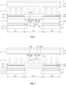
- the display panel comprises: comprises an array substrate 3, a color film substrate 5 arranged oppositely to the array substrate, a liquid crystal layer 4 between the array substrate 3 and the color film substrate 5, and a backlight module 1 positioned at a side of the color film substrate 3, which is back on to the array substrate 4.
- the display panel comprises a plurality of micro LED lighting units 303 in the first pixel area 100. A transparent area is placed among the micro LED lighting units 303.
- the color film substrate 1 comprises a color filter 305 in the second pixel area 200.
- the color film substrate could combine the micro LED display technique with the LCD display technique to accomplish the LCD full-screen design. Furthermore, there is a transparent area between two adjacent micro LED lighting units, and the transparent area could allow the light to pass through. Therefore, the in-screen sensing integration could be accomplished within the first pixel area 100.
- the present invention puts the color film substrate and the array substrate reversely when the LCD cell is formed. This makes the micro LED lighting unit, which originally uses its electrode surface as the light-emitting surface, change to use its substrate surface as the light-emitting surface. This could increase the lighting efficiency and solve the above-mentioned issue of low lighting efficiency caused by using the electrode surface of the micro LED light unit as the light-emitting surface.
- the display panel from the bottom to the top, comprises a back light module 1, a lower polarizer 2, a color film substrate 3, a LC layer 4, an array substrate 5, and an upper polarizer 6.
- the color film substrate 3 comprises: a first substrate 301, a first driving circuit 302, a plurality of micro LED lighting units 303, a planarized layer 304, a color filter 305, a black matrix 306, and an over-coating (OC) glue layer 307.
- the first substrate could be a glass substrate or a flexible substrate having a higher transparency.
- the first driving circuit 302 is placed on a surface of the first substrate 301, which is close to the LC layer 4 and the position of the first driving circuit 302 corresponds to the first pixel area 100.
- the first driving circuit 302 is used to provide a driving signal to the micro LED lighting units 303 such that the micro LED lighting unit 303 could generate light.
- the micro LED lighting units 303 are placed on a surface of the first substrate 301, which is close to the LC layer 4 and the micro LED lighting units 303 are electrically connected to the first driving circuit 302.
- the planarized layer 304 is placed on the micro LED lighting units 303 and the first substrate.
- the planarized layer 304 is used to planarize the surface of the substrate, which is used to form the micro LED lighting units 303.
- the color filter 305 is placed on the planarized layer 304 and its position is corresponding to the second pixel area 200.
- the black matrix 306 is placed between two adjacent color filters 305.
- the OC glue layer 307 is placed on the color filter 305 and the black matrix 306.
- the OC glue layer 307 could planarize the surface of the color film substrate 3.
- the first driving circuit 302 comprises scan lines (not shown) and data lines (not shown), where the scan lines extend horizontally and the data lines extend vertically. Two adjacent scan lines and two adjacent data lines define a sub-pixel area. The scan lines and the data lines could also extend to the second pixel area 200. It could be understood that the data lines and the scan lines in the second pixel area 200 may avoid the location of the color filter 305 but could correspond to the location of the black matrix 306 such that the display effect of the second pixel area 200 will not be affected.
- the first driving circuit 302 could adopt the active matrix (AM) driving technique. That is, the first driving circuit 302 further comprises TFTs (not shown). Each of the micro LED lighting units 303 is electrically connected to a corresponding scan line and a corresponding to a data line through a corresponding TFT.
- AM active matrix
- the first driving circuit 302 adopts the passive matrix (PM) driving technique. That is, the first driving circuit 302 does not have any TFT.
- PM passive matrix
- the micro LED lighting units 303 supports three-color display. That is, the micro LED lighting units 303 comprises red lighting units, green lighting units and blue lighting units.
- the size of the micro LED lighting unit 303 is 1 ⁇ m-100 ⁇ m and the height of the micro LED lighting unit 303 is 1 ⁇ m-20 ⁇ m.
- the micro LED lighting unit 303 could use its substrate surface or its electrode surface as the light-emitting surface and these changes both falls within the scope of this present invention.
- the micro LED lighting unit 303 adopts the blue display with color conversion scheme. That is, the red lighting unit comprises a blue lighting unit and a color converting layer, which could convert the blue light from the blue lighting unit into the red light.
- the green lighting unit comprises a blue lighting unit and a color converting layer, which could convert the blue light from the blue lighting unit into the green light.
- the color converting layer could be a quantum dots film or phosphor and these changes both falls within the scope of this present invention.
- Fig. 3 is a diagram of a display panel having micro LED lighting unit according to an embodiment of the present invention. Because the micro LED lighting unit 303 has an advantage of a small size, the orthogonal projection of the micro LED lighting unit 303 on the substrate is smaller than the area of the sub-pixel area P. This makes the transparent areas 300 exist among the micro LED lighting units.
- the orthogonal projection of the micro LED lighting unit 303 on the substrate occupies 10%-50% area of the sub-pixel area to make sure that the transparent area 300 is large enough to pass light.
- the first pixel area 100 Under the condition that the first pixel area 100 could normally display an image and the covering area of each of the micro LED lighting units 303 is smaller than each of the sub-pixel area P, the light could pass through those areas not covered by the micro LED lighting units 303 in the sub-pixel area P. Therefore, if the micro LED lighting units are controlled to be turned off, the first pixel area 100 could obtain the sensed image from the under-screen sensor. In this way, the under-screen fingerprint identification, under-screen camera, under-screen face identification, under-screen distance sensing, or other under-screen sensing techniques could be accomplished.
- Fig. 4 is a diagram showing a part of the area A shown in Fig. 2 .
- the micro LED lighting unit 303 comprises the electrode surface 303a and the substrate surface 303b opposite to the electrode surface 303a.
- the first electrode 3031 is placed on the electrode surface 303a.
- the electrode surface 303a of the micro LED lighting unit 303 is facing a side of the backlight module 1.
- the lighting direction of the micro LED lighting unit 303 is from the electrode 303a to the substrate surface 303b.
- the second electrode 3032 corresponding to the first electrode 3031, is placed in the first pixel area 100 of the first substrate 301.
- the second electrode 3032 lies in the sub-pixel area.
- the micro LED lighting unit 303 and the color filter 305 are at the side of the first substrate 301, which is back on to the backlight module 1.
- the first electrode 3031 of the micro LED lighting unit 303 is electrically connected to the corresponding second electrode 3032 to accomplish the electrical connection between the micro LED lighting unit 303 and the first driving circuit 302.
- the first electrode 3031 comprises an N electrode and a P electrode oppositely arranged to the N electrode.
- the second electrode 3032 comprises an N electrode and a P electrode oppositely arranged to the N electrode.
- the N electrode of the micro LED lighting unit 303 is electrically connected to the N electrode of the first substrate 303 and the P electrode of the micro LED lighting unit 303 is electrically connected to the P electrode of the first substrate 303.
- the color film substrate 3 and the array substrate 5 are reversely placed.
- the micro LED lighting unit 303 on the color film substrate 3 changes to use its substrate surface as the light-emitting surface instead of its electrode surface. Therefore, it could effectively prevent the electrode from blocking a part of light and raise the lighting efficiency. This solves the issue of low lighting efficiency when the electrode surface of the micro LED is used as the light-emitting surface.
- the planarized layer 304 is placed in the first pixel area 100 and the second pixel area 200.
- the material of the planarized layer 304 comprises, but not limited to, an organic resin, OC glue, silica gel, and etc.
- the material of the planarized layer 304 has a good high-temperature tolerance, a good adhesion, and a good transparency.
- the thickness of the planarized layer 304 is 3 ⁇ m-200 ⁇ m.
- the planarized layer 304 could be used to planarize the step difference on the substrate, which is for the transfer link of the micro LED lighting unit 303.
- the height of the micro LED lighting unit 303 is usually 1 ⁇ m-20 ⁇ m.
- the thickness of the planarized layer could be 3 ⁇ m-100 ⁇ m.
- the transparency of the planarized layer 304 is greater than or equal to 70%.
- the array substrate 5 comprises, but not limited to, a second substrate 501 and a second driving circuit 502 placed on one side of the second substrate 501, which is facing the LC layer 4.
- the second driving circuit 502 is placed in the second display area 200. Because the second driving circuit 502 is not placed in the first pixel area 100 of the display panel, it does not affect the transparency of the first pixel area 100.
- the backlight module 1 and the lower polarizer 2 have a hole corresponding to the first pixel area 100. That is, the location of the backlight module 1 and the lower polarizer 2 avoid the location of the first pixel area.
- the backlight module 1 is a direct-lit backlight module or an edge-lit backlight module and these changes fall within the scope of the present invention.
- micro LED lighting units 303 are placed only in the first pixel area 100 of the color film substrate and the first pixel area 100 is comparatively small. Therefore, in contrast to a large area mass transfer, the small area of micro LED lighting unit needs lower cost for mass transfer and recovery. In this way, it could accomplish the micro LED display technique application in the display panel/display device and could solve the issue of low yield and high cost when the mass transfer is performed.
- Fig. 5 is a diagram of a display panel according to a second embodiment of the present invention.
- the display panel of this embodiment is similar to the display panel of the first embodiment. The difference between them is:
- the micro LED lighting units 303 in the first pixel area are placed in one side of the first substrate 301, which is close to the backlight module 1.
- the color filter 305 in the second pixel area 200 is placed on the side of the first substrate 301, which is back on to the backlight module 1.
- the first driving circuit 302 and the second electrode 3032 correspond to the first pixel area 100 and are placed at one side of the first substrate 301, which is close to the backlight module 1.
- the micro LED lighting units 303 are electrically connected to the second electrode 3032 through the first electrode 3031'.
- the first electrode 3031' extends from the electrode surface 303a of the micro LED lighting unit 303 to the position of the first substrate 3031 corresponding to the second electrode 3032 along the side surface of the micro LED lighting unit 303.
- the packaging layer 308 is used to planarize the micro LED lighting unit 303 and protect the micro LED lighting unit 303 from being damaged.
- the color film substrate 3 and the array substrate 5 are reversely placed.
- the micro LED lighting unit 303 on the color film substrate 3 changes to use its substrate surface as the light-emitting surface instead of its electrode surface. Therefore, it could effectively prevent the electrode from blocking a part of light and raise the lighting efficiency. This solves the issue of low lighting efficiency when the electrode surface of the micro LED is used as the light-emitting surface.
- Fig. 6 is a diagram of a display panel according to a third embodiment of the present invention.
- the difference between the display panel of this embodiment and the display panel of the third embodiment is:
- the micro LED lighting unit 303 is placed on a position of the array substrate 5, which is corresponding to the first pixel area 100.
- the color filim substrate 3 does not have the micro LED lighting unit 303 on a position corresponding to the first pixel area 100.
- the electrode surface 303a of the micro LED lighting unit 303 on the array substrate 5 faces the color film substrate 3 such that the micro LED lighting unit 303 uses its substrate surface 303b as the light-emitting surface.
- the array substrate 5 comprises: the second substrate 501.
- the micro LED lighting unit 303 corresponds to the first pixel area 100 and is placed on the side of the second substrate 501, which is close to the color film substrate 3.
- the second driving circuit 502 corresponds to the second pixel area 200 and is placed on the side of the second substrate 501, which is close to the color film substrate 3.
- the second electrode 3032 is placed on the position of the second substrate 501, which is corresponding to the first pixel area.
- the second electrode 3032 is correspondingly placed in the sub-pixel area of the first pixel area 100.
- the electrode surface 303a of the micro LED lighting unit 303 is electrically connected to the corresponding second electrode 3032 through the first electrode 3031'.
- the first electrode 3031' extends from the electrode surface 303a of the micro LED lighting unit 303 to the position of the second substrate 501, which is corresponding to the second electrode 3032, along the side surface of the micro LED lighting unit 303.
- the other structure of the display panel of this embodiment is similar to the display panel of the first embodiment and further illustration is omitted here.
- the color film substrate 3 and the array substrate 5 are reversely placed.
- the micro LED lighting unit 303 on the color film substrate 3 changes to use its substrate surface as the light-emitting surface instead of its electrode surface. Therefore, it could effectively prevent the electrode from blocking a part of light and raise the lighting efficiency. This solves the issue of low lighting efficiency when the electrode surface of the micro LED is used as the light-emitting surface.
- a display device is provided. Please refer to Fig. 7.
- Fig. 7 is a diagram of a display device according to an embodiment of the present invention.
- the display device comprises the above-mentioned display panel and a sensor component 7.
- the backlight module 1 has a hole, which is at a position corresponding to the first pixel area 100.
- the sensor component 7 is placed correspondingly to the hole.
- the sensor component 7 is an optical sensor, which could be used to accomplish the face identification function, the distance sensing function, or the finger identification function. All these changes fall within the scope of the present invention.
- the display panel and the display device could combine the micro LED display technique with the LCD display technique.
- the LCD full-screen panel could be realized.
- the micro LED lighting unit is small, this could raise the aperture rate of the panel and realize the in-screen sensing integrated function.
- the present invention realizes the seamless connection between the micro LED display technique and LCD display technique in both horizontal and vertical spaces and thus solves the issue where a conventional LCD panel cannot spatially overlap the optical sensor and the display in order to further meet the full-screen demand.
- the present invention puts the color film substrate and the array substrate reversely when the LCD cell is formed.
- micro LED lighting unit which originally uses its electrode surface as the light-emitting surface, change to use its substrate surface as the light-emitting surface. This could increase the lighting efficiency and solve the above-mentioned issue of low lighting efficiency caused by using the electrode surface of the micro LED light unit as the light-emitting surface.
Landscapes
- Physics & Mathematics (AREA)
- Nonlinear Science (AREA)
- General Physics & Mathematics (AREA)
- Mathematical Physics (AREA)
- Chemical & Material Sciences (AREA)
- Crystallography & Structural Chemistry (AREA)
- Optics & Photonics (AREA)
- Engineering & Computer Science (AREA)
- Microelectronics & Electronic Packaging (AREA)
- Theoretical Computer Science (AREA)
- Devices For Indicating Variable Information By Combining Individual Elements (AREA)
Applications Claiming Priority (2)
| Application Number | Priority Date | Filing Date | Title |
|---|---|---|---|
| CN202010578189.8A CN111708196A (zh) | 2020-06-23 | 2020-06-23 | 显示面板及显示装置 |
| PCT/CN2020/104795 WO2021258489A1 (fr) | 2020-06-23 | 2020-07-27 | Écran d'affichage et dispositif d'affichage |
Publications (2)
| Publication Number | Publication Date |
|---|---|
| EP4170416A1 true EP4170416A1 (fr) | 2023-04-26 |
| EP4170416A4 EP4170416A4 (fr) | 2024-08-14 |
Family
ID=79023427
Family Applications (1)
| Application Number | Title | Priority Date | Filing Date |
|---|---|---|---|
| EP20870442.9A Pending EP4170416A4 (fr) | 2020-06-23 | 2020-07-27 | Écran d'affichage et dispositif d'affichage |
Country Status (2)
| Country | Link |
|---|---|
| US (1) | US11536995B2 (fr) |
| EP (1) | EP4170416A4 (fr) |
Families Citing this family (3)
| Publication number | Priority date | Publication date | Assignee | Title |
|---|---|---|---|---|
| CN112764258B (zh) * | 2020-12-22 | 2022-06-28 | 厦门天马微电子有限公司 | 一种显示装置及其控制方法 |
| CN114415433B (zh) * | 2022-03-14 | 2022-07-12 | 惠科股份有限公司 | 阵列基板、显示面板和显示装置 |
| CN115206201B (zh) * | 2022-07-20 | 2023-11-10 | 厦门天马微电子有限公司 | 显示面板及其制备方法、显示装置 |
Family Cites Families (13)
| Publication number | Priority date | Publication date | Assignee | Title |
|---|---|---|---|---|
| US20090141004A1 (en) * | 2007-12-03 | 2009-06-04 | Semiconductor Energy Laboratory Co., Ltd. | Display device and method for manufacturing the same |
| KR101592010B1 (ko) * | 2009-07-17 | 2016-02-05 | 삼성디스플레이 주식회사 | 표시 장치 및 그 제조 방법 |
| KR101806339B1 (ko) * | 2016-06-28 | 2017-12-08 | 한국광기술원 | 투명 디스플레이용 마이크로 led의 제조방법 및 이를 이용한 투명 디스플레이용 마이크로 led |
| KR102734610B1 (ko) * | 2016-12-30 | 2024-11-25 | 엘지디스플레이 주식회사 | 액정 표시 장치 |
| US10664676B2 (en) * | 2017-06-12 | 2020-05-26 | Will Semiconductor (Shanghai) Co. Ltd. | Systems and methods for reducing unwanted reflections in display systems incorporating an under display biometric sensor |
| TWI681554B (zh) * | 2018-05-10 | 2020-01-01 | 友達光電股份有限公司 | 畫素陣列基板及其驅動方法 |
| CN108810201B (zh) | 2018-06-04 | 2020-07-17 | Oppo广东移动通信有限公司 | 电子装置及利用电子装置拍摄照片的方法 |
| CN111491077B (zh) * | 2019-01-29 | 2022-09-16 | 北京小米移动软件有限公司 | 终端、显示面板和图像采集模组以及显示控制方法 |
| CN110231735B (zh) * | 2019-05-16 | 2023-08-22 | 武汉华星光电技术有限公司 | 显示装置 |
| CN110275340A (zh) * | 2019-06-10 | 2019-09-24 | 武汉华星光电技术有限公司 | 用于屏下辨识方案的液晶显示设备 |
| CN110632789A (zh) * | 2019-08-22 | 2019-12-31 | 武汉华星光电技术有限公司 | 显示装置 |
| CN110568649A (zh) * | 2019-09-10 | 2019-12-13 | 武汉华星光电技术有限公司 | 一种显示装置及其驱动方法 |
| CN110794604A (zh) * | 2019-11-29 | 2020-02-14 | 武汉华星光电技术有限公司 | 显示装置及显示装置的制作方法 |
-
2020
- 2020-07-27 EP EP20870442.9A patent/EP4170416A4/fr active Pending
- 2020-07-27 US US16/981,761 patent/US11536995B2/en active Active
Also Published As
| Publication number | Publication date |
|---|---|
| EP4170416A4 (fr) | 2024-08-14 |
| US20210397054A1 (en) | 2021-12-23 |
| US11536995B2 (en) | 2022-12-27 |
Similar Documents
| Publication | Publication Date | Title |
|---|---|---|
| US11256121B2 (en) | Liquid crystal display device for under-screen identification scheme | |
| US11977292B2 (en) | Color filter substrate, display panel, and display device | |
| KR102536628B1 (ko) | 투명표시장치 | |
| US20230099140A1 (en) | Color filter substrate and display panel | |
| KR102925384B1 (ko) | 전자 장치 | |
| CN111708196A (zh) | 显示面板及显示装置 | |
| US12433125B2 (en) | Display substrate and display device | |
| CN110794604A (zh) | 显示装置及显示装置的制作方法 | |
| CN108267903A (zh) | 显示装置、使用其的多屏幕显示装置及其制造方法 | |
| CN212276177U (zh) | 一种彩膜基板和显示面板 | |
| KR102941804B1 (ko) | 마이크로 led를 이용한 디스플레이 장치 | |
| US12055825B2 (en) | Display device | |
| US11536995B2 (en) | Display panel and display device | |
| CN111370461A (zh) | 显示面板和显示装置 | |
| US20220350193A1 (en) | Display panel and display device | |
| CN112951106A (zh) | 显示装置 | |
| US10429700B2 (en) | Display module and display device | |
| CN103713418A (zh) | 滤色器基板、电光装置及电子设备 | |
| CN116390596A (zh) | 显示面板和显示装置 | |
| CN212276178U (zh) | 一种彩膜基板、显示面板、显示装置 | |
| US20220013596A1 (en) | Display panel and display device including the same | |
| CN216980563U (zh) | 一种透明显示器件及展柜 | |
| US20260107663A1 (en) | Adhesive member of display device, electronic device having the same, and method providing the same | |
| EP4665122A1 (fr) | Dispositif d'affichage | |
| EP4513558A1 (fr) | Dispositif d'affichage utilisant un élément électroluminescent |
Legal Events
| Date | Code | Title | Description |
|---|---|---|---|
| STAA | Information on the status of an ep patent application or granted ep patent |
Free format text: STATUS: UNKNOWN |
|
| STAA | Information on the status of an ep patent application or granted ep patent |
Free format text: STATUS: THE INTERNATIONAL PUBLICATION HAS BEEN MADE |
|
| PUAI | Public reference made under article 153(3) epc to a published international application that has entered the european phase |
Free format text: ORIGINAL CODE: 0009012 |
|
| STAA | Information on the status of an ep patent application or granted ep patent |
Free format text: STATUS: REQUEST FOR EXAMINATION WAS MADE |
|
| 17P | Request for examination filed |
Effective date: 20210407 |
|
| AK | Designated contracting states |
Kind code of ref document: A1 Designated state(s): AL AT BE BG CH CY CZ DE DK EE ES FI FR GB GR HR HU IE IS IT LI LT LU LV MC MK MT NL NO PL PT RO RS SE SI SK SM TR |
|
| DAV | Request for validation of the european patent (deleted) | ||
| DAX | Request for extension of the european patent (deleted) | ||
| A4 | Supplementary search report drawn up and despatched |
Effective date: 20240712 |
|
| RIC1 | Information provided on ipc code assigned before grant |
Ipc: G09F 9/33 20060101ALI20240709BHEP Ipc: G02F 1/1362 20060101ALI20240709BHEP Ipc: G02F 1/13357 20060101ALI20240709BHEP Ipc: G02F 1/1335 20060101ALI20240709BHEP Ipc: G02F 1/1333 20060101AFI20240709BHEP |
|
| STAA | Information on the status of an ep patent application or granted ep patent |
Free format text: STATUS: EXAMINATION IS IN PROGRESS |
|
| 17Q | First examination report despatched |
Effective date: 20260107 |