EP4170488A1 - Procédé de commande d'activation de puce, puce, écran et dispositif électronique - Google Patents
Procédé de commande d'activation de puce, puce, écran et dispositif électronique Download PDFInfo
- Publication number
- EP4170488A1 EP4170488A1 EP21826428.1A EP21826428A EP4170488A1 EP 4170488 A1 EP4170488 A1 EP 4170488A1 EP 21826428 A EP21826428 A EP 21826428A EP 4170488 A1 EP4170488 A1 EP 4170488A1
- Authority
- EP
- European Patent Office
- Prior art keywords
- chip
- booting
- booting information
- information
- preset condition
- Prior art date
- Legal status (The legal status is an assumption and is not a legal conclusion. Google has not performed a legal analysis and makes no representation as to the accuracy of the status listed.)
- Granted
Links
Images


Classifications
-
- G—PHYSICS
- G06—COMPUTING OR CALCULATING; COUNTING
- G06F—ELECTRIC DIGITAL DATA PROCESSING
- G06F21/00—Security arrangements for protecting computers, components thereof, programs or data against unauthorised activity
- G06F21/50—Monitoring users, programs or devices to maintain the integrity of platforms, e.g. of processors, firmware or operating systems
- G06F21/57—Certifying or maintaining trusted computer platforms, e.g. secure boots or power-downs, version controls, system software checks, secure updates or assessing vulnerabilities
- G06F21/575—Secure boot
-
- G—PHYSICS
- G06—COMPUTING OR CALCULATING; COUNTING
- G06F—ELECTRIC DIGITAL DATA PROCESSING
- G06F9/00—Arrangements for program control, e.g. control units
- G06F9/06—Arrangements for program control, e.g. control units using stored programs, i.e. using an internal store of processing equipment to receive or retain programs
- G06F9/44—Arrangements for executing specific programs
- G06F9/4401—Bootstrapping
- G06F9/4411—Configuring for operating with peripheral devices; Loading of device drivers
-
- G—PHYSICS
- G06—COMPUTING OR CALCULATING; COUNTING
- G06F—ELECTRIC DIGITAL DATA PROCESSING
- G06F9/00—Arrangements for program control, e.g. control units
- G06F9/06—Arrangements for program control, e.g. control units using stored programs, i.e. using an internal store of processing equipment to receive or retain programs
- G06F9/44—Arrangements for executing specific programs
- G06F9/4401—Bootstrapping
- G06F9/4406—Loading of operating system
- G06F9/4408—Boot device selection
-
- G—PHYSICS
- G06—COMPUTING OR CALCULATING; COUNTING
- G06F—ELECTRIC DIGITAL DATA PROCESSING
- G06F1/00—Details not covered by groups G06F3/00 - G06F13/00 and G06F21/00
- G06F1/24—Resetting means
-
- G—PHYSICS
- G06—COMPUTING OR CALCULATING; COUNTING
- G06F—ELECTRIC DIGITAL DATA PROCESSING
- G06F11/00—Error detection; Error correction; Monitoring
- G06F11/07—Responding to the occurrence of a fault, e.g. fault tolerance
- G06F11/08—Error detection or correction by redundancy in data representation, e.g. by using checking codes
- G06F11/10—Adding special bits or symbols to the coded information, e.g. parity check, casting out 9's or 11's
-
- G—PHYSICS
- G06—COMPUTING OR CALCULATING; COUNTING
- G06F—ELECTRIC DIGITAL DATA PROCESSING
- G06F11/00—Error detection; Error correction; Monitoring
- G06F11/07—Responding to the occurrence of a fault, e.g. fault tolerance
- G06F11/08—Error detection or correction by redundancy in data representation, e.g. by using checking codes
- G06F11/10—Adding special bits or symbols to the coded information, e.g. parity check, casting out 9's or 11's
- G06F11/1004—Adding special bits or symbols to the coded information, e.g. parity check, casting out 9's or 11's to protect a block of data words, e.g. CRC or checksum
-
- G—PHYSICS
- G06—COMPUTING OR CALCULATING; COUNTING
- G06F—ELECTRIC DIGITAL DATA PROCESSING
- G06F9/00—Arrangements for program control, e.g. control units
- G06F9/06—Arrangements for program control, e.g. control units using stored programs, i.e. using an internal store of processing equipment to receive or retain programs
- G06F9/44—Arrangements for executing specific programs
- G06F9/4401—Bootstrapping
-
- G—PHYSICS
- G06—COMPUTING OR CALCULATING; COUNTING
- G06F—ELECTRIC DIGITAL DATA PROCESSING
- G06F9/00—Arrangements for program control, e.g. control units
- G06F9/06—Arrangements for program control, e.g. control units using stored programs, i.e. using an internal store of processing equipment to receive or retain programs
- G06F9/44—Arrangements for executing specific programs
- G06F9/4401—Bootstrapping
- G06F9/4418—Suspend and resume; Hibernate and awake
-
- G—PHYSICS
- G06—COMPUTING OR CALCULATING; COUNTING
- G06F—ELECTRIC DIGITAL DATA PROCESSING
- G06F9/00—Arrangements for program control, e.g. control units
- G06F9/06—Arrangements for program control, e.g. control units using stored programs, i.e. using an internal store of processing equipment to receive or retain programs
- G06F9/44—Arrangements for executing specific programs
- G06F9/445—Program loading or initiating
-
- G—PHYSICS
- G09—EDUCATION; CRYPTOGRAPHY; DISPLAY; ADVERTISING; SEALS
- G09G—ARRANGEMENTS OR CIRCUITS FOR CONTROL OF INDICATING DEVICES USING STATIC MEANS TO PRESENT VARIABLE INFORMATION
- G09G3/00—Control arrangements or circuits, of interest only in connection with visual indicators other than cathode-ray tubes
- G09G3/20—Control arrangements or circuits, of interest only in connection with visual indicators other than cathode-ray tubes for presentation of an assembly of a number of characters, e.g. a page, by composing the assembly by combination of individual elements arranged in a matrix no fixed position being assigned to or needed to be assigned to the individual characters or partial characters
-
- G—PHYSICS
- G09—EDUCATION; CRYPTOGRAPHY; DISPLAY; ADVERTISING; SEALS
- G09G—ARRANGEMENTS OR CIRCUITS FOR CONTROL OF INDICATING DEVICES USING STATIC MEANS TO PRESENT VARIABLE INFORMATION
- G09G5/00—Control arrangements or circuits for visual indicators common to cathode-ray tube indicators and other visual indicators
- G09G5/36—Control arrangements or circuits for visual indicators common to cathode-ray tube indicators and other visual indicators characterised by the display of a graphic pattern, e.g. using an all-points-addressable [APA] memory
-
- H—ELECTRICITY
- H04—ELECTRIC COMMUNICATION TECHNIQUE
- H04L—TRANSMISSION OF DIGITAL INFORMATION, e.g. TELEGRAPHIC COMMUNICATION
- H04L63/00—Network architectures or network communication protocols for network security
- H04L63/08—Network architectures or network communication protocols for network security for authentication of entities
- H04L63/083—Network architectures or network communication protocols for network security for authentication of entities using passwords
- H04L63/0838—Network architectures or network communication protocols for network security for authentication of entities using passwords using one-time-passwords
-
- G—PHYSICS
- G06—COMPUTING OR CALCULATING; COUNTING
- G06F—ELECTRIC DIGITAL DATA PROCESSING
- G06F21/00—Security arrangements for protecting computers, components thereof, programs or data against unauthorised activity
- G06F21/30—Authentication, i.e. establishing the identity or authorisation of security principals
- G06F21/44—Program or device authentication
-
- G—PHYSICS
- G06—COMPUTING OR CALCULATING; COUNTING
- G06F—ELECTRIC DIGITAL DATA PROCESSING
- G06F21/00—Security arrangements for protecting computers, components thereof, programs or data against unauthorised activity
- G06F21/50—Monitoring users, programs or devices to maintain the integrity of platforms, e.g. of processors, firmware or operating systems
- G06F21/51—Monitoring users, programs or devices to maintain the integrity of platforms, e.g. of processors, firmware or operating systems at application loading time, e.g. accepting, rejecting, starting or inhibiting executable software based on integrity or source reliability
-
- G—PHYSICS
- G06—COMPUTING OR CALCULATING; COUNTING
- G06F—ELECTRIC DIGITAL DATA PROCESSING
- G06F21/00—Security arrangements for protecting computers, components thereof, programs or data against unauthorised activity
- G06F21/60—Protecting data
- G06F21/64—Protecting data integrity, e.g. using checksums, certificates or signatures
-
- G—PHYSICS
- G06—COMPUTING OR CALCULATING; COUNTING
- G06F—ELECTRIC DIGITAL DATA PROCESSING
- G06F2201/00—Indexing scheme relating to error detection, to error correction, and to monitoring
- G06F2201/81—Threshold
-
- G—PHYSICS
- G06—COMPUTING OR CALCULATING; COUNTING
- G06F—ELECTRIC DIGITAL DATA PROCESSING
- G06F9/00—Arrangements for program control, e.g. control units
- G06F9/06—Arrangements for program control, e.g. control units using stored programs, i.e. using an internal store of processing equipment to receive or retain programs
- G06F9/44—Arrangements for executing specific programs
- G06F9/4401—Bootstrapping
- G06F9/4403—Processor initialisation
-
- G—PHYSICS
- G06—COMPUTING OR CALCULATING; COUNTING
- G06F—ELECTRIC DIGITAL DATA PROCESSING
- G06F9/00—Arrangements for program control, e.g. control units
- G06F9/06—Arrangements for program control, e.g. control units using stored programs, i.e. using an internal store of processing equipment to receive or retain programs
- G06F9/44—Arrangements for executing specific programs
- G06F9/4401—Bootstrapping
- G06F9/4406—Loading of operating system
-
- G—PHYSICS
- G09—EDUCATION; CRYPTOGRAPHY; DISPLAY; ADVERTISING; SEALS
- G09G—ARRANGEMENTS OR CIRCUITS FOR CONTROL OF INDICATING DEVICES USING STATIC MEANS TO PRESENT VARIABLE INFORMATION
- G09G2330/00—Aspects of power supply; Aspects of display protection and defect management
- G09G2330/02—Details of power systems and of start or stop of display operation
- G09G2330/026—Arrangements or methods related to booting a display
-
- G—PHYSICS
- G09—EDUCATION; CRYPTOGRAPHY; DISPLAY; ADVERTISING; SEALS
- G09G—ARRANGEMENTS OR CIRCUITS FOR CONTROL OF INDICATING DEVICES USING STATIC MEANS TO PRESENT VARIABLE INFORMATION
- G09G2360/00—Aspects of the architecture of display systems
- G09G2360/12—Frame memory handling
- G09G2360/121—Frame memory handling using a cache memory
-
- Y—GENERAL TAGGING OF NEW TECHNOLOGICAL DEVELOPMENTS; GENERAL TAGGING OF CROSS-SECTIONAL TECHNOLOGIES SPANNING OVER SEVERAL SECTIONS OF THE IPC; TECHNICAL SUBJECTS COVERED BY FORMER USPC CROSS-REFERENCE ART COLLECTIONS [XRACs] AND DIGESTS
- Y02—TECHNOLOGIES OR APPLICATIONS FOR MITIGATION OR ADAPTATION AGAINST CLIMATE CHANGE
- Y02D—CLIMATE CHANGE MITIGATION TECHNOLOGIES IN INFORMATION AND COMMUNICATION TECHNOLOGIES [ICT], I.E. INFORMATION AND COMMUNICATION TECHNOLOGIES AIMING AT THE REDUCTION OF THEIR OWN ENERGY USE
- Y02D10/00—Energy efficient computing, e.g. low power processors, power management or thermal management
Definitions
- the present disclosure relates to the field of chip technology, and in particular, to a chip booting control method, a chip, a display panel, and an electronic apparatus.
- the chip is first initialized in order to make the chip work normally, and the initialization process may include loading a program of the chip and configuring parameters in the chip, etc.
- a series of parameters need to be configured upon chip booting to ensure that the chip can function normally.
- the existing chip booting flow is as follows: after chip power-on booting or chip reset is completed, a firmware saved in a flash memory is loaded into a static random access memory (SRAM), and if there is no flash memory, a firmware is loaded from an external control unit.
- SRAM static random access memory
- the present disclosure provides a chip booting control method, the method being applied to a control module of a chip, the chip further comprising a buffer module, the method comprising:
- determining whether the first booting information satisfies the first preset condition comprises:
- determining the verification result corresponding to the first booting information comprises: determining, based on the first booting information, the verification result corresponding to the first booting information by a cyclic redundancy check algorithm or a parity check algorithm.
- the method further comprising: loading second booting information for chip booting into the buffer module in response to the first booting information not satisfying the first preset condition.
- the method further comprising: after the chip is booted, altering or erasing the pre-stored verification code stored in the buffer module based on a second preset condition.
- a chip comprising a control module and a buffer module, wherein the control module is configured to:
- control module determining whether the first booting information satisfies the first preset condition comprises:
- control module determining the verification result corresponding to the first booting information comprises: determining, based on the first booting information, the verification result corresponding to the first booting information by a cyclic redundancy check algorithm or a parity check algorithm.
- the chip further comprising a storage module
- the control module is further configured to: loading second booting information for chip booting in the storage module into the buffer module in response to the first booting information not satisfying the first preset condition.
- control module is further configured to: after the chip is booted, alter or erase the pre-stored verification code stored in the buffer module based on a second preset condition.
- a display panel comprising: a display component; and the above chip.
- the display component comprises at least one of a liquid crystal display component, a light emitting diode display component, an organic light emitting diode display component, or OLED display component.
- a chip of an embodiment of the present disclosure may comprise a touch chip, which may be applied to a touch terminal. It should be noted that embodiments of the present disclosure do not limit the type of the chip.
- the buffer module of the embodiment of the present disclosure may comprise a memory.
- the memory may include a random access memory (RAM), which may store information to a designated unit and read information from the designated unit, and a read only memory (ROM), which may fixedly store data.
- RAM random access memory
- ROM read only memory
- the buffer module of the embodiment of the present disclosure may include a static random access memory (SRAM). It should be noted that embodiments of the present disclosure do not limit the type of the buffer module.
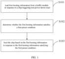
- Fig. 1 shows a schematic flowchart of a chip booting control method according to an embodiment of the present disclosure.
- the chip booting control method implemented in accordance with the present disclosure may be applied to a control module of the chip. As shown in Fig.1 , the method comprises:
- a firmware (codes) saved in a storage module e.g., a flash memory
- an external control unit may be pre-stored into the buffer module at chip booting or power-down reset; and the codes for chip booting pre-stored in the buffer module may not be lost or corrupted when the chip triggers non-power-down reset, for example, through a chip reset pin or triggering a watchdog reset.
- step S101 first booting information is read from the buffer module in response to the chip triggering non-power-down reset.
- the first booting information is used to boot the chip.
- the first booting information may include codes required for chip booting; the first booting information may include binary codes; and the type and form of the first booting information is not limited by embodiments of the present disclosure.
- the chip triggers non-power-down reset, the booting information may not be lost or corrupted, in which case the first booting information currently buffered in the buffer module may be checked.
- the first preset condition comprises whether the first booting information has an enabling flag, whether a length of the first booting information is greater than a preset threshold value, and whether a check result (verification result) corresponding to the first booting information is the same as a pre-stored check code (verification code) in the buffer module.
- the enabling flag may include a binary sequence. Exemplarily, taking an enabling flag of 0001 as an example, if the first four bits of the first booting information are 0001, the first booting information may be deemed as having an enabling flag. It should be noted that embodiments of the present disclosure do not limit the specific value of the enabling flag and the position of the enabling flag in the code.
- the pre-stored check code is used to indicate check information (verification information) of second booting information loaded in the buffer module.
- codes for chip booting are often fixed, and the check code corresponding to the codes for chip booting is fixed as well, so that the check code corresponding to the codes for chip booting can be stored as a pre-stored check code in the buffer module.
- step S103 in a case where the first booting information satisfies the first preset condition, the booting information currently buffered in the buffer module can be deemed intact, and the chip can be booted directly without reloading the booting information into the buffer module.
- the method of an embodiment of the present disclosure further comprises: loading second booting information for chip booting into the buffer module in response to the first booting information not satisfying the first preset condition.
- the second booting information may be stored in a storage module.
- the storage module may include a non-volatile storage medium, for example, a flash memory (FLASH), an EEPROM (Electrically Erasable Programmable Read Only Memory), a MRAM (Magnetic Random Access Memory), or a FeRAM (Fe Random Access Memory).
- FLASH flash memory
- EEPROM Electrically Erasable Programmable Read Only Memory
- MRAM Magnetic Random Access Memory
- FeRAM Fe Random Access Memory
- the second booting information is used to boot the chip, and may include correct codes for chip booting, and when the first booting information satisfies the first preset condition, contents contained in the first booting information and the second booting information are the same.
- the booting information pre-stored in the buffer module may be deemed missing or corrupted, then the second booting information stored in the storage module may be loaded into the buffer module, such that the chip is booted normally.
- Loading the correct codes for chip booting into the buffer module in a case where the booting information does not satisfy the first preset condition allows ensuring normal booting of the chip even when the booting information is corrupted or lost, which improves fault tolerance of the method of embodiments of the present disclosure.
- the method of an embodiment of the present disclosure further comprises: altering or erasing the pre-stored check code stored in the buffer module according to a second preset condition, after the chip is booted.
- the second preset condition may include altering the pre-stored check code stored in the buffer module on a preset period, or erasing the pre-stored check code stored in the buffer module at one-time, according to user requirements.
- Fig.2 shows a schematic flowchart of a method for booting a chip according to first booting information implemented in accordance with the present disclosure. As shown in Fig.2 , the method for booting a chip according to first booting information comprises:
- the first booting information has an enabling flag and determining whether the length of the first booting information is greater than a preset threshold value, it can be determined whether the first booting information is severely corrupted in a case where the chip trigger non-power-down reset and, if so, reloading the correct codes for chip booting is required.
- the specific value of the preset threshold value may be set according to user requirements.
- the preset threshold value may be zero, and the present embodiment is not limited thereto.
- the first booting information and the pre-stored check code may be stored in different positions in the buffer module, and that the first booting information and the pre-stored check code may be in different forms.
- determining the check result corresponding to the first booting information comprises: determining, according to the first booting information, a check result corresponding to the first booting information by a cyclic redundancy check algorithm or a parity check algorithm.
- determining, by the cyclic redundancy check algorithm, the check result corresponding to the first booting information may comprise: performing a division operation of dividing the first booting information with a predetermined divisor (e.g., 10011); determining a remainder corresponding to the division operation; complementing the remainder after the data of the first booting information; and using a result of complementing the remainder after the data of the first booting as a check result corresponding to the first booting information.
- a predetermined divisor e.g. 10011
- the parity check algorithm may include odd check and even check.
- the odd check may complement 0 after the data of the first booting information, then the check result corresponding to the first booting information is 000110100, and the number of 1s in the check result is odd (3);
- the even check may complement 1 after the data of the first booting information, then the check result corresponding to the first booting information is 000110101, and the number of 1s in the check result is even (4).
- the check result corresponding to the first booting information is determined through the parity check algorithm, whether the check result is the same as the pre-stored check code in the buffer module can be determined by determining whether the number of 1s in the check result is the same as the number of 1s in the pre-stored check code.
- the chip booting control method of an embodiment of the present disclosure is capable of booting the chip according to codes for chip booting pre-stored in the buffer module when the check code satisfies the first preset condition in a case of non-power-down reset, which eliminates the time for reloading the codes for chip booting to the buffer module and saves the time for chip booting.
- the check code stored in the buffer module can be altered or erased according to user requirements, so as to meet personalized needs of the user.
- Fig. 3 shows a schematic diagram of device structure of a chip implemented in accordance with the present disclosure.
- the device may comprise:
- control module 31 determining the check result corresponding to the first booting information comprises: determining, according to the first booting information, a check result corresponding to the first booting information by a cyclic redundancy check algorithm or a parity check algorithm.
- the chip further comprises a storage module
- the control module 31 is further configured to: load second booting information for chip booting in the storage module into the buffer module 32 in response to the first booting information not satisfying the first preset condition.
- control module 31 is further configured to: alter or erase the pre-stored check code stored in the buffer module 32 according to the second preset condition, after the chip is booted.
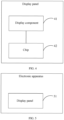
- Fig. 4 shows a structural schematic diagram of a display panel implemented in accordance with the present disclosure.
- the display panel may comprise:
- the display component 41 comprises at least one of a liquid crystal display component, a light emitting diode display component, an organic light emitting diode display component, or an OLED (Organic Light Emitting Diode) display component.
- the display component 41 may comprise a liquid crystal display (LCD) and a touch panel (TP). If the display component 41 comprises a touch panel, the display component 41 may be implemented as a touch screen to receive input signals from a user.
- the touch panel includes one or more touch sensors to sense touch, swipes, and gestures on the touch panel. The touch sensor may not only sense the boundary of a touch or swipe action, but also detect the duration and pressure associated with the touch or swipe operation.
- Fig. 5 shows a structural schematic diagram of an electronic apparatus implemented in accordance with the present disclosure.
- the electronic apparatus may comprise: the display panel in the corresponding embodiment as shown in Fig. 5 .
- the present disclosure may be implemented by a system, a method, and/or a computer program product.
- the computer program product may include a computer readable storage medium having computer readable program instructions for causing a processor to carry out the aspects of the present disclosure stored thereon.
- the computer readable storage medium can be a tangible device that can retain and store instructions used by an instruction executing device.
- the computer readable storage medium may be, but not limited to, e.g., electronic storage device, magnetic storage device, optical storage device, electromagnetic storage device, semiconductor storage device, or any proper combination thereof.
- a non-exhaustive list of more specific examples of the computer readable storage medium includes: portable computer diskette, hard disk, random access memory (RAM), read-only memory (ROM), erasable programmable read-only memory (EPROM or Flash memory), static random access memory (SRAM), portable compact disc read-only memory (CD-ROM), digital versatile disk (DVD), memory stick, floppy disk, mechanically encoded device (for example, punch-cards or raised structures in a groove having instructions recorded thereon), and any proper combination thereof.
- RAM random access memory
- ROM read-only memory
- EPROM or Flash memory erasable programmable read-only memory
- SRAM static random access memory
- CD-ROM compact disc read-only memory
- DVD digital versatile disk
- memory stick floppy disk
- mechanically encoded device for example, punch-cards or raised structures in a groove having instructions recorded thereon
- a computer readable storage medium referred herein should not to be construed as transitory signal per se, such as radio waves or other freely propagating electromagnetic waves, electromagnetic waves propagating through a waveguide or other transmission media (e.g., light pulses passing through a fiber-optic cable), or electrical signal transmitted through a wire.
- Computer readable program instructions described herein can be downloaded to individual computing/processing devices from a computer readable storage medium or to an external computer or external storage device via network, for example, the Internet, local area network, wide area network and/or wireless network.
- the network may comprise copper transmission cables, optical transmission fibers, wireless transmission, routers, firewalls, switches, gateway computers and/or edge servers.
- a network adapter card or network interface in each computing/processing device receives computer readable program instructions from the network and forwards the computer readable program instructions for storage in a computer readable storage medium in the respective computing/processing devices.
- Computer readable program instructions for carrying out the operations of the present disclosure may be assembler instructions, instruction-set-architecture (ISA) instructions, machine instructions, machine-related instructions, microcode, firmware instructions, state-setting data, or source code or object code written in any combination of one or more programming languages.
- the programming languages include an object oriented programming language, such as Smalltalk, C++ or the like, and the conventional procedural programming languages, such as the "C" programming language or similar programming languages.
- the computer readable program instructions may be executed completely on the user's computer, partly on the user's computer, as a stand-alone software package, partly on the user's computer and partly on a remote computer, or completely on a remote computer or a server.
- the remote computer may be connected to the user's computer through any type of network, including local area network (LAN) or wide area network (WAN), or connected to an external computer (for example, through the Internet connection from an Internet Service Provider).
- electronic circuitry such as programmable logic circuitry, field-programmable gate arrays (FPGA), or programmable logic arrays (PLA), may be customized from state information of the computer readable program instructions; the electronic circuitry may execute the computer readable program instructions, so as to achieve the aspects of the present disclosure.
- These computer readable program instructions may be provided to a processor of a general purpose computer, a dedicated computer, or other programmable data processing devices, to produce a machine, such that the instructions create means for implementing the functions/acts specified in one or more blocks in the flowchart and/or block diagram when executed by the processor of the computer or other programmable data processing devices.
- These computer readable program instructions may also be stored in a computer readable storage medium, wherein the instructions cause a computer, a programmable data processing device and/or other devices to function in a particular manner, such that the computer readable storage medium having instructions stored therein comprises a product that includes instructions implementing aspects of the functions/acts specified in one or more blocks in the flowchart and/or block diagram.
- the computer readable program instructions may also be loaded onto a computer, other programmable data processing devices, or other devices to have a series of operational steps performed on the computer, other programmable devices or other devices, so as to produce a computer implemented process, such that the instructions executed on the computer, other programmable devices or other devices implement the functions/acts specified in one or more blocks in the flowchart and/or block diagram.
- each block in the flowchart or block diagram may represent a part of a module, a program segment, or a portion of code, which comprises one or more executable instructions for implementing the specified logical function(s).
- the functions denoted in the blocks may occur in an order different from that denoted in the drawings. For example, two contiguous blocks may, in fact, be executed substantially concurrently, or sometimes they may be executed in a reverse order, depending upon the functions involved.
- each block in the block diagram and/or flowchart, and combinations of blocks in the block diagram and/or flowchart can be implemented by dedicated hardware-based systems performing the specified functions or acts, or by combinations of dedicated hardware and computer instructions.
Landscapes
- Engineering & Computer Science (AREA)
- Theoretical Computer Science (AREA)
- Software Systems (AREA)
- General Physics & Mathematics (AREA)
- General Engineering & Computer Science (AREA)
- Physics & Mathematics (AREA)
- Computer Security & Cryptography (AREA)
- Computer Hardware Design (AREA)
- Quality & Reliability (AREA)
- Computing Systems (AREA)
- Signal Processing (AREA)
- Computer Networks & Wireless Communication (AREA)
- Stored Programmes (AREA)
- Memory System Of A Hierarchy Structure (AREA)
- Retry When Errors Occur (AREA)
Applications Claiming Priority (2)
| Application Number | Priority Date | Filing Date | Title |
|---|---|---|---|
| CN202010566789.2A CN111722878A (zh) | 2020-06-19 | 2020-06-19 | 芯片启动控制方法、芯片、显示面板及电子设备 |
| PCT/CN2021/091039 WO2021254003A1 (fr) | 2020-06-19 | 2021-04-29 | Procédé de commande d'activation de puce, puce, écran et dispositif électronique |
Publications (4)
| Publication Number | Publication Date |
|---|---|
| EP4170488A1 true EP4170488A1 (fr) | 2023-04-26 |
| EP4170488A4 EP4170488A4 (fr) | 2023-11-29 |
| EP4170488C0 EP4170488C0 (fr) | 2024-10-09 |
| EP4170488B1 EP4170488B1 (fr) | 2024-10-09 |
Family
ID=72567779
Family Applications (1)
| Application Number | Title | Priority Date | Filing Date |
|---|---|---|---|
| EP21826428.1A Active EP4170488B1 (fr) | 2020-06-19 | 2021-04-29 | Procédé de commande d'activation de puce, puce, écran et dispositif électronique |
Country Status (6)
| Country | Link |
|---|---|
| US (1) | US11960902B2 (fr) |
| EP (1) | EP4170488B1 (fr) |
| JP (1) | JP7482261B2 (fr) |
| KR (1) | KR102774859B1 (fr) |
| CN (1) | CN111722878A (fr) |
| WO (1) | WO2021254003A1 (fr) |
Families Citing this family (5)
| Publication number | Priority date | Publication date | Assignee | Title |
|---|---|---|---|---|
| CN111722878A (zh) * | 2020-06-19 | 2020-09-29 | 北京集创北方科技股份有限公司 | 芯片启动控制方法、芯片、显示面板及电子设备 |
| CN114661368B (zh) * | 2022-05-19 | 2022-09-06 | 中昊芯英(杭州)科技有限公司 | 一种芯片及其启动方法 |
| CN115080144A (zh) * | 2022-06-15 | 2022-09-20 | 中昊芯英(杭州)科技有限公司 | 一种芯片启动装置及方法 |
| CN115658183B (zh) * | 2022-12-26 | 2023-03-31 | 北京紫光芯能科技有限公司 | 用于控制mcu的方法及装置、电子设备、存储介质 |
| CN116719583B (zh) * | 2023-08-08 | 2023-11-10 | 飞腾信息技术有限公司 | 一种启动方法、可编程逻辑器件、计算设备及存储介质 |
Family Cites Families (22)
| Publication number | Priority date | Publication date | Assignee | Title |
|---|---|---|---|---|
| US7761653B2 (en) * | 1999-08-04 | 2010-07-20 | Super Talent Electronics, Inc. | Flash micro-controller with shadow boot-loader SRAM for dual-device booting of micro-controller and host |
| JP3845258B2 (ja) * | 2000-12-19 | 2006-11-15 | 株式会社リコー | モデム装置及び通信端末装置 |
| US7594135B2 (en) * | 2003-12-31 | 2009-09-22 | Sandisk Corporation | Flash memory system startup operation |
| US7921303B2 (en) * | 2005-11-18 | 2011-04-05 | Qualcomm Incorporated | Mobile security system and method |
| US7490177B2 (en) * | 2006-01-23 | 2009-02-10 | Infineon Technologies Ag | System method for performing a direct memory access for automatically copying initialization boot code in a new memory architecture |
| CN101957762A (zh) * | 2009-07-15 | 2011-01-26 | 鸿富锦精密工业(深圳)有限公司 | 加速启动装置、具有该装置的计算机系统及其启动方法 |
| US8719559B2 (en) * | 2010-10-13 | 2014-05-06 | International Business Machines Corporation | Memory tagging and preservation during a hot upgrade |
| CN102169442B (zh) * | 2011-03-24 | 2014-09-10 | 杭州华三通信技术有限公司 | 使用usb设备进行系统引导的方法、设备、装置及系统 |
| CN102855145B (zh) * | 2011-06-30 | 2015-07-01 | 安凯(广州)微电子技术有限公司 | 嵌入式电子设备启动方法及系统 |
| KR102215080B1 (ko) * | 2012-09-17 | 2021-02-10 | 삼성전자주식회사 | 플렉서블 디스플레이 장치 및 플렉서블 디스플레이 장치의 제어 방법 |
| CN103150288B (zh) * | 2013-03-14 | 2016-04-06 | 福州瑞芯微电子股份有限公司 | 一种快速开机的soc芯片及其实现方法 |
| JP2015141500A (ja) * | 2014-01-28 | 2015-08-03 | 株式会社東芝 | デジタルシグナルプロセッサシステムおよび信号処理装置 |
| US10228745B2 (en) * | 2015-01-29 | 2019-03-12 | Hewlett-Packard Development Company, L.P. | Resuming a system-on-a-chip device |
| US10558582B2 (en) * | 2015-10-02 | 2020-02-11 | Intel Corporation | Technologies for execute only transactional memory |
| KR102385552B1 (ko) * | 2015-12-29 | 2022-04-12 | 삼성전자주식회사 | 시스템-온-칩 및 이를 포함하는 전자 장치 |
| CN105843641B (zh) * | 2016-03-21 | 2019-03-22 | 福州瑞芯微电子股份有限公司 | 一种终端热启动方法和装置 |
| CN106020879A (zh) * | 2016-05-17 | 2016-10-12 | 福州瑞芯微电子股份有限公司 | 一种终端启动方法和装置 |
| CN106201755B (zh) * | 2016-07-11 | 2019-06-14 | 锐捷网络股份有限公司 | 网络设备的复位方法及装置 |
| CN107590016B (zh) * | 2017-09-14 | 2023-08-15 | 成都西加云杉科技有限公司 | 掉电重启识别方法及装置 |
| US11436024B2 (en) * | 2018-12-27 | 2022-09-06 | Texas Instruments Incorporated | Independent operation of an ethernet switch integrated on a system on a chip |
| US20210240831A1 (en) * | 2020-02-03 | 2021-08-05 | Dell Products L.P. | Systems and methods for integrity verification of secondary firmware while minimizing boot time |
| CN111722878A (zh) * | 2020-06-19 | 2020-09-29 | 北京集创北方科技股份有限公司 | 芯片启动控制方法、芯片、显示面板及电子设备 |
-
2020
- 2020-06-19 CN CN202010566789.2A patent/CN111722878A/zh active Pending
-
2021
- 2021-04-29 JP JP2022574250A patent/JP7482261B2/ja active Active
- 2021-04-29 WO PCT/CN2021/091039 patent/WO2021254003A1/fr not_active Ceased
- 2021-04-29 EP EP21826428.1A patent/EP4170488B1/fr active Active
- 2021-04-29 KR KR1020227019300A patent/KR102774859B1/ko active Active
-
2022
- 2022-08-18 US US17/890,379 patent/US11960902B2/en active Active
Also Published As
| Publication number | Publication date |
|---|---|
| EP4170488C0 (fr) | 2024-10-09 |
| CN111722878A (zh) | 2020-09-29 |
| EP4170488B1 (fr) | 2024-10-09 |
| JP2023528845A (ja) | 2023-07-06 |
| KR20220092618A (ko) | 2022-07-01 |
| KR102774859B1 (ko) | 2025-03-04 |
| US20230025728A1 (en) | 2023-01-26 |
| WO2021254003A1 (fr) | 2021-12-23 |
| JP7482261B2 (ja) | 2024-05-13 |
| EP4170488A4 (fr) | 2023-11-29 |
| US11960902B2 (en) | 2024-04-16 |
Similar Documents
| Publication | Publication Date | Title |
|---|---|---|
| US11960902B2 (en) | Chip booting control method, chip, and display panel | |
| US9372630B2 (en) | Migration of newly allocated data to a storage tier | |
| US10296426B2 (en) | Storage control of storage media subject to write amplification effects | |
| US10268561B2 (en) | User interface error prediction | |
| US11262924B2 (en) | Automatic memory overclocking | |
| US8281119B1 (en) | Separate normal firmware and developer firmware | |
| US9448926B2 (en) | Bidirectional counter in a flash memory | |
| US20120324161A1 (en) | Electronic device and method for performing data backup and recovery | |
| US10418094B2 (en) | Predicting data correlation using multivalued logical outputs in static random access memory (SRAM) storage cells | |
| US9250919B1 (en) | Multiple firmware image support in a single memory device | |
| CN111930575A (zh) | 一种固件获取方法、装置及电子设备 | |
| US10304560B2 (en) | Performing error correction in computer memory | |
| US20150242219A1 (en) | Computer system and control method | |
| US12298898B2 (en) | Dynamic NAND read/write access time for SSD reliability and performance enhancement | |
| JP5937244B2 (ja) | 消去カウンタを処理するための方法および装置 | |
| US20130097412A1 (en) | Performing A Boot Sequence In A Multi-Processor System | |
| US9003172B2 (en) | Intelligently controlling loading of legacy option ROMs in a computing system | |
| US9104558B2 (en) | Preventing out-of-space errors for legacy option ROM in a computing system | |
| US8918582B2 (en) | Simulating EEPROM in virtual distributed switches | |
| US10437665B2 (en) | Bad bit register for memory | |
| US20140157060A1 (en) | Computing device testing system and method | |
| US10324796B2 (en) | Stack detail recovery | |
| JP2023134187A (ja) | 情報処理装置、情報処理システム、情報処理方法およびプログラム | |
| US20170371710A1 (en) | Detecting and enforcing control-loss restrictions within an application programming interface |
Legal Events
| Date | Code | Title | Description |
|---|---|---|---|
| STAA | Information on the status of an ep patent application or granted ep patent |
Free format text: STATUS: THE INTERNATIONAL PUBLICATION HAS BEEN MADE |
|
| PUAI | Public reference made under article 153(3) epc to a published international application that has entered the european phase |
Free format text: ORIGINAL CODE: 0009012 |
|
| STAA | Information on the status of an ep patent application or granted ep patent |
Free format text: STATUS: REQUEST FOR EXAMINATION WAS MADE |
|
| 17P | Request for examination filed |
Effective date: 20230112 |
|
| AK | Designated contracting states |
Kind code of ref document: A1 Designated state(s): AL AT BE BG CH CY CZ DE DK EE ES FI FR GB GR HR HU IE IS IT LI LT LU LV MC MK MT NL NO PL PT RO RS SE SI SK SM TR |
|
| DAV | Request for validation of the european patent (deleted) | ||
| DAX | Request for extension of the european patent (deleted) | ||
| A4 | Supplementary search report drawn up and despatched |
Effective date: 20231027 |
|
| RIC1 | Information provided on ipc code assigned before grant |
Ipc: G09G 5/36 20060101ALI20231023BHEP Ipc: G06F 21/57 20130101ALI20231023BHEP Ipc: G06F 11/10 20060101ALI20231023BHEP Ipc: G06F 1/24 20060101ALI20231023BHEP Ipc: G06F 9/4401 20180101AFI20231023BHEP |
|
| GRAP | Despatch of communication of intention to grant a patent |
Free format text: ORIGINAL CODE: EPIDOSNIGR1 |
|
| STAA | Information on the status of an ep patent application or granted ep patent |
Free format text: STATUS: GRANT OF PATENT IS INTENDED |
|
| INTG | Intention to grant announced |
Effective date: 20240522 |
|
| GRAS | Grant fee paid |
Free format text: ORIGINAL CODE: EPIDOSNIGR3 |
|
| GRAA | (expected) grant |
Free format text: ORIGINAL CODE: 0009210 |
|
| STAA | Information on the status of an ep patent application or granted ep patent |
Free format text: STATUS: THE PATENT HAS BEEN GRANTED |
|
| AK | Designated contracting states |
Kind code of ref document: B1 Designated state(s): AL AT BE BG CH CY CZ DE DK EE ES FI FR GB GR HR HU IE IS IT LI LT LU LV MC MK MT NL NO PL PT RO RS SE SI SK SM TR |
|
| REG | Reference to a national code |
Ref country code: CH Ref legal event code: EP |
|
| REG | Reference to a national code |
Ref country code: DE Ref legal event code: R096 Ref document number: 602021020118 Country of ref document: DE |
|
| REG | Reference to a national code |
Ref country code: IE Ref legal event code: FG4D |
|
| U01 | Request for unitary effect filed |
Effective date: 20241021 |
|
| U07 | Unitary effect registered |
Designated state(s): AT BE BG DE DK EE FI FR IT LT LU LV MT NL PT RO SE SI Effective date: 20241105 |
|
| PG25 | Lapsed in a contracting state [announced via postgrant information from national office to epo] |
Ref country code: IS Free format text: LAPSE BECAUSE OF FAILURE TO SUBMIT A TRANSLATION OF THE DESCRIPTION OR TO PAY THE FEE WITHIN THE PRESCRIBED TIME-LIMIT Effective date: 20250209 Ref country code: HR Free format text: LAPSE BECAUSE OF FAILURE TO SUBMIT A TRANSLATION OF THE DESCRIPTION OR TO PAY THE FEE WITHIN THE PRESCRIBED TIME-LIMIT Effective date: 20241009 |
|
| PG25 | Lapsed in a contracting state [announced via postgrant information from national office to epo] |
Ref country code: ES Free format text: LAPSE BECAUSE OF FAILURE TO SUBMIT A TRANSLATION OF THE DESCRIPTION OR TO PAY THE FEE WITHIN THE PRESCRIBED TIME-LIMIT Effective date: 20241009 |
|
| PG25 | Lapsed in a contracting state [announced via postgrant information from national office to epo] |
Ref country code: NO Free format text: LAPSE BECAUSE OF FAILURE TO SUBMIT A TRANSLATION OF THE DESCRIPTION OR TO PAY THE FEE WITHIN THE PRESCRIBED TIME-LIMIT Effective date: 20250109 |
|
| PG25 | Lapsed in a contracting state [announced via postgrant information from national office to epo] |
Ref country code: GR Free format text: LAPSE BECAUSE OF FAILURE TO SUBMIT A TRANSLATION OF THE DESCRIPTION OR TO PAY THE FEE WITHIN THE PRESCRIBED TIME-LIMIT Effective date: 20250110 |
|
| PG25 | Lapsed in a contracting state [announced via postgrant information from national office to epo] |
Ref country code: PL Free format text: LAPSE BECAUSE OF FAILURE TO SUBMIT A TRANSLATION OF THE DESCRIPTION OR TO PAY THE FEE WITHIN THE PRESCRIBED TIME-LIMIT Effective date: 20241009 |
|
| PG25 | Lapsed in a contracting state [announced via postgrant information from national office to epo] |
Ref country code: RS Free format text: LAPSE BECAUSE OF FAILURE TO SUBMIT A TRANSLATION OF THE DESCRIPTION OR TO PAY THE FEE WITHIN THE PRESCRIBED TIME-LIMIT Effective date: 20250109 |
|
| U20 | Renewal fee for the european patent with unitary effect paid |
Year of fee payment: 5 Effective date: 20250424 |
|
| PG25 | Lapsed in a contracting state [announced via postgrant information from national office to epo] |
Ref country code: SM Free format text: LAPSE BECAUSE OF FAILURE TO SUBMIT A TRANSLATION OF THE DESCRIPTION OR TO PAY THE FEE WITHIN THE PRESCRIBED TIME-LIMIT Effective date: 20241009 |
|
| PG25 | Lapsed in a contracting state [announced via postgrant information from national office to epo] |
Ref country code: SK Free format text: LAPSE BECAUSE OF FAILURE TO SUBMIT A TRANSLATION OF THE DESCRIPTION OR TO PAY THE FEE WITHIN THE PRESCRIBED TIME-LIMIT Effective date: 20241009 |
|
| PG25 | Lapsed in a contracting state [announced via postgrant information from national office to epo] |
Ref country code: CZ Free format text: LAPSE BECAUSE OF FAILURE TO SUBMIT A TRANSLATION OF THE DESCRIPTION OR TO PAY THE FEE WITHIN THE PRESCRIBED TIME-LIMIT Effective date: 20241009 |
|
| PLBE | No opposition filed within time limit |
Free format text: ORIGINAL CODE: 0009261 |
|
| STAA | Information on the status of an ep patent application or granted ep patent |
Free format text: STATUS: NO OPPOSITION FILED WITHIN TIME LIMIT |
|
| 26N | No opposition filed |
Effective date: 20250710 |
|
| REG | Reference to a national code |
Ref country code: CH Ref legal event code: H13 Free format text: ST27 STATUS EVENT CODE: U-0-0-H10-H13 (AS PROVIDED BY THE NATIONAL OFFICE) Effective date: 20251125 |
|
| PG25 | Lapsed in a contracting state [announced via postgrant information from national office to epo] |
Ref country code: MC Free format text: LAPSE BECAUSE OF FAILURE TO SUBMIT A TRANSLATION OF THE DESCRIPTION OR TO PAY THE FEE WITHIN THE PRESCRIBED TIME-LIMIT Effective date: 20241009 |
|
| GBPC | Gb: european patent ceased through non-payment of renewal fee |
Effective date: 20250429 |
|
| PG25 | Lapsed in a contracting state [announced via postgrant information from national office to epo] |
Ref country code: GB Free format text: LAPSE BECAUSE OF NON-PAYMENT OF DUE FEES Effective date: 20250429 |
|
| PG25 | Lapsed in a contracting state [announced via postgrant information from national office to epo] |
Ref country code: CH Free format text: LAPSE BECAUSE OF NON-PAYMENT OF DUE FEES Effective date: 20250430 |
|
| PG25 | Lapsed in a contracting state [announced via postgrant information from national office to epo] |
Ref country code: IE Free format text: LAPSE BECAUSE OF NON-PAYMENT OF DUE FEES Effective date: 20250429 |
|
| U20 | Renewal fee for the european patent with unitary effect paid |
Year of fee payment: 6 Effective date: 20260319 |