EP4170694A1 - Analyseur d'énergie de type à convergence de déviation électrostatique, dispositif de spectroscopie d'électrons de type à imagerie, dispositif de spectroscopie d'électrons de type à imagerie réfléchissante et dispositif d'imagerie de distribution de vecteur de spin - Google Patents
Analyseur d'énergie de type à convergence de déviation électrostatique, dispositif de spectroscopie d'électrons de type à imagerie, dispositif de spectroscopie d'électrons de type à imagerie réfléchissante et dispositif d'imagerie de distribution de vecteur de spin Download PDFInfo
- Publication number
- EP4170694A1 EP4170694A1 EP21836935.3A EP21836935A EP4170694A1 EP 4170694 A1 EP4170694 A1 EP 4170694A1 EP 21836935 A EP21836935 A EP 21836935A EP 4170694 A1 EP4170694 A1 EP 4170694A1
- Authority
- EP
- European Patent Office
- Prior art keywords
- electrons
- energy analyzer
- incident
- angle
- convergence
- Prior art date
- Legal status (The legal status is an assumption and is not a legal conclusion. Google has not performed a legal analysis and makes no representation as to the accuracy of the status listed.)
- Pending
Links
Images

















Classifications
-
- H—ELECTRICITY
- H01—ELECTRIC ELEMENTS
- H01J—ELECTRIC DISCHARGE TUBES OR DISCHARGE LAMPS
- H01J49/00—Particle spectrometers or separator tubes
- H01J49/02—Details
- H01J49/22—Electrostatic deflection
-
- H—ELECTRICITY
- H01—ELECTRIC ELEMENTS
- H01J—ELECTRIC DISCHARGE TUBES OR DISCHARGE LAMPS
- H01J49/00—Particle spectrometers or separator tubes
- H01J49/44—Energy spectrometers, e.g. alpha-, beta-spectrometers
- H01J49/46—Static spectrometers
- H01J49/48—Static spectrometers using electrostatic analysers, e.g. cylindrical sector, Wien filter
-
- G—PHYSICS
- G01—MEASURING; TESTING
- G01N—INVESTIGATING OR ANALYSING MATERIALS BY DETERMINING THEIR CHEMICAL OR PHYSICAL PROPERTIES
- G01N23/00—Investigating or analysing materials by the use of wave or particle radiation, e.g. X-rays or neutrons, not covered by groups G01N3/00 – G01N17/00, G01N21/00 or G01N22/00
- G01N23/22—Investigating or analysing materials by the use of wave or particle radiation, e.g. X-rays or neutrons, not covered by groups G01N3/00 – G01N17/00, G01N21/00 or G01N22/00 by measuring secondary emission from the material
- G01N23/227—Measuring photoelectric effect, e.g. photoelectron emission microscopy [PEEM]
-
- H—ELECTRICITY
- H01—ELECTRIC ELEMENTS
- H01J—ELECTRIC DISCHARGE TUBES OR DISCHARGE LAMPS
- H01J2237/00—Discharge tubes exposing object to beam, e.g. for analysis treatment, etching, imaging
- H01J2237/05—Arrangements for energy or mass analysis
- H01J2237/053—Arrangements for energy or mass analysis electrostatic
-
- H—ELECTRICITY
- H01—ELECTRIC ELEMENTS
- H01J—ELECTRIC DISCHARGE TUBES OR DISCHARGE LAMPS
- H01J2237/00—Discharge tubes exposing object to beam, e.g. for analysis treatment, etching, imaging
- H01J2237/245—Detection characterised by the variable being measured
- H01J2237/24507—Intensity, dose or other characteristics of particle beams or electromagnetic radiation
- H01J2237/24557—Spin polarisation (particles)
-
- H—ELECTRICITY
- H01—ELECTRIC ELEMENTS
- H01J—ELECTRIC DISCHARGE TUBES OR DISCHARGE LAMPS
- H01J2237/00—Discharge tubes exposing object to beam, e.g. for analysis treatment, etching, imaging
- H01J2237/26—Electron or ion microscopes
- H01J2237/285—Emission microscopes
Definitions
- the present invention relates to photoelectron spectrometer such as UPS (Ultraviolet Photoelectron Spectroscopy), XPS (X-ray Photoelectron Spectroscopy) and ARPES (Angle Resolved Photoelectron Spectroscopy), Auger electron spectroscopy, photoelectron diffraction apparatus, photoemission electron microscope and spin polarization analyzer.
- UPS Ultraviolet Photoelectron Spectroscopy
- XPS X-ray Photoelectron Spectroscopy
- ARPES Angle Resolved Photoelectron Spectroscopy
- Auger electron spectroscopy Auger electron spectroscopy
- photoelectron diffraction apparatus photoemission electron microscope and spin polarization analyzer.
- sensitivity is one of the most important performances along with energy resolution.
- SN ratio signal-to-noise ratio
- an electron spectroscopy apparatus it is possible to measure the emission angle distribution in addition to the measurement of the energy distribution of electrons emitted from a sample.
- Information on the composition of elements can be obtained by measuring the energy distribution, and information on the composition in the depth direction and electronic state information can be obtained by measuring the emission angle distribution.
- the momentum in the in-plane direction of a sample is preserved in the photoelectron emission process, information on the momentum of electrons in the substance can be obtained by measuring the kinetic energy of the photoelectrons and the emission angle.
- the sample By irradiating the sample with ultraviolet rays or X-rays and measuring the kinetic energy and emission angle distribution of photoelectrons by adjusting the energy to the valence band, it is possible to evaluate the energy band structure of the substance and largely determine the properties of the substance.
- CHA concentric hemispherical analyzer
- the input lens has a small acceptance cone angle
- CMA coaxial cylindrical mirror type energy analyzer
- Auger electron spectroscopy is known as an analyzer with a large acceptance cone angle.
- the acceptance cone angle was still insufficient for the above analysis.
- Non-Patent Document 1 a two-dimensional spherical mirror analyzer with an acceptance cone angle of ⁇ 60° has been developed (Non-Patent Document 1), and has measured band dispersion structures of various samples (Non-Patent Documents 2 and 3), and atomic arrangement structures of various samples (Non-Patent Documents 4 and 5).
- the energy resolution of this analyzer improved step by step, it was not possible to achieve sufficient resolution for more detailed analysis such as structural analysis by resolving chemical shifts.
- Non-Patent Documents 1 and 2 Non-Patent Documents 6 and 7
- Patent Document 3 a spherical aberration correction lens with an omnidirectional acceptance angle ( ⁇ 90°)
- a photoelectron analyzer with the omnidirectional acceptance angle has already been developed using PEEM (photoelectron microscope) technology (Non-Patent Documents 9 and 10) .
- the CHA described above has already been widely used, and systems of various designs using CHA have been developed so far. However, it is characterized by a very small acceptance cone angle in the energy dispersion direction of the concentric hemispherical part. As a result, in order to obtain high energy resolution, it is necessary to suppress the incident angle to the concentric hemispherical part to about ⁇ 2° or less, and in order to obtain high spatial resolution and high angular resolution in the measurement of two-dimensional real-space image and emission angle distribution, it is necessary to suppress the incident angle to the concentric hemispherical part to ⁇ 2° or ⁇ 1° or less.
- the limit of the acceptance cone angle to form a convergent beam is about ⁇ 7°.
- the convergence angle can be made about ⁇ 2° at a relatively low magnification.
- a is the size of the observed object on the object plane (sample surface) of the input lens
- b is the image size of the observed object on the image plane of the input lens.
- the magnification of the input lens is one of the important conditions that determine the sensitivity of CHA. Setting this magnification to a high value results in a significant decrease in sensitivity depending on the size of the slit provided at the entrance of the concentric hemispherical part. Therefore, the conventional input lens described above is usually set at a low magnification. For example, when electrons with an opening angle of ⁇ 7° are converged at an opening angle of ⁇ 2° using the Einzel lens, the magnification can be as low as about 3.5.
- spherical aberration correction lenses have been developed that widen the acceptance cone angle to about ⁇ 50° (Patent Documents 1 and 2, Non-Patent Documents 6 and 7), and an omnidirectional acceptance angle ( ⁇ 90°) convergence lens has also been proposed by the inventors.
- An omnidirectional acceptance cone angle convergence lens allows the realization of an analyzer that fully determines the energy and momentum of electrons.
- the problem is that the magnification is much higher and the length of the lens system is considerably longer.
- the magnification M can be expressed by the following equation from the conservation of brightness.
- Mo is the magnification determined by the incident angle and the exit angle.
- the magnification is about 100 to 200 times.
- the number of electrons blocked by the slit inserted into the entrance of the concentric hemispherical part increases, and the slit width must be widened to obtain sufficient sensitivity.
- widening the slit width results in a decrease in energy resolution.
- the magnification of the input lens is about 5 times or less.
- the best way to solve such problems is to widen the acceptance cone angle of the energy analyzer.
- the CMA uses grids at the entrance and exit of the inner cylinder through which the electrons pass, and the electrons are disturbed by scattering when passing through the entrance and exit. Therefore, it is difficult to form real-space images or angular distributions with high resolution using the CMA.
- Non-Patent Document 11 a two-dimensional spin analyzer using an Ir (001) single crystal substrate has been developed.
- Non-Patent Document 11 a 1/4 cylindrical electrostatic 90° deflector (hereinafter referred to as a 90° deflector) (Non-Patent Document 11) and the VLEED detector. Also, in the 90° deflector, under the condition that the central force and the centrifugal force due to the cylindrical electric field are balanced, the electrons draw a circular arc and change their direction by 90°. Alternatively, electrons can be deflected by 90° by using a spherically symmetric electric field instead of the cylindrical electric field.
- the spin polarization analyzer using the 90° deflector of this method (hereinafter referred to as a 90° spherical deflector) is also available (Non-Patent Document 12).
- Non-Patent Document 13 an improved 90° deflector that can deflect and converge an electron beam emitted from one point by 90° in the deflection plane direction
- Non-Patent Document 14 a 90° deflection analyzer that combines a lens with a 90° spherical deflector and that can deflect and converge the electron beam by 90° in the deflection plane direction
- Non-Patent Document 10 enables two-dimensional analysis of spin polarization in the in-plane direction of the sample, but two-dimensional analysis of spin polarization in the normal to the sample surface is not yet realized. Detailed analysis of the spin polarization normal to the sample surface is expected to become indispensable in future spintronics researches such as for high-density magnetic storage devices.
- it is effective to deflect the electrons emitted from the sample by 90° with the electric field before entering the two-dimensional spin detector.
- the conventional electrostatic 90° deflector is used, there is a problem that the convergence is only in the direction of the plane of deflection and the two-dimensional image forming performance is not available, resulting in the loss of two-dimensional position and angle information.
- the Wien filter is an energy analyzer that utilizes the fact that when electrons are incident on orthogonal electric and magnetic fields, only electrons with a specific energy go straight due to the balance between the force received from the electric field and the force received from the magnetic field (Lorentz force).
- this analyzer by adjusting the voltage applied to the electric field forming electrode and the voltage (or current) applied to the electromagnet, it is possible to converge the incident electrons with a constant opening angle.
- the Wien filter also has the effect of rotating electron spins, and by appropriately adjusting the applied voltage (or current), spins in the direction of the optical axis can be rotated in a direction perpendicular to the optical axis.
- the condition for converging the electron beam emitted from one point does not match the condition for rotating the spin by 90°, and if the Wien filter is set to the latter condition, the electron beam cannot be converged at the exit.
- the Wien filter type spin rotator it is used for a parallel electron beam in a photoelectron microscope or the like in order to observe three-dimensional resolved real-space image of spin polarization, it is difficult to apply the Wien filter type spin rotator to the two-dimensional analyzer capable of forming both the two-dimensional real-space image and the emission angle distribution.
- a first object of the present invention is to provide an electrostatic deflection convergence-type energy analyzer capable of performing analysis with a higher energy resolution even if the acceptance cone angle is wider than that of the concentric hemispherical part of the CHA.
- a second object of the present invention is to provide an imaging-type electron spectrometer capable of forming a two-dimensional real-space image and an emission angle distribution with high energy resolution.
- a third object of the present invention is to provide a spin polarization analyzer capable of two-dimensional analysis of the spin polarization in the sample plane, in addition to which the electrons emitted from the sample can be deflected by 90° in an electric field before entering the two-dimensional spin detector, and the spin polarization in the direction perpendicular to the sample plane can be measured, and capable of three-dimensional measurement of spin polarization.
- an electrostatic deflection convergence-type energy analyzer of the present invention has the following features 1) to 7).
- the outer-surface shape of the inner electrode that becomes smaller in diameter toward the incident hole is desirably a tapered shape or a toroidal surface shape, or a stepped shape that becomes gradually smaller in diameter toward the incident hole.
- the outer-surface shape of the inner electrode that becomes smaller in diameter toward the exit hole is desirably a tapered shape or a toroidal surface shape, or a stepped shape that becomes gradually smaller in diameter toward the exit hole.
- the inner-surface shape of the outer electrode and the outer-surface shape of the inner electrode are basically the same shapes on the incident hole side and the exit hole side, but are not necessarily the same shapes and may have different shapes. For example, various combinations are possible, such as a tapered shape on the incident hole side and a ring shape on the exit hole side. Also, the stepped shape that becomes gradually smaller in diameter includes, for example, even when an electrode with a small diameter is disposed in the center, the diameter is becoming smaller even by one step near the incident hole.
- the voltage applied to one or a plurality of inner electrodes except for the inner electrodes at both ends is a voltage that is at least twice a converted acceleration voltage, preferably at least 2 to 5 times, obtained by converting the energy of electrons into an acceleration voltage with reference to the potential of the outer electrode having the incident hole formed therein.
- the converted acceleration voltage is defined as a voltage obtained by converting electron energy into an acceleration voltage.
- the equivalent acceleration voltage of 1 eV is 1V.
- a voltage that is 2 to 5 times the converted acceleration voltage is a voltage that is 2E to 5EV, where E eV is the electron energy.
- the voltage applied to one or a plurality of inner electrodes except for the inner electrodes at both ends is preferable to set a voltage that is at least 10 times or more the converted acceleration voltage obtained by converting the energy of electrons into an acceleration voltage with reference to the potential of the outer electrode having the incident hole formed therein.
- a high voltage of 10 kV or higher is set for an electron energy of 1000 eV. This is because the incident angle to the energy analyzer can be further widened, the magnification of the input lens for wide acceptance cone angle can be further reduced, the sensitivity in wide acceptance cone angle can be further increased, and the energy resolution can be further improved.
- the electrostatic deflection convergence-type energy analyzer having the above features 1) to 7), by optimizing the shape, arrangement, and applied voltage of each electrode, without using a grid, electrons can be accepted at a larger acceptance cone angle than the concentric hemispherical part of the CHA, deflected and converged for energy analysis. That is, by using the electrostatic deflection convergence-type energy analyzer of the present invention instead of the concentric hemispherical part of the CHA, the incident angle of the energy analyzer can be widened by about three times. As a result, the magnification of the input lens for wide acceptance cone angle can be reduced to about 1/3, the sensitivity in wide acceptance cone angle can be increased to about 9 times, and the energy resolution can be improved.
- the tapered angle measured from the rotation axis may be the same on the incident hole side and the exit hole side.
- the inner-surface shape of the outer electrode and the outer-surface shape of the inner electrode may be symmetrical with respect to a plane perpendicularly intersecting a line connecting the incident hole and the exit hole at the midpoint of the line.
- a plurality of outer electrodes and a plurality of inner electrodes may be disposed.
- the voltage applied to one or a plurality of the inner electrodes except for the inner electrodes at both ends is preferably set to a voltage that is at least 10 to 50 times or more of the converted acceleration voltage obtained by converting the energy of electrons into an acceleration voltage.
- the voltage applied to one or more outer electrodes excluding the electrodes at both ends is preferably 10 times or less of the converted acceleration voltage.
- the deflection angle is 90°.
- Such an electrostatic deflection convergence-type energy analyzer may hereinafter be referred to as a "90° electrostatic deflection convergence-type energy analyzer".
- 90° electrostatic deflection convergence-type energy analyzer of this aspect, 90° deflection and two-dimensional converging and imaging by the electrostatic field can be realized.
- two-dimensional convergence and image formation can be achieved in bending the traveling direction by 90° without changing the direction of the spin, and a spin-resolved two-dimensional real-space image and emission angle distribution can be obtained.
- the incident angle is not particularly limited, the incident angle may be 45°, the exit angle may be 45°, and the deflection angle may be 90°.
- An electrostatic deflection convergence-type energy analyzer of the present invention may have any of the following deflection angles. By optimizing the shape, arrangement and applied voltage of each electrode, it is possible to design the energy analyzer with an arbitrary deflection angle in the range of 45° to 180°. Some examples are shown below.
- an electrostatic deflection convergence-type energy analyzer of the present invention it is possible to control whether or not the center trajectory crosses the rotation axis, and switch the presence or absence of deflection of electrons emitted from the exit hole so that electrons of center trajectory can pass across the rotation axis at the inner electrode, by dividing the inner electrode into two parts and changing the voltage conditions applied to the electrodes.
- a feature of this analyzer is that the inner electrode is separated into two parts (incident side and exit side). As an effect, electrons can pass across the rotation axis through the space created between the left and right inner electrodes. By changing the voltage condition applied to the electrodes, it is possible to switch between the case where the electrons pass through the space between the left and right inner electrodes and the case where they do not pass, thereby switching the presence or absence of deflection of the emitted electrons.
- Such an electrostatic deflection convergence-type energy analyzer may hereinafter be referred to as a "deflection switching electrostatic convergence-type energy analyzer”.
- the rotation body may be a rotation body having a rotation angle of 90° to 180°, and a compensation electrode for compensating the electric field at the cut surface may be provided.
- a mirror or the like is placed at the position of the exit hole to reflect the electrons, by a 180° rotation body or a rotation body having an arbitrary rotation angle, the deflection and two-dimensional convergence and imaging in the electrostatic field can be realized, even without using a 360° rotating body.
- the imaging-type electron spectrometer of the present invention is an electron spectrometer using the above-described electrostatic deflection convergence-type energy analyzer of the present invention, wherein the input lens is disposed in front of the analyzer, and wherein the projection lens and the detector are disposed in rear of the analyzer.
- the input lens has the incident hole of the energy analyzer on the lens axis, is disposed so that the lens axis and the rotation axis of the energy analyzer form a predetermined incident angle, and accepts the electrons emitted from the sample and emits them to the incident hole.
- the input lens preferably has a function of switching between the angular distribution and the real-space image.
- the projection lens has the exit hole for the energy analyzer on the projection lens axis, and is disposed so that the projection lens axis and the rotation axis of the energy analyzer form a predetermined exit angle, and accepts from the exit hole electrons that are deflected and converged by the energy analyzer.
- the detector two-dimensionally detects electrons transmitted through the projection lens and measures the two-dimensional real-space image or emission angle distribution.
- a reflection imaging-type electron spectrometer of the present invention is the electron spectrometer using the above-described electrostatic deflection convergence-type energy analyzer of the present invention (excluding 180° rotation body), wherein the exit hole of the energy analyzer is provided with an electron reflection mirror, and the incident hole of the energy analyzer is provided with a front input lens, a rear projection lens and a detector.
- Such an analyzer is a reflection type energy analyzer that can measure not only the real-space image of the sample but also the two-dimensional emission angle distribution over a wide angle at once with high energy resolution.
- the input lens has the incident hole of the energy analyzer on the lens axis, is disposed so that the lens axis and the rotation axis of the energy analyzer form a predetermined incident angle, and accepts the electrons emitted from the sample and emits them to the incident hole.
- the mirror is disposed to the exit hole of the energy analyzer so that the direction of the normal coincides with the direction of the rotation axis.
- a single crystal mirror can be used as the mirror, and in particular, a spin analysis function can be obtained by using an Ir (001) single crystal mirror or the like.
- the projection lens has the incident hole for the energy analyzer on the projection lens axis, and is disposed so that the projection lens axis and the rotation axis of the energy analyzer form a predetermined incident angle, and accepts from the incident hole electrons that are deflected and converged by the energy analyzer, reflected by the mirror, and then deflected and converged again.
- the detector two-dimensionally detects electrons transmitted through the projection lens and measures the two-dimensional real-space image or emission angle distribution.
- the spin vector distribution imaging apparatus of a first aspect of the present invention is the 90° electrostatic deflection convergence-type energy analyzer of the present invention having a deflection angle of 90° (including an energy analyzer with a rotation body having a rotation angle of 90° to 180° provided with a compensation electrode for compensating the electric field at the cut surface), and further provided with the following configurations 1a) to 1d).
- a spin vector distribution imaging apparatus of a second aspect of the present invention is provided with the 90° electrostatic deflection convergence-type energy analyzer of the present invention described above, and further provided with the following configurations 2a) to 2d).
- a spin vector distribution imaging apparatus of a third aspect of the present invention is the 90° electrostatic deflection convergence-type energy analyzer of the present invention described above, provided with an energy analyzer that can switch the deflection angle, and further provided with the following configurations 3a) to 3f).
- a spin vector distribution imaging apparatus of a fourth aspect of the present invention is the spin vector distribution imaging apparatus according to any one of the first to third aspects described above, without using the 90° electrostatic deflection convergence-type energy analyzer of the present invention described above, instead, multiple energy analyzers with deflection angles ranging from 45° to 150° were combined to provide the 90° deflection angle.
- a spin rotator that rotates the spin 90° in a plane perpendicular to each lens axis may be provided. It is disposed inside or outside at least one of the input lens and the electrostatic lens.
- a spin rotator (which rotates the spin by 90° within a plane perpendicular to the lens axis) is provided in the front stage and rear stage of the 90° electrostatic deflection convergence-type energy analyzer. With this configuration, it is possible to determine which direction of spin polarization is to be analyzed among the three directions of sample in-plane and perpendicular to the plane by the ON/OFF combination of the two spin rotators. Thereby the two-dimensional analyzer for analyzing three-dimensional spin polarization with the two-dimensional real-space image and emission angle distribution can be realized.
- a electrostatic deflection convergence-type energy analyzer of the present invention without using a grid, electrons are accepted in at a larger acceptance cone angle than the concentric hemispherical part of the CHA, the trajectories of the electrons are deflected and converged, and the energy resolution can be improved.
- an imaging-type electron spectrometer of the present invention not only the real-space image of the sample but also the two-dimensional emission angle distribution over a wide angle can be measured at once with high energy resolution.
- a three-dimensional spin polarization can be analyzed with a two-dimensional real-space image and emission angle distribution.
- the CHA as shown in FIG. 20 , is provided with an input lens that accepts and converges electrons (or charged particles) emitted from the sample; a concentric hemispherical part consisting of an inner sphere and an outer sphere; a slit disposed at the entrance of the concentric hemispherical part; and a detector disposed at the exit of the concentric hemispherical part, and is an analyzer that utilizes the convergence effect of the spherically symmetric electric field.
- R 0 the distance from the center O of the sphere of the concentric hemispherical part to the central axis (optical axis) of the input lens
- the potential at an arbitrary point (distance r from O) between the inner and outer spheres is given by Equation (1) below.
- Epass is the pass energy of the concentric hemispherical part
- e is the elementary charge.
- the coefficient of the first term of the equation (1) is a coefficient determined from the condition of the balance between the centrifugal force and the central force on the center trajectory.
- the trajectory is deflected outward, and if the central force is stronger (i.e., E k ⁇ E pass ), the trajectory is deflected inward.
- the convergence points of electrons with E k slightly higher than E pass shifts away from the center O, and the convergence point of electrons with E k slightly lower than E pass shifts toward the center O.
- the detector provided at the exit of the concentric hemispherical part provides energy dispersion in the direction shown in FIG. 20 . Also, a one-dimensional real-space image or emission angle distribution is obtained normal to the paper surface.
- the image plane is formed at the entrance slit position.
- the one-dimensional real-space image is obtained in a direction normal to the paper surface of the detector.
- the one-dimensional emission angle distribution is obtained in a direction normal to the paper surface of the detector.
- the characteristics of the concentric hemispherical part will be specifically indicated by numerical values.
- First, how much voltage is applied to the inner and outer spheres of the concentric hemispherical part will be shown. While the radii Rin and Rout of the inner and outer spheres (see FIG. 20 ) and the central orbital radius R 0 are determined by the design of the analyzer, the pass energy E pass and the central orbital potential V 0 are determined according to the measurements. Once E pass and V 0 are determined, the voltages applied to the inner sphere and outer sphere are determined by the above equation (1).
- V 0 is set to the same potential as the exit electrode of the input lens, and changes with changes in the deceleration ratio of the input lens (that is, changes in E pass ) or changes in energy to be analyzed.
- the voltages V in and V out applied to the inner sphere and the outer sphere are given by the following equations (2) and (3), respectively. Assuming that E pass is 1000 eV for simplicity and V 0 is taken as a reference, the voltages applied to the inner sphere and outer sphere are approximately 667 V and -400 V, respectively.
- the electron trajectory in the concentric hemispherical part shown in FIG. 20 is the trajectory when the incident angle ⁇ to the concentric hemispherical part is limited to ⁇ 3°. To obtain high convergence at the exit of the concentric hemispherical part, it is necessary to keep the incident angle ⁇ narrow.
- the left panel in FIG. 21 shows the results of trajectory calculation with the incident angle ⁇ expanded to ⁇ 8°. Here, the center orbit radius R0 is set to 100 mm.
- the incident angle is sufficiently limited, a large aperture aberration occurs, making it difficult to obtain the two-dimensional real-space image.
- the aperture aberration must be suppressed by narrowly limiting the incident angle.
- ⁇ max is the maximum incident angle on the concentric hemispherical part and w is the width of the entrance and exit slits.
- the energy resolution defined by the above equation (5) represents the energy width of FWHM that can be separated when the electrons incident from the region of width w are cut off by the region of width w. If the intensity of the electrons with the energy E pass incident on the concentric hemispherical part is strong, the slit width can be reduced to suppress the contribution of the slit width to the energy resolution. Otherwise, the decrease in the electron intensity is a hindrance, and the slit width cannot be made sufficiently narrow. Therefore, in many analyzers, the energy resolution is improved by increasing the central orbital radius R 0 . To what extent the slit width can be reduced depends on the spot size or flux of the X-ray or electron beam irradiated to the sample and the magnification of the input lens.
- the spot size of X-rays and electron beams on the sample can be about 10 to 100 ⁇ m, but here it is set to 50 um, which is slightly larger.
- the magnification of the input lens is 5
- the magnification of the concentric hemispherical part is 1, so it seems appropriate to set the slit width to 0.25 mm.
- the first term on the right side of the equation (5) can be suppressed small by limiting the incident angle ⁇ max .
- Table 1 shows the values of the energy resolution of the concentric hemispherical part calculated using the first term on the right side of the equation (5) when ⁇ max is set to ⁇ 2° to ⁇ 8°. It can be seen that in order to obtain high energy resolution while avoiding a significant decrease in intensity, it is necessary to set the incident angle ⁇ max to the concentric hemispherical part to about ⁇ 2 (or ⁇ 3°). [Table 1] ⁇ max ⁇ 2° ⁇ 3° ⁇ 4° ⁇ 5° ⁇ 6° ⁇ 7° ⁇ 8° ⁇ E / E [10 -2 ] 0.122 0.274 0.487 0.762 1.097 1.493 1.950
- FIG. 22 shows the two-dimensional real-space image obtained at the exit of the concentric hemispherical part when electrons of energy E pass are incident, assuming point sources of 5 ⁇ 5 (1 mm pitch) on the incident surface to the concentric hemispherical part, over the cone angle range of the incident angle ⁇ max with normal to the surface as the center direction from each point.
- the ⁇ max is considered from ⁇ 1° to ⁇ 6°.
- the coordinate x' is taken in the direction shown in FIG. 21
- the coordinate y' is taken normal to the paper surface.
- the ⁇ max is about ⁇ 2° or less, it seems that a relatively good real-space image can be obtained. However, when the ⁇ max is set to about ⁇ 4° or more, two point sources separated by 1 mm are connected in the real-space image and cannot be resolved. In order to obtain the two-dimensional real-space image with high spatial resolution at the exit of the concentric hemispherical part, it seems necessary to limit the incident angle to the concentric hemispherical part to ⁇ 1° or ⁇ 2° or less. However, if the incident angle is limited to about ⁇ 1° or less, there is a problem that the intensity of photoelectrons is significantly reduced.
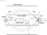
- the CMA consists of a coaxial cylindrical part consisting of an inner cylinder and an outer cylinder, a slit and a detector provided at the rear stage of the coaxial cylindrical part, and is an analyzer that utilizes the convergence effect of the cylindrically symmetrical electric field.
- the entrance of the inner cylinder into which electrons enter and the exit from which electrons exit is a cylindrical grid, which allows electrons to pass through without breaking the cylindrically symmetrical electric field.
- E pass is the CMA pass energy
- R in is the inner cylinder radius
- e is the elementary charge
- the absolute value of the voltage applied to the outer cylinder is approximately 0.75 times the converted accelerating voltage.
- the voltage applied to the inner cylinder is 0 times the converted acceleration voltage.
- the electron incident on the cylindrically symmetric electric field receives a force directed toward the central axis z and changes direction.
- the convergence point moves to the right when E k > E pass and to the left when E k ⁇ E pass , and electrons cannot pass through the slit when E k is shifted by the energy resolution.
- FIG. 24 shows the relationship between the incident angle ⁇ and the aperture aberration when the distance L between the origin on the sample and the point where the central orbit intersects the z-axis is 275 mm (When L is set to 275 mm, the length of the center trajectory from the origin to the slit position substantially matches the length of the center trajectory of the concentric hemispherical part shown in FIG. 21 ).
- K should be chosen to be 1.31 to limit the incident angle.
- K should be set to a value slightly larger than 1.31 (for example, about 1.33).
- the value of K can be easily changed by the voltage applied to the outer cylinder. Note, however, that as the value of K changes, so does the value of L, as described above. In other words, when the value of L changes, there is a problem that the optimal slit and detector positions change.
- the cylindrically symmetrical electric field used in CMA has a stronger convergence effect than the spherically symmetrical electric field used in CHA.
- the CMA has a third-order aperture aberration
- the CHA has a second-order aperture aberration.
- the CMA is expected to have a high energy resolution, but the CMA has not actually achieved the high energy resolution like that obtained with the CHA.
- the reason for not achieving is that two grid electrodes are used in the CMA, and the electrons are scattered by the grid at the entrance and exit of the cylindrically symmetric electric field, resulting in poor convergence.
- Typical spin polarization analyzers include Mott detectors and SPLEED detectors using spin-orbit interaction, and VLEED detectors using spin-exchange interaction. Also, in recent years, the two-dimensional spin analyzer using an Ir (001) single crystal substrate has been developed (Non-Patent Document 10).
- FIG. 25 is a schematic view of the VLEED detector (Non-Patent Document 11).
- This spin polarization analyzer is a detector that utilizes the fact that, when low-energy electrons are incident on a target magnetized by a coil, the intensity of the reflected electrons changes depending on whether the electron spin is parallel or antiparallel to the magnetization of the target. An iron thin film is used as the target.
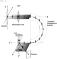
- FIG. 26 is a schematic view of the spin polarization analyzer that combines the CHA and the VLEED.
- z and z' are the optical axes between the sample and the concentric hemispherical part and between the concentric hemispherical part and the target, respectively.
- y, y' are axes in the direction connecting the center and the entrance or exit of the concentric hemispherical part, and
- x, x' are axes perpendicular to z, y and z', y', respectively. Since the CHA consists only of the electric field, the direction of the spin does not change even if the electron passes through the CHA.
- a coil is provided in the y' direction and the spin polarization in the y direction within the sample surface can be measured.
- the sample may be rotated by 90° in the in-plane direction, but the rotation of the sample causes even a slight shift in the measurement area. This can be a fatal problem in micro-area analysis.
- it is effective to provide the spin rotator that rotates the spin by 90° in a plane perpendicular to the lens axis in the input lens or in front of the spin analyzer.
- the spin in the in-plane direction of the sample can be rotated by 90° without rotating the sample.
- the spin polarization analyzer using the VLEED instead of the spin rotator, coils for magnetizing the target are provided in two directions, and by switching the magnetization direction, the spin polarization in the x direction and the y direction in the sample surface can be measured.
- none of the above methods can measure spin polarization in the z direction.
- An effective method for measuring the spin polarization in the z direction is to bend the electron trajectory by 90° with the electric field before the electron enters the target.
- FIG. 27 is a schematic view of the spin polarization analyzer for spin analysis in such a manner.
- the electron trajectory is bent by 90° in the z'y' plane, which makes it possible to measure the spin polarization normal to the sample surface (z direction).
- a 1/4 cylindrical electrostatic 90° deflector as shown in FIG. 27 is used.
- the spin rotators are disposed respectively between the input lens and the concentric hemispherical part, and the 90° deflector and the spin analyzer as in FIG. 27 .
- both of two spin rotators (SR1, SR2) are set to OFF.
- SR1 is set to OFF and SR2 is set to ON, the spin polarization in the x direction in the sample surface can be measured, and when both SR1 and SR2 are set to ON, the spin polarization in the y direction in the sample surface can be measured.
- a coil may be added in the x' direction instead of providing the second spin rotator SR2.
- Three-dimensional spin polarization can be measured by the above method.
- FIG. 28 is a schematic view of a spin polarization analyzer using a 90° spherical deflector.
- the 90° deflector or the 90° spherical deflector has a simple structure and is suitable for bending a parallel beam by 90°. However, these deflectors cannot converge an angularly spread beam emanating from a single point.
- FIG. 29 is a schematic cross-sectional view of an improved 90° deflector.
- an electron beam emitted from one point can be deflected by 90° within the deflection plane and converged.
- the beam cannot be converged simultaneously in two directions, i.e., the direction within the deflection plane and the direction perpendicular thereto.
- the 90° spherical deflector it is possible to narrow the spread beam by combining a lens at the exit as shown in FIG. 30 .
- beams cannot be converged in two directions at the same time.
- the 90° deflection analyzer shown in FIGS. 27 to 30 can be used for three-dimensional measurements of spin polarization, but instead of using such a deflection analyzer, a Wien filter-type spin rotator can be used for the three-dimensional measurements of spin polarization.
- the spins perpendicular to the sample surface can be rotated by 90° and tilted in the in-plane direction without changing the direction of the beam, and as shown in FIG. 31 , a multipole Wien filter allows three-dimensional manipulation of the spins.
- this method does not achieve two-dimensional convergence of a beam with an angular spread at the same time as the 90° spin rotation.
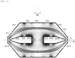
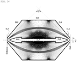
- FIG. 1(1) is a schematic view of Example 1 of the 90° electrostatic deflection convergence-type energy analyzer of the present invention.
- the 90° electrostatic deflection convergence-type energy analyzer 1 has five outer electrodes EL1, EL2, EL3, EL4, EL5 and three inner electrodes EL6, EL7, EL8 disposed along the shape of two rotation bodies formed inside and outside with a rotation axis 13 in common, and an electron incident hole 11 and an electron exit hole 12 are formed on respective rotation axis 13 of the electrodes at both ends of the outer electrode.
- the inner surface shape of the outer electrode has a tapered shape with a smaller diameter toward the incident hole 11 and the exit hole 12 except for the central electrode (EL3), and the outer surface shape of the inner electrode has a tapered shape with a smaller diameter toward the incident hole 11 and the exit hole 12 except for the center electrode (EL7).
- the energy analyzer 1 along the three-dimensional surface shape of the two rotation bodies obtained by rotating the lower bases of two isosceles trapezoids (20a, 20b) with different heights on the rotation axis 13, has five outer electrodes EL1, EL2, EL3, EL4, EL5 and three inner electrodes L6, EL7, EL8.
- a voltage for accelerating and decelerating electrons is applied to the outer electrode and the inner electrode in proportion to the energy of the incident electrons.
- one or a plurality of electrodes except for the inner electrodes at both ends have set thereto a voltage that is three times or more a converted acceleration voltage obtained by converting the energy of electrons into an acceleration voltage with reference to the potential of the outer electrode having the incident hole 11 formed therein.
- the voltage applied to each electrode is adjusted.
- the central trajectory is thus turned 90° by the electric field.
- the incident angle measured from the central orbit is ⁇
- the electron beam or light is irradiated through a hole (not shown) made in the inner electrode or the outer electrode.
- a slit for energy selection is disposed at the exit position, and a detector is disposed at the subsequent stage.
- a slit for energy selection is disposed at the exit position, and a detector is disposed at the subsequent stage.
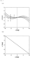
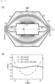
- FIG. 2(a) is a graph showing the aperture aberration of the 90° electrostatic deflection convergence-type energy analyzer of FIG. 1(1) .
- the length L of the analyzer is set to 275 mm (in this case, the length of the central trajectory approximately matches the length of the central trajectory of the concentric hemispherical part of the CHA shown in FIG. 21 ).
- A, B, C, and D shown in a graph of FIG. 2(a) are, respectively, the results of adjusting the voltage applied to each electrode (EL1 to EL8) so that the image blur due to the aperture aberration is reduced when the range of the incident angle ⁇ (acceptance cone angle) of the energy analyzer is set to ⁇ 2°, ⁇ 6°, ⁇ 8°, ⁇ 10°.
- the image blur due to aperture aberration is greatly reduced compared to the case of the CHA shown in FIG. 21 . Also in the CMA, as shown in FIG. 24 , by adjusting the applied voltage according to the acceptance cone angle, it is possible to minimize the image blur due to aperture aberration. However, in this case, the difficulty is that the convergence position changes.
- the applied voltage can be optimized without changing the convergence position.
- the image blur due to aperture aberration can be reduced to the same level as the CMA or less.
- the energy analyzer of the present invention unlike the CMA, does not use a grid electrode. It is desirable not to use the grid electrode in the energy analyzer with an imaging function, because the trajectory of electrons is disturbed when electrons pass through the grid electrode.
- FIG. 2(b) shows the relationship between the incident angle and the exit angle when the acceptance cone angle is ⁇ 10°.
- the energy analyzer of the present invention is suitable for angular distribution measurements.
- Table 2 shows voltage values when the electrode EL1 is set to the ground potential
- EL1 may be a potential V1 ( ⁇ 0) other than the ground potential.
- voltages obtained by adding V1 to the voltages shown in Table 2 are applied to the electrodes other than EL1.
- the electrodes EL1 and EL5 are set to the ground potential
- EL2, EL4, EL6 and EL8 are set to the same potential, and only the voltages of EL3 and EL7 are adjusted.
- EL3 is applied a voltage about 3 to 4 times the converted accelerating voltage
- EL7 is applied a voltage about 23 to 25 times the converted accelerating voltage.
- the voltages applied to EL3 and EL7 are higher by one or two orders of magnitude.
- the optimum voltage applied to each electrode varies depending on the shape and arrangement of the electrodes. As a result, a voltage approximately 0 to 10 times the converted acceleration voltage is applied to EL3, and a voltage approximately 10 to 50 times the converted acceleration voltage is applied to EL7.
- the voltage applied to EL7 may be 3 to 5 times or more and 10 times or less of the converted acceleration voltage.
- Voltage (V) @EL1 Voltage (V) @EL2 Voltage (V) @EL3 Voltage (V) @EL4 Voltage (V) @EL5 Voltage (V) @EL6 Voltage (V) @EL7 Voltage (V) @EL8 A 0 180 4480 180 0 180 24750 180 B 0 180 4350 180 0 180 24310 180 C 0 180 4240 180 0 180 23950 180 D 0 180 4110 180 0 180 23500 180
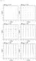
- FIGS. 3(a) to 3(d) show the results of calculating the energy dispersion in the 90° electrostatic deflection convergence-type energy analyzer of FIG. 1(1) .
- Energy resolution can be estimated from this dispersion.
- Table 3 below shows calculated contributions corresponding to the first term on the right side of the above equation (5), which indicates the energy resolution in the case of the CHA. This is an estimate of the energy resolution that is possible when the spot size of the illumination beam is brought close to zero.
- the 90° electrostatic deflection convergence-type energy analyzer has a smaller contribution corresponding to the second term on the right side of the above equation (5), and can achieve high energy resolution.
- [Table 3] ⁇ max ⁇ 2° ⁇ 3° ⁇ 4° ⁇ 5° ⁇ 6° ⁇ 8° ⁇ E / E [10 -2 ] 0.037 0.109 0.258 0.541 0.975 2.829
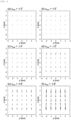
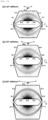
- FIGS. 4(a) to 4(f) show calculation results of the two-dimensional real-space image in the 90° electrostatic deflection convergence-type energy analyzer of FIG. 1(1) , as in FIG. 22 .
- the maximum value of the incident angle ⁇ is considered from ⁇ 2° to ⁇ 8°.
- the acceptance cone angle is set to about ⁇ 2° or less, a large aperture aberration occurs and a practical two-dimensional image cannot be obtained.
- FIG. 22 shows that the acceptance cone angle is set to about ⁇ 2° or less, a large aperture aberration occurs and a practical two-dimensional image cannot be obtained.
- the 90° electrostatic deflection convergence-type energy analyzer can obtain the practical two-dimensional image even if the acceptance cone angle is widened to about ⁇ 5° to ⁇ 6°. Also, at this acceptance cone angle, from a comparison of Tables 1 and 3, an energy resolution comparable to that of the CHA can be achieved.
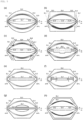
- FIGS. 5(a) to 5(h) show schematic views of examples of the 90° electrostatic deflection convergence-type energy analyzer of the present invention having the same effect, although the shape and arrangement of the electrodes are different with the energy analyzer shown in FIG. 1(1) .
- electrons enter from the incident hole provided at one end of the outer electrode and converge at the position of the exit hole provided at the other end.
- the shape of the electrode means the shape of the inner surface in the case of the outer electrode, and the shape of the outer surface in the case of the inner electrode.
- FIG. 5(a) shows an energy analyzer of the invention, in which a plurality of outer electrodes and a plurality of inner electrodes are disposed along the two rotation surfaces formed on the inside and the outside for a common rotation axis, and the outer and inner electrodes have toroidal surface shapes.
- the outer electrode and the inner electrode having toroidal surface shapes have diameters that decrease toward the incident hole and the exit hole, and the space formed between them narrows toward both ends.
- FIG. 5(b) shows a schematic view of an energy analyzer of the invention, in which a plurality of outer electrodes and a plurality of inner electrodes are disposed along the two rotation surfaces formed on the inside and the outside for a common rotation axis, and some of the outer electrodes are ring-shaped electrodes with round holes drilled in the plate, and the inner electrodes have a tapered shape with decreasing diameter towards the incident and exit holes.
- the hole diameter of the ring-shaped electrode near the incident hole and the exit hole is set small so that the space formed between the outer electrode and the inner electrode becomes narrower around the incident hole and the exit hole.
- FIG. 5(c) shows a schematic view of an energy analyzer of the invention, in which a plurality of outer electrodes and a plurality of inner electrodes are disposed along the two rotation surfaces formed on the inside and the outside for a common rotation axis, and some of the outer electrodes are ring-shaped electrodes with a tapered shape that decreases in diameter toward the incident and exit holes.
- the inner electrode has a tapered shape in which the diameter decreases toward the incident hole and the exit hole, and the ring-shaped electrode is set to have a small hole diameter near the incident hole and the exit hole.
- FIG. 5(d) shows a schematic view of an energy analyzer of the invention, in which a plurality of outer electrodes and a plurality of inner electrodes are disposed along the two rotation surfaces formed on the inside and the outside for a common rotation axis, and the inner electrode has a step shape extending to the vicinity of the incident and exit holes.
- the outer electrode has a tapered shape in which the diameter decreases toward the incident hole and the exit hole, and the space formed between the outer electrode and the inner electrode is narrowed around the incident hole and the exit hole.
- FIG. 5(e) shows a schematic view of an energy analyzer of the invention, in which a plurality of outer electrodes and a plurality of inner electrodes are disposed along the two rotation surfaces formed on the inside and the outside for a common rotation axis, and the inner electrode has a rod shape extending to the vicinity of the incident hole and the exit hole.
- the plurality of rod-shaped electrodes may have different outer diameters.
- FIG. 5(f) shows a schematic view of an energy analyzer of the invention, in which a plurality of outer electrodes and a plurality of inner electrodes are disposed along the two rotation surfaces formed on the inside and the outside for a common rotation axis, and the inner electrode has an axisymmetric shape with a diameter that widens at the ends.
- FIGS. 5(g) is an example of an energy analyzer of the present invention in which the number of inner electrodes is set to two and FIGS. 5(h) is an example of an energy analyzer of the present invention in which the number of outer electrodes is set to two.
- a plurality of outer electrodes and a plurality of inner electrodes are disposed along the two rotation surfaces formed on the inside and the outside for a common rotation axis, and the outer electrode is the same electrode as in FIG. 1(1)
- the inner electrode consists of a rod-shaped or cylindrical electrode extending to the vicinity of the incident hole and the exit hole, and a bead-shaped electrode passing through the rod-shaped or cylindrical electrode.
- FIG. 5(h) shows that the outer electrode consists of an axially symmetrical electrode extending to the incident hole and the exit hole and an axially symmetrical electrode disposed inside.
- the inner electrode has a tapered shape with a smaller diameter toward the incident hole and the exit hole.
- the convergence performance is degraded. Therefore, the acceptance cone angle is set small compared to other designs. If the acceptance cone angle can be even smaller, combining the inner electrode of FIG. 5(g) with the outer electrode of FIG. 5(h) , an energy analyzer of the present invention can be designed with a total of four electrodes, two inner electrodes and two outer electrodes. In the type of FIG.
- the convergence performance in order to improve the convergence performance, it is effective to optimize the shape by increasing the degree of freedom of the shape of the inner electrode, or to design by increasing the number of bead electrodes. Also, in the type of FIG. 5(h) , the convergence performance can be improved by a design in which the number of outer electrodes is increased.
- FIGS. 5(a) to 5(h) voltages for accelerating and decelerating electrons are applied to the outer and inner electrodes in proportion to the energy of incident electrons, as in the case of FIG. 1(1) .
- a voltage that is 3 to 5 times or more as high as the converted acceleration voltage obtained by converting electron energy into an acceleration voltage is set on one or more of the inner electrodes excluding the electrodes at both ends of the inner electrode, with reference to the potential of the outer electrode in which the incident hole is formed.
- the number of electrodes is not limited to those shown in FIG. 1(1) and FIG. 5 .
- the number of inner electrodes and outer electrodes may be two or more, but considering both performance and cost, it is preferable to provide about 3 to 5 inner electrodes and about 3 to 7 outer electrodes.
- the inner electrode and the outer electrode have a shape and arrangement in which the space formed between them narrows around the incident hole and the exit hole, as shown in FIG. 1(1) and FIG. 5 . As a result, the electric field applied to the incident hole and the exit hole can be kept small.
- the inner electrode and the outer electrode are desirably symmetrical with respect to a plane perpendicularly intersecting the straight line connecting the incident hole and the exit hole at the midpoint of the straight line.
- the actual design does not necessarily have to be plane symmetrical, and a non-plane symmetrical shape is also possible depending on the overall design of the analyzer.
- electrons in the central orbit enter at the incident angle of 45° and exit at the exit angle of 45°, but the incident angle and the exit angle of the central orbit are not limited to this.
- the inner electrode and the outer electrode are preferably shaped asymmetrically with respect to a plane perpendicularly intersecting the straight line connecting the incident hole and the exit hole at the midpoint of the straight line.
- FIG. 5 shows various types of electrode shapes. These shape types can be freely combined to design various forms of electrostatic deflection convergence-type energy analyzers, not limited to those shown in FIG. 5 .
- the combination of shape types can be freely changed not only for the outer electrode and the inner electrode, but also for the incident hole side and the exit hole side.
- FIG. 6(a) shows a schematic view of one embodiment of the imaging-type electron spectrometer of the present invention, in which an input lens is disposed in the front stage of the 90° electrostatic deflection convergence-type energy analyzer of FIG. 1(1) , and the projection lens is disposed in the rear stage.
- High energy resolution can be achieved in a wide energy range by decelerating the electrons emitted from the sample by the input lens and then introducing them into the energy analyzer.
- the 90° electrostatic deflection convergence-type energy analyzer can be expected to be very effective when combined with the input lens with a wide acceptance cone angle.
- the incident angle to the concentric hemispherical part must be about ⁇ 2° or less.
- magnification becomes very high. Even if the input lens converges with the same energy as at the time of incidence (without deceleration), if electrons with the opening angle of ⁇ 50° or ⁇ 90° are converged with the opening angle of ⁇ 2°, the magnification becomes about 25 or 45 times. When decelerating, the magnification is even higher.
- the magnification will be about 100 to 200 times according to the conservation of brightness.
- inserting a small aperture or slit at the incident and exit sides of the energy analyzer, as shown in FIG. 6(a) most electrons will not be able to pass through the aperture or slit, resulting in a significant loss of sensitivity.
- the 90° electrostatic deflection convergence-type energy analyzer of the present invention is therefore used instead of the CHA, the incident angle to the energy analysis section can be widened by about 3 times, and compared with the case of using the CHA, the sensitivity can be increased by about 9 times.
- FIG. 6(b) has the same basic configuration as the device in FIG. 6(a) , but the structure of the energy analyzer is slightly different.
- the energy analyzer is constructed as a 180° rotation body instead of a 360° rotation body to save space.
- FIG. 7 shows a cross-sectional view of the energy analyzers of FIGS. 6(a) and 6(b) taken perpendicularly to the paper.
- the inner electrode is fixed by a fixed leg.
- the fixed leg is disposed where the effect on the electric field is as small as possible, and the electrodes EL6 and EL8 are fixed to the electrodes EL2 and EL4, respectively, by the fixed legs.
- a compensating electrode as shown in FIG. 7B is provided to compensate the electric field at the cut surface. Further space saving can be achieved by using an energy analyzer with a rotation angle of less than 180° instead of using the 180° rotation energy analyzer. In this case, it is desirable to set the rotation angle between 90° and 180°. Also, in the case of the energy analyzer with the rotation angle of less than 180°, the compensating electrode for compensating the electric field at the cut surface is provided as in FIG. 7(b) .
- FIG. 8 shows an embodiment of the reflection imaging-type electron spectrometer of the present invention.
- the reflection imaging-type electron spectrometer of this embodiment it is characterized in that the electrons deflected by 90° and converged by the 90° electrostatic deflection convergence-type energy analyzer of Example 1 are reflected by the single crystal mirror, and again deflected by 90° and converged. Electrons emitted from the sample are converged by the input lens and enter the energy analyzer through an aperture inclined at 45°. Incident electrons are deflected by 90° and converged, reflected by the single crystal mirror, returned to the position of the incident aperture by the 90° deflection convergence, and emitted from there in a direction perpendicular to the direction of incidence. The emitted electrons are imaged by the projection lens as the two-dimensional real-space image or emission angle distribution, and are applied to the detector.
- the entrance aperture also serves as an exit aperture that selects energy, and the energy resolution and sensitivity largely depend on the size of this aperture. Therefore, in order to adjust the energy resolution and sensitivity according to the measurement, the aperture section preferably has a plurality of apertures with different sizes, and it is desirable to have a mechanism for switching between them, or a mechanism such as an iris whose size can be freely changed.
- the energy analyzer in the reflection imaging-type electron spectrometer shown in FIG. 8 has twice the energy dispersion compared to the energy analyzer shown in FIG. 6 , higher energy resolution can be expected.
- noise may increase due to, for example, inelastic scattering by a single crystal mirror disposed in the exit hole of the energy analyzer, and the SN (Signal to Noise ratio) may decrease. Therefore, in order to reduce noise, it is effective to perform energy selection in two stages (two convergence positions).
- the selection by the above aperture is the second stage, and the first stage uses the single crystal mirror for energy selection as shown in FIG. 8 .
- the part corresponding to the aperture is a single crystal, and other parts are covered with electron absorbing materials.
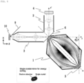
- FIG. 9 shows an embodiment of the spin vector distribution imaging apparatus of the present invention using the 90° electrostatic deflection convergence-type energy analyzer of FIG. 1(1) .
- a two-dimensional spin filter 8 is provided as shown in the drawing in order to measure the two-dimensional real-space image or emission angle distribution with spin resolution.
- An electrostatic lens 19 is provided in front of the two-dimensional spin filter 8 so that the electrons enter the two-dimensional spin filter 8 at an appropriate energy and angle, and these are adjusted.
- the electrons reflected by the two-dimensional spin filter 8 are projected onto the first detector 4a by the first projection lens 3a.
- the two-dimensional spin filter 8 can be retracted from the optical axis. In the retracted state, the second projection lens 3b and the second detector 4b are used to obtain a normal (spin-integrated) two-dimensional real-space image or two-dimensional emission angle distribution.
- the spin rotators 7a (SR1) and 7b (SR2) provided on the front and rear optical axes of the 90° deflection energy analyzer 1 are used for three-dimensional spin resolution within and normal to the sample surface.
- the SR1 and SR2 are set to rotate the spin by 90° in the surface normal to the optical axis (hereinafter referred to as "ON") or not (hereinafter referred to as "OFF").
- ON the surface normal to the optical axis
- OFF not
- the two-dimensional spin filter 8, the first projection lens 3a, and the first detector 4a may be rotated 90° in normal to the paper surface about the intersection point of the z'-axis and the z"-axis.
- the spin polarization in normal to the sample surface can be measured.
- both the SR1 and SR2 should be turned ON, and to measure the spin polarization in the y direction within the sample surface, only the SR2 should be turned ON.
- the spin vector distribution imaging apparatus with the spin rotator is shown in FIG. 9 and the following examples, the spin rotator is not necessarily required. Instead of providing the spin rotator, it is also possible to determine the direction of spins to be detected by rotating the sample and/or rotating the spin analyzer consisting of the two-dimensional spin filter, the projection lens and the detector. Also, although FIG. 9 shows the spin vector distribution imaging apparatus using the 360° rotation body type energy analyzer, a spin vector distribution imaging apparatus using an energy analyzer with a rotation angle of 180° or less can be also possible.
- FIG. 10 shows a schematic view of a simplified version of a spin vector distribution imaging apparatus using the reflection imaging-type electron spectrometer shown in FIG. 8 .
- the two-dimensional spin filter 8 such as Au/Ir (001) is used instead of the single crystal mirror. This provides a spin-analyzed two-dimensional real-space image or emission angle distribution at the detector.
- the input lens 2 may or may not have the spin rotator 7, like the spin vector distribution imaging apparatus shown in FIG. 9 . With the spin rotator, it becomes possible to measure the spin polarization in two directions within the sample surface.
- the spin polarization in the in-plane y direction (normal to the paper surface) of the sample 10 can be measured, and when the spin rotator 7 is turned on, the spin polarization in the in-plane x direction of the sample can be measured. Also, as described above, the spin polarization in two in-plane directions of the sample 10 can be measured by rotating the sample 10 instead of providing the spin rotator.
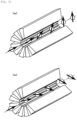
- FIG. 11 is a schematic view of one embodiment of a switching-type electrostatic deflection convergence-type energy analyzer of the present invention.
- the switching-type electrostatic deflection convergence-type energy analyzer shown in Fig. 11 has seven outer electrodes EL1, EL2, ..., EL7 and six inner electrodes EL8, EL9, ..., EL13, in which the outer electrode is axially symmetrical in inner surface shape, and the inner electrode is axially symmetrical in outer surface shape, and they are disposed coaxially.
- the entrance-side electrodes (EL1, EL2, EL8) have a tapered shape with a diameter narrowing toward the entrance
- the exit-side electrodes (EL6, EL7, EL13) have a tapered shape with a diameter narrowing toward the exit.
- the greatest feature of the switching-type electrostatic deflection convergence-type energy analyzer of FIG. 11 is that the inner electrode is separated into two regions, as the effect, electrons can pass through the space created between the left and right inner electrodes.
- the electron trajectories and equipotential lines shown in FIG. 11 are the results for the 90° deflection.
- FIGS. 12(a) and 12(b) show the results of switching the deflection by changing the voltage conditions in the switching-type electrostatic deflection convergence-type energy analyzer of FIG. 11 .
- the electrons pass through the electric field formed between the left and right inner electrodes.
- the energy dispersion in the case of Fig. 12(a) , is almost the same as in the case of Fig. 11 , but in the case of FIG. 12(b) , the cancellation effect results in a significant reduction compared to the case of FIG. 12(a) .
- the setting of FIG. 12(a) can be suitably used for energy analysis
- the setting of FIG. 12(b) can be suitably used for PEEM (photoemission electron microscope) measurement with suppressed chromatic aberration.
- FIG. 13 shows a schematic view of a spin vector distribution imaging apparatus using the switching-type electrostatic deflection convergence-type energy analyzer shown in FIGS. 11 and 12 .
- Three measurement modes are shown.
- FIG. 13(a) is a spin-resolved mode
- FIG. 13(b) is a spin-integrated mode
- FIG. 13(c) is a PEEM (photoemission electron microscope) mode.
- a deflection switching energy analyzer is set to the condition of 90° deflection.
- the electrostatic lens 19, the second spin rotator 7b (SR2), the two-dimensional spin filter 8, the first projection lens 3a (provided in normal to the paper surface), and the first detector 4a, for electrons deflected by 90°, are provided.
- the three-dimensional spin polarization can be measured by the same principle as the three-dimensional spin polarization analyzer of FIG. 9 .
- both the second spin rotator 7b (SR2) and the first spin rotator 7a (SR1) are set to OFF, the perpendicular spin polarization of the sample 10 can be measured.
- the second projection lens 3b and the second detector 4b provided for the S-shaped-trajectory electrons can measure a normal two-dimensional real-space image or the two-dimensional emission angle distribution without spin resolution.
- the measurement of the two-dimensional real-space image is performed using the sharp photoelectron spectrum peak of core excitation.
- most of the photoelectrons emitted by irradiation with vacuum ultraviolet rays or X-rays are secondary electrons.
- the secondary electrons are electrons that have lost energy in various processes prior to emission and have a wide range of energies.
- the PEEM mode of FIG. 13(c) is a mode for measuring such a PEEM image.
- the setup of FIG. 12(b) is used in which the energy dispersion is cancelled. This makes it possible to obtain clear PEEM images with suppressed chromatic aberration.
- the apparatus of FIG. 13 is characterized by having the function of this PEEM measurement (compared to the apparatus of FIG. 9 ) and being able to switch the measurement mode only by the voltage applied to each element.
- the electrostatic energy analyzer of this example is composed of a combination of two or more electron optical systems.
- each electron optical system to be combined may be an electrostatic convergence mirror, an electrostatic deflector, or an electrostatic lens.
- a and B schematically represent two electron optical systems used for the combination.
- the A has a deflection angle ⁇ 1 and the B has a deflection angle ⁇ 2 .
- the center trajectory is not the center axis of the lens, but a trajectory that enters at a constant angle from the center axis and exits at a constant angle, and the deflection angle at this time is ⁇ 1 or ⁇ 2 . It is assumed that central orbital electrons are incident or emitted perpendicularly to both end faces of the A and B, respectively.
- Both end faces of the A and B are disposed perpendicular to the xy plane, and the right end face of A and the left end face of B are disposed face to face.
- FIG. 16(b) shows the condition of the 90° deflection for some ⁇ 1 when ⁇ 2 ⁇ ⁇ 1 .
- FIGS. 17(a) and 17(b) are examples of a 45° electrostatic deflection convergence-type energy analyzer and a 60° electrostatic deflection convergence-type energy analyzer, respectively.
- the central trajectory is a trajectory at an angle of 22.5° from the central axis in the case of the 45° electrostatic deflection convergence-type energy analyzer, and at an angle of 30° from the central axis in the case of the 60° electrostatic deflection convergence-type energy analyzer.
- FIGS. 17(a) and (b) show trajectories with an incident angle range of ⁇ 8° measured from the central trajectory. The convergence of these trajectories is lower than that of the 90° electrostatic deflection convergence-type energy analyzer shown in FIG. 1(1) , but high convergence can be obtained by limiting the incident angle to about ⁇ 5°.
- FIG. 17(a) shows a 90° electrostatic deflection convergence-type energy analyzer with this combination.
- FIG. 18(b) shows a 90° electrostatic deflection convergence-type energy analyzer with this combination.
- FIGS. 19(a), 19(b), and 19(c) show schematic views of examples of the 120° electrostatic deflection convergence-type energy analyzer, the 135°electrostatic deflection convergence-type energy analyzer, and the 150° electrostatic deflection convergence-type energy analyzer, respectively.
- the central trajectories are trajectories incident at angles of 60°, 67.5° and 75° from the central axis, respectively.
- FIGS. 19(a), 19(b), and 19(c) show trajectories with an incident angle range of ⁇ 8° measured from the central trajectory. These trajectories have improved convergence compared to the trajectories of FIGS. 17(a) and 17(b) .
- the energy analyzer with a deflection angle of more than 150° and 180° or less with the same electrode configuration as in FIG. 19 .
- the deflection angle is about 160° or more, the convergence performance drops significantly.
- the 90° deflection can be achieved using an analyzer with a large deflection angle as in FIGS. 19(a) and 19(b) .
- the energy analyzer with the rotation angle of 180° or less is used instead of the 360° rotation type (see FIG. 7 ) as shown in FIG. 17 due to geometric constraints.
- the energy analyzer with a small deflection angle and the energy analyzer with a large deflection angle each have advantages and disadvantages.
- the smaller the deflection angle the smaller the energy dispersion and the lower the energy resolution.
- the voltage applied to at least one of the inner electrodes may be about 2 to 5 kV or more and about 10 kV or less with respect to 1000 eV.
- electrostatic deflection convergence-type energy analyzer with a specific deflection angle is shown as an example, the electrostatic deflection convergence-type energy analyzer of the present invention can also be provided as the energy analyzer with any deflection angle from 45° to 180° by a similar design.
- the ratio of the outer diameter to the length L of the inner electrode is approximately 0.12
- the ratio of the inner diameter to the length L of the outer electrode is approximately 0.64.
- the ratio of the outer diameter to the length L of the inner electrode is approximately 0.27, and the ratio of the inner diameter to the length L of the outer electrode is approximately 0.76.
- image blur due to aperture aberration is increased by about 13 times as compared with the configuration of the electrostatic deflection convergence-type energy analyzer shown in FIG. 1 .
- the voltage applied to the EL7 is lowered to about ten times the converted acceleration voltage, the deterioration of the convergence performance becomes remarkable.
- this deterioration of the convergence performance can be greatly reduced by appropriately shaping the inner electrode.
- FIG. 33(a) shows an example of an appropriate shape for the inner electrode in the electrostatic deflection convergence-type energy analyzer of the present invention.
- the EL7 is set to a voltage 10 times the converted acceleration voltage.
- the EL6 and EL8 have a stepped shape characterized by two outer diameters D1 and D2 (D1 ⁇ D2), unlike the electrostatic deflection convergence-type energy analyzers shown in FIGS. 1 and 32(a) .
- the ratio of D1 to length L is 0.11
- the ratio of D2 to length L is 0.24.
- the ratio of the inner diameter of the outer electrode to the length L is approximately 0.76.
- the convergence performance is inferior to that of the electrostatic deflection convergence-type energy analyzer shown in FIG. 1 , as shown in FIG. 33(b) .
- the performance can be greatly improved as compared with the electrostatic deflection convergence-type energy analyzer shown in FIG. 32(a) .
- the EL6 and EL8 have tapered parts that decrease in diameter toward the entrance or exit, as in the case of the electrostatic deflection convergence-type energy analyzers shown in FIGS. 1 and 32(a) .
- a design without this tapered part is also effective, and the simplest shape may be a coaxial two-stage cylindrical shape characterized only by two outer diameters D1 and D2 and two lengths in the z-axis direction.
- FIG. 34 shows an example of the electrostatic deflection convergence-type energy analyzer of the present invention in which a lower voltage is applied to the inner electrode EL7.
- the inner electrodes EL6 and EL8 have the stepped shape with the tapered part on the entrance or exit side.
- FIG. 34 shows an example of the electrostatic deflection convergence-type energy analyzer of the present invention in which a lower voltage is applied to the inner electrode EL7.
- the design without the tapered part is also useful, and may be a coaxial two-step cylindrical shape characterized by only two outer diameters D1, D2 and two lengths along the z-axis.
- the outer surface of the EL7 has a cylindrical shape with the outer diameter larger than D1 and D2.
- the inner electrode has a coaxial three-stage cylindrical shape as a whole, except for the tapered part.
- FIGS. 34(a), (b), and (c) respectively show the results of adjusting the three outer diameters, the length of each part, and the applied voltage so that the aperture aberration is minimized.
- the ratio of the inner diameter to the length L of the outer electrode is approximately 0.76 in the case of the electrostatic deflection convergence-type energy analyzer shown in FIG. 34(a) , and is approximately 0.87 in the case of the electrostatic deflection convergence-type energy analyzer shown in FIGS. 34(b) and 34(c) .
- the aperture aberration for the electrostatic deflection convergence-type energy analyzer shown in FIGS. 34(a), (b), and (c) is shown in FIG. 35 , with the aperture aberration in the case of the electrostatic deflection convergence-type energy analyzer shown in FIGS. 1 and 33(a) .
- the point to be noted here is that the aperture aberration increases as the voltage applied to the EL7 is lowered. Therefore, for the purpose of reducing aperture aberration, it is desirable to set the voltage applied to the EL7 as high as possible.
- the aperture aberration abruptly increases when the voltage applied to the EL7 is lowered from 2 times to 1.5 times the converted acceleration voltage. Therefore, it is desirable to set the voltage applied to the EL7 to about twice or more the converted acceleration voltage.
- the aperture aberration can be further reduced by setting the voltage applied to the EL 7 higher than in the case of the electrostatic deflection convergence-type energy analyzer shown in FIG. 1 .
- the voltage applied to the EL7 cannot be set as high as desired, and is subject to restrictions in the design and manufacture of the inner diameter electrode.
- FIG. 36 shows an example of the electrostatic deflection convergence-type energy analyzer of the present invention when the voltage applied to the EL7 is set to 50 times the converted acceleration voltage.
- the outer diameter of the EL7 is smaller than the outer diameters of the EL6 and EL8.
- the limit of the voltage applied to the EL7 is about 50 times, and if it is attempted to be increased beyond this, the outside diameter of the EL7 becomes too small, which causes the problem of difficulty in wiring and insulation.
- the aperture aberration must be made sufficiently small.
- Table 8 summarizes the applied voltages in the case of electrostatic deflection convergence-type energy analyzers shown in FIGS. 32(a) , 33(a) , 34(a), 34(b), 34(c) and 36 . According to Table 8, it can be seen that methods of applying voltages to the EL1 to EL8 changes starting with the electrostatic deflection convergence-type energy analyzer shown in FIG. 34(b) .
- the voltage applied to the EL7 is about twice or more the converted acceleration voltage, 0 or positive voltage is applied to the other electrodes, and when the voltage applied to the EL7 is about twice or less the converted acceleration voltage, 0 or negative voltage is applied to the other electrodes.
- the outer electrodes EL1 to EL5 are all set to the same potential (0 V), so they can be also collectively designed as one electrode. Also, in the case of the electrostatic deflection convergence-type energy analyzer shown in FIG. 34(a) , the outer electrodes can also be designed as a total of three electrodes, since (adjacent) EL1, EL2 and EL4, EL5 are at the same potential (0 V). Thus, the number of outer electrodes is not limited to five, EL1 to EL5 shown in the example, but may be three or one, and may be two, four or six or more. Also, the number of inner electrodes is not limited to the three EL6 to EL8 shown in the example, and may be four or more.
- the shape and arrangement of the electrodes various changes are possible as long as they are set so as to form an electric field similar to the electric field shown in the example.
- the characteristics of the electric field of the electrostatic deflection convergence-type energy analyzer of the present invention will be described.
- the electrostatic deflection convergence-type energy analyzer of the present invention is fundamentally different from the electric fields used in the CMA and CHA.
- the present invention is useful for energy analyzers, photoelectron spectrometers, and spin polarization analyzers.
Landscapes
- Chemical & Material Sciences (AREA)
- Analytical Chemistry (AREA)
- Physics & Mathematics (AREA)
- Health & Medical Sciences (AREA)
- Life Sciences & Earth Sciences (AREA)
- Biochemistry (AREA)
- General Health & Medical Sciences (AREA)
- General Physics & Mathematics (AREA)
- Immunology (AREA)
- Pathology (AREA)
- Analysing Materials By The Use Of Radiation (AREA)
Applications Claiming Priority (2)
| Application Number | Priority Date | Filing Date | Title |
|---|---|---|---|
| JP2020118687 | 2020-07-09 | ||
| PCT/JP2021/026052 WO2022009995A1 (fr) | 2020-07-09 | 2021-07-09 | Analyseur d'énergie de type à convergence de déviation électrostatique, dispositif de spectroscopie d'électrons de type à imagerie, dispositif de spectroscopie d'électrons de type à imagerie réfléchissante et dispositif d'imagerie de distribution de vecteur de spin |
Publications (2)
| Publication Number | Publication Date |
|---|---|
| EP4170694A1 true EP4170694A1 (fr) | 2023-04-26 |
| EP4170694A4 EP4170694A4 (fr) | 2024-07-10 |
Family
ID=79552580
Family Applications (1)
| Application Number | Title | Priority Date | Filing Date |
|---|---|---|---|
| EP21836935.3A Pending EP4170694A4 (fr) | 2020-07-09 | 2021-07-09 | Analyseur d'énergie de type à convergence de déviation électrostatique, dispositif de spectroscopie d'électrons de type à imagerie, dispositif de spectroscopie d'électrons de type à imagerie réfléchissante et dispositif d'imagerie de distribution de vecteur de spin |
Country Status (5)
| Country | Link |
|---|---|
| US (1) | US20240047190A1 (fr) |
| EP (1) | EP4170694A4 (fr) |
| JP (1) | JP7607953B2 (fr) |
| CN (1) | CN115803844B (fr) |
| WO (1) | WO2022009995A1 (fr) |
Families Citing this family (1)
| Publication number | Priority date | Publication date | Assignee | Title |
|---|---|---|---|---|
| CN122117515B (zh) * | 2026-04-28 | 2026-07-17 | 华东师范大学 | 一种超低能单色化电子束产生与传输装置 |
Family Cites Families (23)
| Publication number | Priority date | Publication date | Assignee | Title |
|---|---|---|---|---|
| GB1327572A (en) * | 1971-03-23 | 1973-08-22 | Ass Elect Ind | Apparatus for use in charged particle spectroscopy |
| AT376044B (de) * | 1978-03-07 | 1984-10-10 | Oesterr Forsch Seibersdorf | Einrichtung zur fokussierung und zur analyse eines geladenen korpuskularstrahls |
| RU1826089C (ru) * | 1991-02-13 | 1993-07-07 | Научно-исследовательский технологический институт | Электростатический анализатор энергий зар женных частиц |
| JP3665032B2 (ja) * | 2002-02-27 | 2005-06-29 | 独立行政法人科学技術振興機構 | 高分解能電子エネルギー分析器 |
| DE10252129A1 (de) * | 2002-11-04 | 2004-05-27 | Omicron Nano Technology Gmbh | Energiefilter für elektrisch geladene Teilchen und Verwendung des Energiefilters |
| JP4133883B2 (ja) * | 2003-12-04 | 2008-08-13 | 日新イオン機器株式会社 | イオンビーム装置 |
| WO2006008840A1 (fr) | 2004-07-15 | 2006-01-26 | National University Corporation NARA Institute of Science and Technology | Lentille électrostatique de correction d’aberration sphérique, dispositif d’entrée, dispositif spectroscopique électronique, microscope photoélectronique et système de mesure |
| JP4777006B2 (ja) * | 2004-08-10 | 2011-09-21 | 富士通株式会社 | 3次元微細領域元素分析方法 |
| US7439520B2 (en) * | 2005-01-24 | 2008-10-21 | Applied Biosystems Inc. | Ion optics systems |
| EP2058834B1 (fr) | 2006-07-26 | 2015-12-09 | National University Corporation Nara Institute of Science and Technology | Lentille à décélération à correction d'aberration sphérique, système de lentilles à correction d'aberration sphérique, dispositif de spectroscopie électronique, et microscope à photoélectrons |
| DE102007024353B4 (de) * | 2007-05-24 | 2009-04-16 | Ceos Corrected Electron Optical Systems Gmbh | Monochromator und Strahlquelle mit Monochromator |
| GB0720901D0 (en) * | 2007-10-24 | 2007-12-05 | Shimadzu Res Lab Europe Ltd | Charged particle energy analysers |
| GB0801663D0 (en) * | 2008-01-30 | 2008-03-05 | Krizek Jiri G F | Electromagnetic imaging analyzer |
| US8013298B2 (en) * | 2008-07-14 | 2011-09-06 | National University Of Singapore | Electrostatic electron spectrometry apparatus |
| US8129695B2 (en) * | 2009-12-28 | 2012-03-06 | Varian Semiconductor Equipment Associates, Inc. | System and method for controlling deflection of a charged particle beam within a graded electrostatic lens |
| KR101820190B1 (ko) | 2010-11-17 | 2018-01-18 | 스펙스 서피스 나노 아날리시스 게엠베하 | 입자 빔에서 주된 스핀 벡터의 벡터 성분을 측정하기 위한 스핀 검출기 구조 |
| JP5826529B2 (ja) * | 2011-06-17 | 2015-12-02 | サンユー電子株式会社 | スピン回転装置 |
| GB201118279D0 (en) * | 2011-10-21 | 2011-12-07 | Shimadzu Corp | Mass analyser, mass spectrometer and associated methods |
| DE102013005173C5 (de) * | 2013-03-25 | 2019-04-04 | Johannes Gutenberg-Universität Mainz | Messvorrichtung und Verfahren zur Erfassung einer Impulsverteilung geladener Teilchen |
| RU136236U1 (ru) * | 2013-07-24 | 2013-12-27 | Федеральное государственное бюджетное образовательное учреждение высшего профессионального образования "Рязанский государственный радиотехнический университет" | Энерго-масс-анализатор ионных потоков |
| JP6576751B2 (ja) * | 2015-09-07 | 2019-09-18 | 日本電子株式会社 | 分析方法およびx線光電子分光装置 |
| WO2019216348A1 (fr) * | 2018-05-09 | 2019-11-14 | 国立大学法人奈良先端科学技術大学院大学 | Lentille électrostatique de correction d'aberration sphérique à rapport de réduction variable, analyseur d'énergie à grand angle et spectromètre d'électrons bidimensionnel |
| JP7505794B2 (ja) | 2019-12-17 | 2024-06-25 | 大学共同利用機関法人自然科学研究機構 | 球面収差調整カソードレンズ、球面収差補正静電型レンズ、電子分光装置、及び光電子顕微鏡 |
-
2021
- 2021-07-09 US US18/015,057 patent/US20240047190A1/en active Pending
- 2021-07-09 WO PCT/JP2021/026052 patent/WO2022009995A1/fr not_active Ceased
- 2021-07-09 CN CN202180049046.0A patent/CN115803844B/zh active Active
- 2021-07-09 JP JP2022535410A patent/JP7607953B2/ja active Active
- 2021-07-09 EP EP21836935.3A patent/EP4170694A4/fr active Pending
Also Published As
| Publication number | Publication date |
|---|---|
| JPWO2022009995A1 (fr) | 2022-01-13 |
| EP4170694A4 (fr) | 2024-07-10 |
| CN115803844A (zh) | 2023-03-14 |
| JP7607953B2 (ja) | 2025-01-06 |
| WO2022009995A1 (fr) | 2022-01-13 |
| US20240047190A1 (en) | 2024-02-08 |
| CN115803844B (zh) | 2026-05-08 |
Similar Documents
| Publication | Publication Date | Title |
|---|---|---|
| Fink et al. | SMART: A planned ultrahigh-resolution spectromicroscope for BESSY II | |
| CN112305002B (zh) | 光谱学和成像系统 | |
| EP1305816B1 (fr) | Collecte d'electrons secondaires a travers l'objectif d'un microscope electronique a balayage | |
| Rose | Prospects for realizing a sub-Å sub-eV resolution EFTEM | |
| EP1432006B1 (fr) | Filtre d'énergie et microscope électronique | |
| Liebl | Design of a combined ion and electron microprobe apparatus | |
| US11791148B2 (en) | Variable reduction ratio spherical aberration correction electrostatic lens, wide angle energy analyzer, and two-dimensional electron spectrometer | |
| US7655923B2 (en) | Spherical aberration corrected electrostatic lens, input lens, electron spectrometer, photoemission electron microscope and measuring system | |
| US7250599B2 (en) | Energy filter image generator for electrically charged particles and the use thereof | |
| US8373137B2 (en) | High resolution energy-selecting electron beam apparatus | |
| US20240047190A1 (en) | Electrostatic deflection convergence-type energy analyzer, imaging-type electron spectroscopic device, reflecting imaging-type electron spectroscopic device, and spin vector distribution imaging device | |
| US7569816B1 (en) | Electron spectrometer | |
| JP7505794B2 (ja) | 球面収差調整カソードレンズ、球面収差補正静電型レンズ、電子分光装置、及び光電子顕微鏡 | |
| JP4781211B2 (ja) | 電子線装置及びこれを用いたパターン評価方法 | |
| Martı́nez et al. | Design of Wien filters with high resolution | |
| Matsuda et al. | Compact 2D electron analyzer CoDELMA: Simultaneous wide reciprocal and real space analysis using wide-angle deceleration lens, CMA and projection lens | |
| Tsuno | Simulation of a Wien filter as beam separator in a low energy electron microscope | |
| US11094498B2 (en) | Monochromator and charged particle beam system | |
| DE102020104151B3 (de) | Abbildungsvorrichtung für Elektronen und ein Abbildungsverfahren zur Reduktion des Untergrundsignals in abbildenden elektronenoptischen Geräten | |
| Ogawa et al. | A new monochromator with multiple offset cylindrical lenses | |
| Kienle et al. | An off-axis multi-channel analyzer for secondary electrons | |
| Belov et al. | Two-stage systems with intermediate beam retarding for energy and spatial analysis of photoelectrons | |
| Belov et al. | Design of a versatile energy analyzer for photoelectron spectroscopy studies at synchrotron radiation sources | |
| JP2006278069A (ja) | ウィーンフィルタ型エネルギーアナライザ及び放出電子顕微鏡 | |
| EP1739714A1 (fr) | Système d'imagerie pour courants élevés |
Legal Events
| Date | Code | Title | Description |
|---|---|---|---|
| STAA | Information on the status of an ep patent application or granted ep patent |
Free format text: STATUS: THE INTERNATIONAL PUBLICATION HAS BEEN MADE |
|
| PUAI | Public reference made under article 153(3) epc to a published international application that has entered the european phase |
Free format text: ORIGINAL CODE: 0009012 |
|
| STAA | Information on the status of an ep patent application or granted ep patent |
Free format text: STATUS: REQUEST FOR EXAMINATION WAS MADE |
|
| 17P | Request for examination filed |
Effective date: 20230119 |
|
| AK | Designated contracting states |
Kind code of ref document: A1 Designated state(s): AL AT BE BG CH CY CZ DE DK EE ES FI FR GB GR HR HU IE IS IT LI LT LU LV MC MK MT NL NO PL PT RO RS SE SI SK SM TR |
|
| DAV | Request for validation of the european patent (deleted) | ||
| DAX | Request for extension of the european patent (deleted) | ||
| REG | Reference to a national code |
Ref country code: DE Ref legal event code: R079 Free format text: PREVIOUS MAIN CLASS: H01J0037050000 Ipc: H01J0049480000 |
|
| A4 | Supplementary search report drawn up and despatched |
Effective date: 20240612 |
|
| RIC1 | Information provided on ipc code assigned before grant |
Ipc: H01J 37/252 20060101ALI20240606BHEP Ipc: H01J 37/05 20060101ALI20240606BHEP Ipc: G01N 23/227 20180101ALI20240606BHEP Ipc: H01J 49/48 20060101AFI20240606BHEP |