EP4170700A1 - Indiumphosphidsubstrat - Google Patents
Indiumphosphidsubstrat Download PDFInfo
- Publication number
- EP4170700A1 EP4170700A1 EP22725154.3A EP22725154A EP4170700A1 EP 4170700 A1 EP4170700 A1 EP 4170700A1 EP 22725154 A EP22725154 A EP 22725154A EP 4170700 A1 EP4170700 A1 EP 4170700A1
- Authority
- EP
- European Patent Office
- Prior art keywords
- wafer
- main surface
- surface side
- less
- indium phosphide
- Prior art date
- Legal status (The legal status is an assumption and is not a legal conclusion. Google has not performed a legal analysis and makes no representation as to the accuracy of the status listed.)
- Pending
Links
Images


Classifications
-
- C—CHEMISTRY; METALLURGY
- C30—CRYSTAL GROWTH
- C30B—SINGLE-CRYSTAL GROWTH; UNIDIRECTIONAL SOLIDIFICATION OF EUTECTIC MATERIAL OR UNIDIRECTIONAL DEMIXING OF EUTECTOID MATERIAL; REFINING BY ZONE-MELTING OF MATERIAL; PRODUCTION OF A HOMOGENEOUS POLYCRYSTALLINE MATERIAL WITH DEFINED STRUCTURE; SINGLE CRYSTALS OR HOMOGENEOUS POLYCRYSTALLINE MATERIAL WITH DEFINED STRUCTURE; AFTER-TREATMENT OF SINGLE CRYSTALS OR A HOMOGENEOUS POLYCRYSTALLINE MATERIAL WITH DEFINED STRUCTURE; APPARATUS THEREFOR
- C30B29/00—Single crystals or homogeneous polycrystalline material with defined structure characterised by the material or by their shape
- C30B29/10—Inorganic compounds or compositions
- C30B29/40—AIIIBV compounds wherein A is B, Al, Ga, In or Tl and B is N, P, As, Sb or Bi
-
- H—ELECTRICITY
- H10—SEMICONDUCTOR DEVICES; ELECTRIC SOLID-STATE DEVICES NOT OTHERWISE PROVIDED FOR
- H10D—INORGANIC ELECTRIC SEMICONDUCTOR DEVICES
- H10D62/00—Semiconductor bodies, or regions thereof, of devices having potential barriers
- H10D62/10—Shapes, relative sizes or dispositions of the regions of the semiconductor bodies; Shapes of the semiconductor bodies
- H10D62/117—Shapes of semiconductor bodies
-
- C—CHEMISTRY; METALLURGY
- C30—CRYSTAL GROWTH
- C30B—SINGLE-CRYSTAL GROWTH; UNIDIRECTIONAL SOLIDIFICATION OF EUTECTIC MATERIAL OR UNIDIRECTIONAL DEMIXING OF EUTECTOID MATERIAL; REFINING BY ZONE-MELTING OF MATERIAL; PRODUCTION OF A HOMOGENEOUS POLYCRYSTALLINE MATERIAL WITH DEFINED STRUCTURE; SINGLE CRYSTALS OR HOMOGENEOUS POLYCRYSTALLINE MATERIAL WITH DEFINED STRUCTURE; AFTER-TREATMENT OF SINGLE CRYSTALS OR A HOMOGENEOUS POLYCRYSTALLINE MATERIAL WITH DEFINED STRUCTURE; APPARATUS THEREFOR
- C30B33/00—After-treatment of single crystals or homogeneous polycrystalline material with defined structure
- C30B33/08—Etching
- C30B33/10—Etching in solutions or melts
-
- H—ELECTRICITY
- H10—SEMICONDUCTOR DEVICES; ELECTRIC SOLID-STATE DEVICES NOT OTHERWISE PROVIDED FOR
- H10D—INORGANIC ELECTRIC SEMICONDUCTOR DEVICES
- H10D62/00—Semiconductor bodies, or regions thereof, of devices having potential barriers
- H10D62/80—Semiconductor bodies, or regions thereof, of devices having potential barriers characterised by the materials
- H10D62/85—Semiconductor bodies, or regions thereof, of devices having potential barriers characterised by the materials being Group III-V materials, e.g. GaAs
-
- H—ELECTRICITY
- H10—SEMICONDUCTOR DEVICES; ELECTRIC SOLID-STATE DEVICES NOT OTHERWISE PROVIDED FOR
- H10P—GENERIC PROCESSES OR APPARATUS FOR THE MANUFACTURE OR TREATMENT OF DEVICES COVERED BY CLASS H10
- H10P52/00—Grinding, lapping or polishing of wafers, substrates or parts of devices
-
- H—ELECTRICITY
- H10—SEMICONDUCTOR DEVICES; ELECTRIC SOLID-STATE DEVICES NOT OTHERWISE PROVIDED FOR
- H10P—GENERIC PROCESSES OR APPARATUS FOR THE MANUFACTURE OR TREATMENT OF DEVICES COVERED BY CLASS H10
- H10P90/00—Preparation of wafers not covered by a single main group of this subclass, e.g. wafer reinforcement
- H10P90/12—Preparing bulk and homogeneous wafers
- H10P90/128—Preparing bulk and homogeneous wafers by edge treatment, e.g. chamfering
-
- H—ELECTRICITY
- H10—SEMICONDUCTOR DEVICES; ELECTRIC SOLID-STATE DEVICES NOT OTHERWISE PROVIDED FOR
- H10D—INORGANIC ELECTRIC SEMICONDUCTOR DEVICES
- H10D30/00—Field-effect transistors [FET]
- H10D30/40—FETs having zero-dimensional [0D], one-dimensional [1D] or two-dimensional [2D] charge carrier gas channels
- H10D30/47—FETs having zero-dimensional [0D], one-dimensional [1D] or two-dimensional [2D] charge carrier gas channels having two-dimensional [2D] charge carrier gas channels, e.g. nanoribbon FETs or high electron mobility transistors [HEMT]
- H10D30/471—High electron mobility transistors [HEMT] or high hole mobility transistors [HHMT]
- H10D30/473—High electron mobility transistors [HEMT] or high hole mobility transistors [HHMT] having confinement of carriers by multiple heterojunctions, e.g. quantum well HEMT
- H10D30/4732—High electron mobility transistors [HEMT] or high hole mobility transistors [HHMT] having confinement of carriers by multiple heterojunctions, e.g. quantum well HEMT using Group III-V semiconductor material
-
- H—ELECTRICITY
- H10—SEMICONDUCTOR DEVICES; ELECTRIC SOLID-STATE DEVICES NOT OTHERWISE PROVIDED FOR
- H10D—INORGANIC ELECTRIC SEMICONDUCTOR DEVICES
- H10D62/00—Semiconductor bodies, or regions thereof, of devices having potential barriers
- H10D62/80—Semiconductor bodies, or regions thereof, of devices having potential barriers characterised by the materials
- H10D62/85—Semiconductor bodies, or regions thereof, of devices having potential barriers characterised by the materials being Group III-V materials, e.g. GaAs
- H10D62/852—Semiconductor bodies, or regions thereof, of devices having potential barriers characterised by the materials being Group III-V materials, e.g. GaAs being Group III-V materials comprising three or more elements, e.g. AlGaN or InAsSbP
Definitions
- the present invention relates to an indium phosphide substrate.
- Indium phosphide is a Group III-V compound semiconductor material composed of indium (In) of Group III and phosphorus (P) of Group V.
- the semiconductor material has characteristics in which a band gap is 1.35 eV and an electron mobility is about 4600 cm 2 /V ⁇ s at room temperature, and the electron mobility under a high electric field is higher than that of other general semiconductor materials such as silicon and gallium arsenide. Further, the semiconductor material has characteristics in which its stable crystal structure under ordinary temperature and ordinary pressure is a cubic sphalerite type structure, and its lattice constant is larger than that of a compound semiconductor such as gallium arsenide (GaAs) and gallium phosphide (GaP).
- GaAs gallium arsenide
- GaP gallium phosphide
- An indium phosphide ingot which is a raw material for the indium phosphide substrate is generally sliced to have a predetermined thickness, ground to have a desired shape, mechanically polished as needed, and then subjected to etching or precision polishing in order to remove polishing debris and damage caused by polishing.
- a main surface of the indium phosphide substrate may be provided with an epitaxial crystal layer by epitaxial growth (Patent Literature 1).
- Patent Literature 1 Japanese Patent Application Publication No. 2003-218033 A
- the substrate is polished from the back surface of the wafer by a method such as back lapping to decrease a thickness of the substrate to, for example, 100 ⁇ m or more to 200 ⁇ m or less, because the thickness of the substrate is no longer necessary when subsequent steps are further carried out.
- back lapping back surface polishing
- the chamfered portion of the wafer is generally designed to be vertically symmetrical, so that the back surface of the wafer is also polished to the same shape.
- the indium phosphide substrate is subjected to mirror polishing for epitaxial growth.
- a typical method of the mirror polishing is to melt a resin wax or the like on a ceramic plate, uniformly apply it to a back surface side of a wafer using a spin coat or the like to have a thickness of 1 to 2 ⁇ m, and polish it while attaching the wafer to the ceramic plate, in terms of flatness or the like.
- the peeling method includes a method of melting a resin wax by applying heat, and method of inserting a jig such as a scraper on the back surface side and peeling off the wafer using the lever rule; the peeling method using the scraper is simple and common in terms of work.
- the back surface of the wafer polished to have the same shape will have the same degree of the chamfered width on the back surface side as the chamfered width of the front surface side.
- the chamfered width on the front surface side is narrower, the chamfered width on the back surface side is also narrower, so that chipping may occur on the back surface side of the wafer during the peeling work of the wafer from the ceramic plate after mirror polishing.
- An object of the present invention is to provide an indium phosphide substrate capable of satisfactorily suppressing generation of chipping when the plate used for polishing is peeled off from the back surface side of the wafer after mirror polishing of the front surface of the wafer.
- Embodiments according to the present invention are defined by the following aspects (1) to (5):
- an indium phosphide substrate capable of satisfactorily suppressing generation of chipping when the plate used for polishing is peeled off from the back surface side of the wafer after mirror polishing of the front surface of the wafer.
- the indium phosphide (InP) substrate according to the present embodiment includes a main surface for forming an epitaxial crystal layer and a back surface side opposite to the main surface.
- the main surface for forming the epitaxial crystal layer is a surface for actually carrying out epitaxial growth when the indium phosphide substrate according to the embodiment is used as a substrate for epitaxial growth in order to form a semiconductor device structure.
- the main surface of the indium phosphide substrate may have a maximum diameter of from 49 to 151 mm or from 49 to 101 mm, although not particularly limited thereto.
- a planar shape of the indium phosphide substrate may be circular or rectangular such as a quadrangle.
- the indium phosphide substrate preferably has a thickness of from 300 to 900 ⁇ m, and more preferably 300 to 700 ⁇ m, for example, although not particularly limited thereto. Particularly when the diameter is higher, there may be problems that the indium phosphide substrate may be cracked if the substrate has a thickness of less than 300 ⁇ m, and a base crystal may be wasted if the substrate has a thickness of more than 900 ⁇ m.
- the indium phosphide substrate may contain, as a dopant (impurity), Zn (zinc) such that a carrier concentration is 1 ⁇ 10 16 cm -3 or more to 1 ⁇ 10 19 cm -3 or less, and/or S (sulfur) such that a carrier concentration is 1 ⁇ 10 16 cm -3 or more to 1 ⁇ 10 19 cm -3 or less, and/or Sn (tin) such that a carrier concentration is 1 ⁇ 10 16 cm -3 or more to 1 ⁇ 10 19 cm -3 or less, and/or Fe (iron) such that a carrier concentration is 1 ⁇ 10 6 cm -3 or more to 1 ⁇ 10 9 cm -3 or less.
- a dopant impurity
- Zn zinc
- S sulfur
- Sn (tin) such that a carrier concentration is 1 ⁇ 10 16 cm -3 or more to 1 ⁇ 10 19 cm -3 or less
- Fe (iron) such that a carrier concentration is 1 ⁇ 10 6 cm -3 or more to 1 ⁇ 10 9
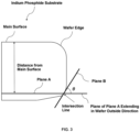
- the indium phosphide substrate according to the present embodiment has an angle ⁇ on the main surface side of 0° ⁇ ⁇ ⁇ 120° for all of the planes A where a distance from the main surface is 100 ⁇ m or more to 200 ⁇ m or less, wherein the angle ⁇ is formed by a plane B, the plane B including an intersection line of an wafer edge with each of the planes A and being tangent to the wafer edge, and an plane of each of the planes A extending in a wafer outside direction.
- each of FIGS. 1-3 shows a cross-sectional schematic view near a wafer edge of an indium phosphide substrate.
- a cross section of the wafer edge of the indium phosphide substrate is curved by cutting (chamfering) corners of the rectangle as shown in each of FIGS. 1-3 . Therefore, the size of the above angle ⁇ varies depending on portions of the wafer taken as the planes A. As the angle ⁇ is close to 180°, the wafer edge will be sharper. It should be noted that each of FIGS.
- the "wafer edge" refers to a side surface of the indium phosphide substrate, i.e., an outer surface excluding the main surface and the back surface.
- the plane A is taken at the center of the wafer in the thickness direction. Therefore, the angle ⁇ formed by the plane B, which includes the intersection line of the wafer edge with the plane A and is tangent to the wafer edge, and a plane of the plane A extending in the wafer outside direction is 90°.
- the plane A is taken at the upper portion of the wafer in the thickness direction.
- the angle ⁇ formed by the plane B which includes the intersection line of the wafer edge with the plane A and is tangent to the wafer edge, and a plane extending from the plane A to the outside of the wafer is an obtuse angle (90° ⁇ ⁇ ⁇ 180°).
- the plane A is taken at the lower portion of the wafer in the thickness direction.
- the angle ⁇ formed by the plane B which includes the intersection line of the wafer edge with the plane A and is tangent to the wafer edge, and a plane extending from the plane A to the outside of the wafer is an acute angle (0° ⁇ ⁇ ⁇ 90°).
- each of the angles ⁇ on the main surface side is controlled to be 0° ⁇ ⁇ ⁇ 120° for all of the planes A where the distance from the main surface is 100 ⁇ m or more to 200 ⁇ m or less.
- the angle ⁇ is preferably controlled to be 60° ⁇ ⁇ ⁇ 120° for all of the planes A where the distance from the main surface is 100 ⁇ m or more to 200 ⁇ m or less.
- the plane B includes the intersection line of the wafer edge with each of the planes A and is tangent to the wafer edge.
- the value of the angle ⁇ on the main surface side formed by the plane B and the plane of the plane A extending in the wafer outside direction varies to some extent depending on a degree of surface roughness of the wafer edge. It is believed that the variation of the angle ⁇ due to the surface roughness of the wafer edge has a very small impact on, in particular, the suppression of the sharpness of the wafer edge that occurs when polishing is carried out from the back surface of the wafer using the method such as back lapping, which is an effect of the present invention.
- Each angle ⁇ defined in the present invention is measured by observing the shape of the wafer edge with Wafer Edge Profile Checker (EPRO-212EO manufactured by YUHI ELECTRONICS) as described below.
- the plane B may be a plane measured at any degree of accuracy that can be measured using the Wafer Edge Profile Checker, regardless of the surface roughness of the wafer edge.
- the planes A are all planes A where the distance from the main surface is 100 ⁇ m or more to 200 ⁇ m or less. This is because the above effect can be obtained to a thickness such that the distance from the main surface is 100 ⁇ m or more to 200 ⁇ m or less, for the indium phosphide substrate polished from the back surface of the wafer by the method such as back lapping. Also, the thickness of the indium phosphide substrate according to the present embodiment is 330 ⁇ m or more to 700 ⁇ m or less.
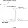
- the indium phosphide substrate according the present embodiment has edge rounds on the main surface side and a surface side opposite to the main surface (back surface side), as shown in FIG. 4 . Further, the chamfered width X f from the wafer edge on the main surface side is controlled to 50 ⁇ m or more to 130 ⁇ m or less, and the chamfered width X b from the wafer edge on the back surface side is controlled to 150 ⁇ m or more to 400 ⁇ m or less.
- the chamfered width X f from the wafer edge on the main surface side is thus controlled to 50 ⁇ m or more to 130 ⁇ m or less, the sharpness of the wafer edge will be suppressed when the indium phosphide substrate is polished from the back surface of the wafer to the plane A by a method such as back lapping. Therefore, it is possible to satisfactorily suppress the generation of damage such as cracks on the wafer edge, for example, during the process. Further, the chamfered width X b from the wafer edge on the back surface side is controlled to 150 ⁇ m or more to 400 ⁇ m or less.
- the designing of the chamfered shapes of the wafer on the main surface side and the back surface side so as to be asymmetrical and the increasing of the chamfered width of the back surface side can ensure a space for inserting a jig such as a scraper into the back surface side. Therefore, after mirror polishing, the wafer can be easily peeled off from the ceramic plate without causing chipping.
- the chamfered width X b from the wafer edge on the back surface side of 150 ⁇ m or more can lead to a wider space for inserting a jig such as a scraper into the back surface side, and can allow the generation of chipping to be satisfactorily suppressed.
- the chamfered width X b from the wafer edge on the back surface side of 400 ⁇ m or less can suppress excessive eroding of the edge shape on the back surface side of the substrate to the front surface side, ensure the chamfered width on the front surface side, and suppress disappearance of a polishing allowance.
- the chamfered width X b from the wafer edge on the back surface side is preferably 160 ⁇ m or more to 340 ⁇ m or less.
- the wafer edge may be configured to include: tapered portions formed to decrease the wafer thickness from each of the main surface side and/or the back surface side; and an edge round smoothly connected to the tapered portions.
- the back surface side of the indium phosphide substrate has a shape provided with the tapered portion.
- the phosphide substrate according to the present embodiment has an angle ⁇ on the main surface side of 60° ⁇ ⁇ ⁇ 110° for all of the planes A where a distance from the main surface is 100 ⁇ m or more to 200 ⁇ m or less, wherein the angle ⁇ is formed by a plane B, the plane B including an intersection line of an wafer edge with each of the planes A and being tangent to the wafer edge, and an plane of each of the planes A extending in a wafer outside direction; wherein in a cross section orthogonal to the wafer edge, the indium phosphide substrate has edge rounds on the main surface side and a surface side opposite to the main surface; wherein a chamfered width X f from the wafer edge on the main surface side is 80 ⁇ m or more to 110 ⁇ m or less; wherein a chamfered width X b from the wafer edge on the surface side opposite
- the sharpness of the wafer edge will be suppressed when the indium phosphide substrate having a diameter of 50.8 mm or less and a thickness of 330 ⁇ m or more to 380 ⁇ m or less is polished from the back surface of the wafer to the plane A by a method such as back lapping. Therefore, it is possible to satisfactorily suppress the generation of damage such as cracks on the wafer edge, for example, during the process. Further, the designing of the chamfered shapes of the wafer on the main surface side and the back surface side so as to be asymmetrical and the increasing of the chamfered width of the back surface side can ensure a space for inserting a jig such as a scraper into the back surface side.
- the chamfered width X b from the wafer edge on the back surface side of 150 ⁇ m or more can lead to a wider space for inserting a jig such as a scraper into the back surface side, and can allow the generation of chipping to be satisfactorily suppressed.
- the chamfered width X b from the wafer edge on the back surface side of 210 ⁇ m or less can suppress excessive eroding of the edge shape on the back surface side of the substrate to the front surface side, ensure the chamfered width on the front surface side, and suppress disappearance of a polishing allowance.
- the chamfered width X b from the wafer edge on the back surface side is preferably 160 ⁇ m or more to 180 ⁇ m or less.
- the phosphide substrate according to the present embodiment has an angle ⁇ on the main surface side of 90° ⁇ ⁇ ⁇ 120° for all of the planes A where a distance from the main surface is 100 ⁇ m or more to 200 ⁇ m or less, wherein the angle ⁇ is formed by a plane B, the plane B including an intersection line of a wafer edge with each of the planes A and being tangent to the wafer edge, and an plane of each of the planes A extending in a wafer outside direction, wherein in a cross section orthogonal to the wafer edge, the indium phosphide substrate has edge rounds on the main surface side and a surface side opposite to the main surface; wherein a chamfered width X f from the wafer edge on the main surface side is 80 ⁇ m or more to 110 ⁇ m or less; wherein a chamfered width X b from the wafer edge on the surface side
- the sharpness of the wafer edge will be suppressed when the indium phosphide substrate having a diameter of 50.8 mm or less and a thickness of 480 ⁇ m or more to 530 ⁇ m or less is polished from the back surface of the wafer to the plane A by a method such as back lapping. Therefore, it is possible to satisfactorily suppress the generation of damage such as cracks on the wafer edge, for example, during the process. Further, the designing of the chamfered shapes of the wafer on the main surface side and the back surface side so as to be asymmetrical and the increasing of the chamfered width of the back surface side can ensure a space for inserting a jig such as a scraper into the back surface side.
- the chamfered width X b from the wafer edge on the back surface side of 180 ⁇ m or more can lead to a wider space for inserting a jig such as a scraper into the back surface side, and can allow the generation of chipping to be satisfactorily suppressed.
- the chamfered width X b from the wafer edge on the back surface side of 230 ⁇ m or less can suppress excessive eroding of the edge shape on the back surface side of the substrate to the front surface side, ensure the chamfered width on the front surface side, and suppress disappearance of a polishing allowance.
- the chamfered width X b from the wafer edge on the back surface side is preferably 190 ⁇ m or more to 210 ⁇ m or less.
- the phosphide substrate according to the present embodiment has an angle ⁇ on the main surface side of 90° ⁇ ⁇ ⁇ 120° for all of the planes A where a distance from the main surface is 100 ⁇ m or more to 200 ⁇ m or less, wherein the angle ⁇ is formed by a plane B, the plane B including an intersection line of an wafer edge with each of the planes A and being tangent to the wafer edge, and an plane of each of the planes A extending in a wafer outside direction, wherein in a cross section orthogonal to the wafer edge, the indium phosphide substrate has edge rounds on the main surface side and a surface side opposite to the main surface; wherein a chamfered width X f from the wafer edge on the main surface side is 90 ⁇ m or more to 130 ⁇ m or less; wherein a chamfered width X b from the wafer edge on the surface side opposite
- the sharpness of the wafer edge will be suppressed when the indium phosphide substrate having a diameter of 76.2 mm or less and a thickness of 570 ⁇ m or more to 630 ⁇ m or less is polished from the back surface of the wafer to the plane A by a method such as back lapping. Therefore, it is possible to satisfactorily suppress the generation of damage such as cracks on the wafer edge, for example, during the process. Further, the designing of the chamfered shapes of the wafer on the main surface side and the back surface side so as to be asymmetrical and the increasing of the chamfered width of the back surface side can ensure a space for inserting a jig such as a scraper into the back surface side.
- the chamfered width X b from the wafer edge on the back surface side of 270 ⁇ m or more can lead to a wider space for inserting a jig such as a scraper into the back surface side, and can allow the generation of chipping to be satisfactorily suppressed.
- the chamfered width X b from the wafer edge on the back surface side of 350 ⁇ m or less can suppress excessive eroding of the edge shape on the back surface side of the substrate to the front surface side, ensure the chamfered width on the front surface side, and suppress disappearance of a polishing allowance.
- the chamfered width X b from the wafer edge on the back surface side is preferably 280 ⁇ m or more to 340 ⁇ m or less.
- the method for producing the indium phosphide substrate starts from producing an indium phosphide ingot by a known method.
- the indium phosphide ingot is then ground into a cylinder.
- a wafer having a main surface and a back surface is then cut out from the ground indium phosphide ingot.
- both ends of the crystal of the indium phosphide ingot are cut along a predetermined crystal plane using a wire saw to cut out a plurality of wafers to have a predetermined thickness.
- both surfaces of the cut wafer are etched with a predetermined etching solution (primary etching).
- the wafer can be etched by immersing the entire wafer in the etching solution.
- an outer peripheral portion of the wafer is chamfered, and at least one surface, preferably both surfaces, of the chamfered wafer is polished.
- the polishing step is also called a lapping step, and the wafer is polished with certain abrasives to remove irregularities on the wafer surface while maintaining the flatness of the wafer.
- Both surfaces of the polished wafer are then etched with a predetermined etching solution (secondary etching).
- the wafer can be etched by immersing the entire wafer in the etching solution.
- the main surface of the wafer is then polished with an abrasive material for mirror polishing to finish it into a mirror surface while attaching a plate such as a ceramic plate to the back surface of the wafer.
- polishing is carried out by rotating and revolving the wafer while sandwiching it between upper and lower surface plates, and then the polishing may be carried out while attaching the wafer to the ceramic plate or the like using the same method as described above for the purposes of reducing processing damage during the polishing of the both surfaces and removing minute scratches on the surface.
- a jig such as a scraper is inserted into the back surface side to peel off the plate.
- the resulting polished wafer is then washed to produce an indium phosphide substrate according to an embodiment of the present invention.
- the shape of the wafer edge may be controlled by adjusting a chamfered amount as appropriate based on an amount of the wafer to be cut during the lapping, etching, and polishing as described above.
- the chamfered amount (chamfered width from the wafer edge) on the main surface side of the wafer is in the range of from 150 to 320 ⁇ m, and the chamfered amount on the back surface side is in the range of 320 to 580 ⁇ m.
- the removal is carried out such that the removed (polished) amount on the main surface side of the chamfered wafer is in the range of 80 ⁇ m or less in the wafer thickness direction, and the removed amount on the back surface side is in the range of 70 ⁇ m or less in the wafer thickness direction, so that for all the planes A where the distance from the main surface is in the defined range, each angle ⁇ on the main surface side formed by the plane B which is tangent to the wafer edge as described above, and the plane of each of the planes A extending in the wafer outside direction can be controlled as needed. Further, the generation of chipping on the back surface side can be suppressed when the wafer is peeled off from the ceramic plate or the like, which has been attached to the back surface side of the wafer.
- an epitaxial crystal layer By epitaxially growing a semiconductor thin film onto the main surface of the indium phosphide substrate according to the embodiment of the present invention by a known method, an epitaxial crystal layer can be formed to produce a semiconductor epitaxial wafer.
- an InAIAs buffer layer, an InGaAs channel layer, an InAIAs spacer layer and an InP electron supply layer may be epitaxially grown onto the main surface of the indium phosphide substrate to form a HEMT structure.
- a mirror-finished indium phosphide substrate is etched with an etching solution such as sulfuric acid/hydrogen peroxide solution to remove impurities such as silicon (Si) adhering to the substrate surface.
- an etching solution such as sulfuric acid/hydrogen peroxide solution to remove impurities such as silicon (Si) adhering to the substrate surface.
- the back surface of the etched indium phosphide substrate is brought into contact with the susceptor and supported, and in this state, an epitaxial film is formed on the main surface of the indium phosphide substrate by molecular beam epitaxy (MBE) or metal organic chemical vapor deposition (MOCVD).
- MBE molecular beam epitaxy
- MOCVD metal organic chemical vapor deposition
- Examples 1 to 4 and Comparative Examples 1 to 2 were prepared as follows: First, ingots of indium phosphide monocrystals grown with a predetermined diameter were prepared.
- a wafer having a main surface and a back surface was cut out from the ground indium phosphide ingot.
- both ends of the crystal of the indium phosphide ingot were cut along a predetermined crystal plane using a wire saw to cut out a plurality of wafers to have a predetermined thickness.
- a new wire was continuously delivered while reciprocating the wire, and the indium phosphide ingot was moved toward a wire saw.
- the cut wafer was etched from both sides with a mixed solution of 85% by mass of an aqueous phosphoric acid solution and 30% by mass of a hydrogen peroxide solution (primary etching).
- the wafer was etched by immersing the entire wafer in the etching solution.
- an outer peripheral portion of the wafer was chamfered. Both surfaces of the chamfered wafer were then polished (lapped). In this case, the wafer was polished with abrasives to remove irregularities on the wafer surface while maintaining the flatness of the wafer.
- Both surfaces of the polished wafer was then etched with a mixed solution of 85% by mass of an aqueous phosphoric acid solution, 30% by mass of a hydrogen peroxide solution and ultrapure water (secondary etching).
- the wafer was etched by immersing the entire wafer in the etching solution.
- the main surface of the wafer was then polished with abrasives for mirror polishing to finish it into a mirror surface while attaching a ceramic plate to the back surface of the wafer.
- the polishing was carried out while attaching the ceramic plate to the back surface of the wafer using the same method as described above for the purposes of reducing processing damage during the polishing of the both surfaces and removing minute scratches on the surface.
- a jig such as a scraper was inserted into the back surface side to peel off the plate.
- washing was carried out to produce an indium phosphide substrate.
- each wafer production is adjusted such that when the planes A parallel to the main surface of the wafer are taken in the wafer, the angle ⁇ formed by the plane B, which includes the intersection line of the wafer edge with each of the planes A and is tangent to the wafer edge, and the plane of each of the planes A extending in the wafer outside direction is in the defined range for the plane A at the predetermined distance from the main surface. Also, each wafer production was adjusted such that each of the chamfered widths X f , X b from the wafer edges of the front surface and the back surface was in the defined range. For each wafer shape in Table 1, reference may be made to the schematic cross-sectional view near the wafer edge of the indium phosphide substrate as shown in FIG. 5 .
- Each of the edges of the wafers according to Examples 1 to 4 and Comparative Examples 1 to 2 were measured using Wafer Edge Profile Checker (EPRO-212EO from YUHI ELECTRONICS).
- Each of the angles ( ⁇ 1 , ⁇ 2 , ⁇ 3 ) was calculated by drawing a straight line A parallel to the main surface (corresponding to the plane A), which corresponded to the thickness after back lapping, drawing a tangent line B where a contact point of the straight line A with the wafer edge was a tangent point (corresponding to plane B), and determining the angle formed by the straight line A and the tangent line B.
- the chipping on the back surface is affected only by two factors: the chamfered width X b from the wafer edge on the back surface and the wafer thickness. Therefore, it is believed that even for wafers having larger diameters than those of Examples 3 and 4, the generation of chipping can be suppressed by similarly controlling only the two factors: the chamfered width X b and the wafer thickness.
Landscapes
- Chemical & Material Sciences (AREA)
- Engineering & Computer Science (AREA)
- Crystallography & Structural Chemistry (AREA)
- Materials Engineering (AREA)
- Metallurgy (AREA)
- Organic Chemistry (AREA)
- Inorganic Chemistry (AREA)
- Mechanical Treatment Of Semiconductor (AREA)
Applications Claiming Priority (2)
| Application Number | Priority Date | Filing Date | Title |
|---|---|---|---|
| JP2021145784A JP7055233B1 (ja) | 2021-09-07 | 2021-09-07 | リン化インジウム基板 |
| PCT/JP2022/009815 WO2023037597A1 (ja) | 2021-09-07 | 2022-03-07 | リン化インジウム基板 |
Publications (2)
| Publication Number | Publication Date |
|---|---|
| EP4170700A1 true EP4170700A1 (de) | 2023-04-26 |
| EP4170700A4 EP4170700A4 (de) | 2024-01-03 |
Family
ID=85478243
Family Applications (1)
| Application Number | Title | Priority Date | Filing Date |
|---|---|---|---|
| EP22725154.3A Pending EP4170700A4 (de) | 2021-09-07 | 2022-03-07 | Indiumphosphidsubstrat |
Country Status (3)
| Country | Link |
|---|---|
| US (1) | US12065759B2 (de) |
| EP (1) | EP4170700A4 (de) |
| CN (1) | CN116097404A (de) |
Family Cites Families (13)
| Publication number | Priority date | Publication date | Assignee | Title |
|---|---|---|---|---|
| JP3368799B2 (ja) * | 1997-05-22 | 2003-01-20 | 住友電気工業株式会社 | Iii−v族化合物半導体ウェハおよびその製造方法 |
| EP1189266B1 (de) | 2000-03-29 | 2017-04-05 | Shin-Etsu Handotai Co., Ltd. | Methode zur herstellung einer siliziumhalbleiterscheibe und einer soi-scheibe soiwe soi-scheibe |
| JP4162892B2 (ja) | 2002-01-11 | 2008-10-08 | 日鉱金属株式会社 | 半導体ウェハおよびその製造方法 |
| JP2003218033A (ja) | 2002-01-21 | 2003-07-31 | Nikko Materials Co Ltd | エピタキシャル成長方法 |
| JP2006203071A (ja) | 2005-01-21 | 2006-08-03 | Sumitomo Electric Ind Ltd | Iii−v族化合物半導体単結晶基板 |
| JP2007042748A (ja) | 2005-08-01 | 2007-02-15 | Hitachi Cable Ltd | 化合物半導体ウェハ |
| JP2008177233A (ja) | 2007-01-16 | 2008-07-31 | Hitachi Cable Ltd | 化合物半導体ウェハ及びその製造方法 |
| JP5934491B2 (ja) * | 2011-10-25 | 2016-06-15 | 株式会社ディスコ | サファイア基板の研削方法 |
| JP6035982B2 (ja) * | 2012-08-09 | 2016-11-30 | 株式会社Sumco | エピタキシャルシリコンウェーハの製造方法およびエピタキシャルシリコンウェーハ |
| EP3476983A4 (de) * | 2017-04-28 | 2020-04-01 | JX Nippon Mining & Metals Corporation | Halbleiterwafer und verfahren zum polieren von halbleiterwafern |
| JP7021632B2 (ja) * | 2018-12-27 | 2022-02-17 | 株式会社Sumco | ウェーハの製造方法およびウェーハ |
| JP7158594B2 (ja) | 2020-01-29 | 2022-10-21 | Jx金属株式会社 | リン化インジウム基板 |
| CN113206007B (zh) | 2021-04-30 | 2022-02-22 | 中锗科技有限公司 | 一种磷化铟衬底的制备方法 |
-
2022
- 2022-03-07 EP EP22725154.3A patent/EP4170700A4/de active Pending
- 2022-03-07 CN CN202280001864.8A patent/CN116097404A/zh active Pending
- 2022-03-07 US US17/787,197 patent/US12065759B2/en active Active
Also Published As
| Publication number | Publication date |
|---|---|
| US12065759B2 (en) | 2024-08-20 |
| US20230082020A1 (en) | 2023-03-16 |
| CN116097404A (zh) | 2023-05-09 |
| EP4170700A4 (de) | 2024-01-03 |
Similar Documents
| Publication | Publication Date | Title |
|---|---|---|
| EP3933077A1 (de) | Indiumphosphidsubstrat | |
| EP3862134B1 (de) | Verfahren zur herstellung von indiumphosphidsubstrat | |
| EP3933891A1 (de) | Indiumphosphid substrat und verfahren zur herstellung von indiumphosphid substrat | |
| US20220199770A1 (en) | Indium phosphide substrate and method for producing indium phosphide substrate | |
| EP3862133B1 (de) | Verfahren zur herstellung eines indiumphosphid-substrats | |
| EP3862132B1 (de) | Verfahren zur herstellung eines indiumphosphid-substrats | |
| EP4215650A1 (de) | Indiumphosphidsubstrat, verfahren zur herstellung eines indiumphosphidsubstrats und epitaktischer halbleiterwafer | |
| TWI810847B (zh) | 磷化銦基板 | |
| EP4170700A1 (de) | Indiumphosphidsubstrat | |
| EP4207249A1 (de) | Indiumphosphidsubstrat, verfahren zur herstellung eines indiumphosphidsubstrats und epitaktischer halbleiterwafer | |
| EP4582602A1 (de) | Indiumphosphidsubstrat und halbleiterepitaxialwafer | |
| WO2025203752A1 (ja) | リン化インジウム基板及び半導体エピタキシャルウエハ | |
| WO2025104949A1 (ja) | リン化インジウム基板及び半導体エピタキシャルウエハ |
Legal Events
| Date | Code | Title | Description |
|---|---|---|---|
| STAA | Information on the status of an ep patent application or granted ep patent |
Free format text: STATUS: UNKNOWN |
|
| STAA | Information on the status of an ep patent application or granted ep patent |
Free format text: STATUS: THE INTERNATIONAL PUBLICATION HAS BEEN MADE |
|
| PUAI | Public reference made under article 153(3) epc to a published international application that has entered the european phase |
Free format text: ORIGINAL CODE: 0009012 |
|
| STAA | Information on the status of an ep patent application or granted ep patent |
Free format text: STATUS: REQUEST FOR EXAMINATION WAS MADE |
|
| 17P | Request for examination filed |
Effective date: 20220601 |
|
| AK | Designated contracting states |
Kind code of ref document: A1 Designated state(s): AL AT BE BG CH CY CZ DE DK EE ES FI FR GB GR HR HU IE IS IT LI LT LU LV MC MK MT NL NO PL PT RO RS SE SI SK SM TR |
|
| A4 | Supplementary search report drawn up and despatched |
Effective date: 20231204 |
|
| RIC1 | Information provided on ipc code assigned before grant |
Ipc: H01L 21/02 20060101ALI20231128BHEP Ipc: H01L 21/304 20060101AFI20231128BHEP |
|
| DAV | Request for validation of the european patent (deleted) | ||
| DAX | Request for extension of the european patent (deleted) |