EP4170706A1 - Procédé de production d'une puce de circuit intégré comprenant un réseau de distribution d'énergie arrière - Google Patents
Procédé de production d'une puce de circuit intégré comprenant un réseau de distribution d'énergie arrière Download PDFInfo
- Publication number
- EP4170706A1 EP4170706A1 EP21203706.3A EP21203706A EP4170706A1 EP 4170706 A1 EP4170706 A1 EP 4170706A1 EP 21203706 A EP21203706 A EP 21203706A EP 4170706 A1 EP4170706 A1 EP 4170706A1
- Authority
- EP
- European Patent Office
- Prior art keywords
- layer
- rails
- trenches
- sacrificial
- back side
- Prior art date
- Legal status (The legal status is an assumption and is not a legal conclusion. Google has not performed a legal analysis and makes no representation as to the accuracy of the status listed.)
- Pending
Links
Images

Classifications
-
- H—ELECTRICITY
- H10—SEMICONDUCTOR DEVICES; ELECTRIC SOLID-STATE DEVICES NOT OTHERWISE PROVIDED FOR
- H10W—GENERIC PACKAGES, INTERCONNECTIONS, CONNECTORS OR OTHER CONSTRUCTIONAL DETAILS OF DEVICES COVERED BY CLASS H10
- H10W20/00—Interconnections in chips, wafers or substrates
- H10W20/01—Manufacture or treatment
- H10W20/031—Manufacture or treatment of conductive parts of the interconnections
- H10W20/056—Manufacture or treatment of conductive parts of the interconnections by filling conductive material into holes, grooves or trenches
-
- H—ELECTRICITY
- H10—SEMICONDUCTOR DEVICES; ELECTRIC SOLID-STATE DEVICES NOT OTHERWISE PROVIDED FOR
- H10W—GENERIC PACKAGES, INTERCONNECTIONS, CONNECTORS OR OTHER CONSTRUCTIONAL DETAILS OF DEVICES COVERED BY CLASS H10
- H10W20/00—Interconnections in chips, wafers or substrates
- H10W20/01—Manufacture or treatment
- H10W20/021—Manufacture or treatment of interconnections within wafers or substrates
- H10W20/023—Manufacture or treatment of interconnections within wafers or substrates the interconnections being through-semiconductor vias
-
- H—ELECTRICITY
- H10—SEMICONDUCTOR DEVICES; ELECTRIC SOLID-STATE DEVICES NOT OTHERWISE PROVIDED FOR
- H10P—GENERIC PROCESSES OR APPARATUS FOR THE MANUFACTURE OR TREATMENT OF DEVICES COVERED BY CLASS H10
- H10P54/00—Cutting or separating of wafers, substrates or parts of devices
-
- H—ELECTRICITY
- H10—SEMICONDUCTOR DEVICES; ELECTRIC SOLID-STATE DEVICES NOT OTHERWISE PROVIDED FOR
- H10P—GENERIC PROCESSES OR APPARATUS FOR THE MANUFACTURE OR TREATMENT OF DEVICES COVERED BY CLASS H10
- H10P74/00—Testing or measuring during manufacture or treatment of wafers, substrates or devices
- H10P74/20—Testing or measuring during manufacture or treatment of wafers, substrates or devices characterised by the properties tested or measured, e.g. structural or electrical properties
- H10P74/203—Structural properties, e.g. testing or measuring thicknesses, line widths, warpage, bond strengths or physical defects
-
- H—ELECTRICITY
- H10—SEMICONDUCTOR DEVICES; ELECTRIC SOLID-STATE DEVICES NOT OTHERWISE PROVIDED FOR
- H10W—GENERIC PACKAGES, INTERCONNECTIONS, CONNECTORS OR OTHER CONSTRUCTIONAL DETAILS OF DEVICES COVERED BY CLASS H10
- H10W20/00—Interconnections in chips, wafers or substrates
- H10W20/01—Manufacture or treatment
- H10W20/021—Manufacture or treatment of interconnections within wafers or substrates
-
- H—ELECTRICITY
- H10—SEMICONDUCTOR DEVICES; ELECTRIC SOLID-STATE DEVICES NOT OTHERWISE PROVIDED FOR
- H10W—GENERIC PACKAGES, INTERCONNECTIONS, CONNECTORS OR OTHER CONSTRUCTIONAL DETAILS OF DEVICES COVERED BY CLASS H10
- H10W20/00—Interconnections in chips, wafers or substrates
- H10W20/01—Manufacture or treatment
- H10W20/021—Manufacture or treatment of interconnections within wafers or substrates
- H10W20/023—Manufacture or treatment of interconnections within wafers or substrates the interconnections being through-semiconductor vias
- H10W20/0245—Manufacture or treatment of interconnections within wafers or substrates the interconnections being through-semiconductor vias comprising use of blind vias during the manufacture
-
- H—ELECTRICITY
- H10—SEMICONDUCTOR DEVICES; ELECTRIC SOLID-STATE DEVICES NOT OTHERWISE PROVIDED FOR
- H10W—GENERIC PACKAGES, INTERCONNECTIONS, CONNECTORS OR OTHER CONSTRUCTIONAL DETAILS OF DEVICES COVERED BY CLASS H10
- H10W20/00—Interconnections in chips, wafers or substrates
- H10W20/01—Manufacture or treatment
- H10W20/021—Manufacture or treatment of interconnections within wafers or substrates
- H10W20/023—Manufacture or treatment of interconnections within wafers or substrates the interconnections being through-semiconductor vias
- H10W20/0257—Manufacture or treatment of interconnections within wafers or substrates the interconnections being through-semiconductor vias comprising using a sacrificial placeholder, e.g. using a sacrificial plug
-
- H—ELECTRICITY
- H10—SEMICONDUCTOR DEVICES; ELECTRIC SOLID-STATE DEVICES NOT OTHERWISE PROVIDED FOR
- H10W—GENERIC PACKAGES, INTERCONNECTIONS, CONNECTORS OR OTHER CONSTRUCTIONAL DETAILS OF DEVICES COVERED BY CLASS H10
- H10W20/00—Interconnections in chips, wafers or substrates
- H10W20/01—Manufacture or treatment
- H10W20/071—Manufacture or treatment of dielectric parts thereof
- H10W20/081—Manufacture or treatment of dielectric parts thereof by forming openings in the dielectric parts
-
- H—ELECTRICITY
- H10—SEMICONDUCTOR DEVICES; ELECTRIC SOLID-STATE DEVICES NOT OTHERWISE PROVIDED FOR
- H10W—GENERIC PACKAGES, INTERCONNECTIONS, CONNECTORS OR OTHER CONSTRUCTIONAL DETAILS OF DEVICES COVERED BY CLASS H10
- H10W20/00—Interconnections in chips, wafers or substrates
- H10W20/20—Interconnections within wafers or substrates, e.g. through-silicon vias [TSV]
- H10W20/211—Through-semiconductor vias, e.g. TSVs
- H10W20/218—Through-semiconductor vias, e.g. TSVs in silicon-on-insulator [SOI] wafers
-
- H—ELECTRICITY
- H10—SEMICONDUCTOR DEVICES; ELECTRIC SOLID-STATE DEVICES NOT OTHERWISE PROVIDED FOR
- H10W—GENERIC PACKAGES, INTERCONNECTIONS, CONNECTORS OR OTHER CONSTRUCTIONAL DETAILS OF DEVICES COVERED BY CLASS H10
- H10W20/00—Interconnections in chips, wafers or substrates
- H10W20/40—Interconnections external to wafers or substrates, e.g. back-end-of-line [BEOL] metallisations or vias connecting to gate electrodes
- H10W20/41—Interconnections external to wafers or substrates, e.g. back-end-of-line [BEOL] metallisations or vias connecting to gate electrodes characterised by their conductive parts
- H10W20/427—Power or ground buses
-
- H—ELECTRICITY
- H10—SEMICONDUCTOR DEVICES; ELECTRIC SOLID-STATE DEVICES NOT OTHERWISE PROVIDED FOR
- H10D—INORGANIC ELECTRIC SEMICONDUCTOR DEVICES
- H10D84/00—Integrated devices formed in or on semiconductor substrates that comprise only semiconducting layers, e.g. on Si wafers or on GaAs-on-Si wafers
- H10D84/01—Manufacture or treatment
- H10D84/0123—Integrating together multiple components covered by H10D12/00 or H10D30/00, e.g. integrating multiple IGBTs
- H10D84/0126—Integrating together multiple components covered by H10D12/00 or H10D30/00, e.g. integrating multiple IGBTs the components including insulated gates, e.g. IGFETs
- H10D84/0165—Integrating together multiple components covered by H10D12/00 or H10D30/00, e.g. integrating multiple IGBTs the components including insulated gates, e.g. IGFETs the components including complementary IGFETs, e.g. CMOS devices
- H10D84/0186—Manufacturing their interconnections or electrodes, e.g. source or drain electrodes
-
- H—ELECTRICITY
- H10—SEMICONDUCTOR DEVICES; ELECTRIC SOLID-STATE DEVICES NOT OTHERWISE PROVIDED FOR
- H10D—INORGANIC ELECTRIC SEMICONDUCTOR DEVICES
- H10D84/00—Integrated devices formed in or on semiconductor substrates that comprise only semiconducting layers, e.g. on Si wafers or on GaAs-on-Si wafers
- H10D84/01—Manufacture or treatment
- H10D84/02—Manufacture or treatment characterised by using material-based technologies
- H10D84/03—Manufacture or treatment characterised by using material-based technologies using Group IV technology, e.g. silicon technology or silicon-carbide [SiC] technology
- H10D84/038—Manufacture or treatment characterised by using material-based technologies using Group IV technology, e.g. silicon technology or silicon-carbide [SiC] technology using silicon technology, e.g. SiGe
-
- H—ELECTRICITY
- H10—SEMICONDUCTOR DEVICES; ELECTRIC SOLID-STATE DEVICES NOT OTHERWISE PROVIDED FOR
- H10W—GENERIC PACKAGES, INTERCONNECTIONS, CONNECTORS OR OTHER CONSTRUCTIONAL DETAILS OF DEVICES COVERED BY CLASS H10
- H10W20/00—Interconnections in chips, wafers or substrates
- H10W20/01—Manufacture or treatment
- H10W20/031—Manufacture or treatment of conductive parts of the interconnections
- H10W20/0698—Local interconnections
Definitions
- the present invention is related to integrated circuit chips, hereafter abbreviated to ICs or IC chips, in particular to the aspect of the delivery of power to the active devices on the chip.
- the nanoTSVs however represent a restriction in terms of the resistivity of the power supply path to the active devices on the front side. Also, as buried power rails are processed from the font side of a device wafer, the material choice for these buried rails is limited to materials which are compatible with the thermal budget for front side processing. This excludes a number of low-resistivity materials.
- contact resistances are another ongoing concern in the development of IC chip designs.
- the contact resistance between nanoTSVs and back side power supply tracks is often unsatisfactory because of the material choices and dimensional restrictions related to TSV processing.
- the invention aims to provide a solution to the problems highlighted above. This is achieved by a method for producing an IC chip in accordance with the appended claims.
- a method for producing an IC chip in accordance with the appended claims.
- deep trenches are formed in a semiconductor layer that forms the top layer of a device wafer, the trenches going through the complete thickness of the layer.
- the trenches are filled with a sacrificial material, that is subsequently etched back and covered with a capping layer thereby forming sacrificial buried rails.
- the device wafer After processing the active devices of the IC on the front surface of the semiconductor layer, including connections to the sacrificial rails, the device wafer is bonded face down to a carrier wafer, and thinned from the back side, until the sacrificial rails are exposed.
- the sacrificial material and the capping layer are removed and replaced by a conductive material, thereby forming the actual buried power rails.
- This is followed by further back side processing to form a back side power delivery network to supply power through the buried rails to the active devices of the IC.
- a sacrificial material for the buried rails enables a wider choice of materials for these buried rails.
- the invention is in particular related to a method for producing an integrated circuit chip, comprising the steps of :
- the device wafer comprises a base wafer, an etch stop layer on the base wafer, and said semiconductor layer on the etch stop layer, wherein the etch stop function of the etch stop layer is related to stopping an etch process applied during said step of thinning the device wafer from the back side thereof.
- the deep parallel trenches reach into the etch stop layer.
- the deep parallel trenches are formed through the complete thickness of the etch stop layer and into the base wafer.
- a spectrometry method is used to monitor the depth of the trenches, as these trenches are being formed using an etch process, by detecting materials released from the semiconductor layer and from the etch stop layer.
- the active devices are fin-based devices or nano-sheet based devices and wherein the buried power rails run parallel to the fins or to the nano-sheets of said active devices.
- the sacrificial material is tungsten or amorphous silicon.
- the capping layer is a dielectric layer.
- the capping layer is a silicon nitride layer.
- the method according to the invention is described on the basis of one embodiment of the method, for producing an integrated circuit chip comprising a CMOS layout of finFET transistors arranged in standard cells on a semiconductor substrate.
- the invention is not limited to this particular application field, as will be made clearer after the description of the embodiment in question. Any reference to materials used for the various layers and areas that will be described is merely intended as an example of suitable materials and is not to be understood as a limitation of the scope of the present invention.
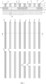
- Figure 1 shows a small portion of a device wafer (i.e., a wafer onto which active devices of IC chips are to be processed), comprising a monocrystalline Si layer 1, into which a number of fins 2 and 2' have been produced by a known lithography and etch technique, applying etch masks 3.
- the width of the fins may be in the order of 10 nm or less.
- the two different types of hatching indicate different doping types (referred to also by respective references 2 and 2'), typically p-type and n-type doping.
- the Si layer 1 could be a p-type layer, implanted with n-type dopants in well-areas 4.
- the well-areas 4 reach about half the depth of the Si layer 1 but could also reach to the back surface of the Si layer.
- the image is merely a schematic indication of the fact that adjacent p- and n-areas are created on the device wafer.
- This layout is typically used for producing pMOS and nMOS transistors arranged in multiple standard cells.
- the layout comprises regularly spaced pairs of fins arranged in alternate groups of four p-type fins 2 and four n-type fins 2'. As seen in the plane view in Figure 1 , the fins are cut in their length direction in accordance with a suitable layout for an area of the IC chip that is to be processed in said area.
- the Si layer 1 is a monocrystalline top layer of a multi-layer device wafer comprising a base wafer 5, typically a Si wafer, and a thin etch stop layer 6, which could be a SiGe layer.
- the Si layer 1 (including the fins) preferably has a thickness less than 1 ⁇ m, for example about 500 nm.
- the etch stop layer 6 may be a SiGe layer of about 50nm thick for example. Its function as an etch stop layer is to stop the etching of the base wafer 5 from the back side, as will be explained later in this description.
- the SiGe layer 6 and the monocrystalline Si layer 1 may be produced on a Si base wafer 5 by techniques well known in the art, preferably by epitaxial growth methods.
- the fins 2, 2' are embedded in a layer 7 of dielectric material. Typically, this is a layer of silicon oxide (SiO 2 ), also referred to as 'shallow trench isolation' oxide.
- SiO 2 silicon oxide
- Layer 7 may be applied by any known technique, that may include a densification anneal step applying a thermal budget that is compatible with the material of the etch stop layer 6.
- the STI layer 7 may include a liner that follows the topography of the fins, for example a thin SiN layer, with a SiO 2 deposited on top of the SiN layer.
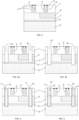
- Figure 2 is an enlarged image of the part of the section view of Figure 1 indicated by the rectangle R, including two p-type fins 2 and two n-type fins 2'.
- deep trenches 10 are etched by anisotropic etching through the complete thickness of the Si layer 1, in the areas between consecutive pairs of fins of the same type in Figure 1 , i.e., on either side of the two pairs of fins shown in Figure 2 . In their length direction, the trenches 10 span across a given area of the fin layout of which a part is shown in the plane view of Figure 1 .
- the width of the trenches 10 is shown to be significantly larger than the width of the fins 2,2' but this is mostly in order to be able to clearly show a number of aspects of the method later on. In reality the trenches 10 could be narrower than shown in the drawings.
- the trenches 10 may reach into the SiGe layer 6 as illustrated in Figure 3a or pass through the SiGe layer 6 and partially into the base wafer 5, as illustrated in Figure 3b .
- the formation of these trenches is typically realised by lithography and etch techniques known as such in the art and therefore not described here in detail.
- the etch stop function does not refer in the first place to etch recipes for producing the trenches 10. So, while it would be possible to use a first etch recipe for etching Si selectively to SiGe, i.e., an etch process that stops on the SiGe layer 6 and thereafter another etch recipe that allows to continue the etch process into and possibly through the SiGe layer 6, it is also possible to use an etch recipe that removes both Si and SiGe.
- such an etch recipe is used that removes both Si and SiGe, and the material that is released from the Si layer 1 and from the SiGe layer 6 during the etch process is monitored by spectrometry as the etch progresses, so that the time may be detected when the SiGe layer 6 is reached.
- the etch process could then be stopped or continued further into the SiGe layer (as in Figure 3a ), or fully through the SiGe layer and into the base wafer 5 (as in Figure 3b ).
- a timed etch can be applied, wherein the etch time is determined beforehand based on known etch speeds and the dimensions of the etched areas.
- the spectrometry-based approach however enables to obtain a more accurate control of the depth of the trenches 10.
- This spectrometry-based monitoring has not been used in this particular context, i.e., for controlling the etch depth of trenches applied for the purpose of producing buried power rails of an IC chip.
- the approach is possible here because the trenches 10 are etched through the complete thickness of the semiconductor layer 1, whereas prior art techniques include etching only partially into the layer 1 and possibly locally continuing the etch to form via openings to the back of the layer 1.
- the amount of released material is sufficient to enable the spectrometry-based monitoring approach described above. Any known spectrometry equipment configured to detect the materials in question could be used for this purpose.
- a dielectric liner 11 is formed on the inner surfaces of the trenches 10, i.e., on the bottom and the sidewalls. This could be a layer of titanium nitride formed by atomic layer deposition (ALD). The thickness of the liner 11 is in accordance with thicknesses generally applied for dielectric liners formed around buried power rails to isolate the rails from the surrounding material.
- a sacrificial material 12 i.e., a material that is to be removed again later in the process.
- the upper surface of the device wafer is then planarized using a suitable planarization technique known in the art, such as CMP (chemical mechanical polishing), resulting in the image shown in Figure 4 .
- the sacrificial material 12 could a metal such as tungsten (W), deposited by ALD or chemical vapour deposition, or a non-metal such as amorphous silicon.
- the sacrificial material is then etched back from the front side of the device wafer, for example (and as shown in the drawings) to just above the base of the fins 2,2'.
- the remaining thickness of sacrificial material corresponds to a suitable thickness for the buried power rails that will ultimately replace the sacrificial material.
- the remaining volumes of the sacrificial material will be referred to as 'sacrificial rails' 13.
- shallow trenches 14 meaning shallower than the original trenches 10) appear above the sacrificial rails 13.
- a capping layer 15 is applied on the inner surfaces of the shallow trenches 14, i.e., on the bottom and sidewalls thereof.
- the capping layer 15 is preferably a dielectric layer and could be a thin SiN layer applied for example by ALD.
- the thickness of the capping layer 15 is in the same order of magnitude as the thickness of the dielectric liner 11.
- the function of the capping layer 15 is to protect the sacrificial rails 13 during front side processing applied for producing active devices and connections from these devices to the sacrificial rails (see further). Any material that is suitable for performing this function can be used as the capping layer.
- the capping layer thus enables the full decoupling of the front side processing steps from the formation of the actual buried rails (see further), so that a wider choice of materials for these rails becomes available.
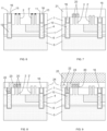
- the shallow trenches 14 are then filled with a dielectric material 16, possibly this may be the same material as the STI layer 7, for example SiO 2 , applied by the same method that may include a densification anneal compatible with the SiGe etch stop layer 6, and the wafer is again planarized, resulting in the view shown in Figure 6 .
- a dielectric material 16 possibly this may be the same material as the STI layer 7, for example SiO 2 , applied by the same method that may include a densification anneal compatible with the SiGe etch stop layer 6, and the wafer is again planarized, resulting in the view shown in Figure 6 .
- CMOS process steps is performed, of which the result is illustrated in a simplified way in Figure 7 .
- This is the processing of source or drain (S/D) contacts 20 of transistors on the fins 2,2', in accordance with a given layout of standard cells arranged between the sacrificial rails 13.
- the STI layer 7 is etched back to expose the top of the fins, and the S/D contacts 20 are formed thereon by epitaxial techniques well known in the art. Contacts are shown only on the p-type fins 2 in the drawing. The n-type fins may equally be provided with contacts lying outside the plane of the drawing. Additional steps for forming transistors or other active devices are performed, such as gate processing steps (not shown). The active devices are covered by another dielectric layer 21 followed by a planarization step.
- Figure 8 shows the result of additional process steps which are known as such, but which are performed normally when buried power rails are already present in the Si layer 1, as opposed to the sacrificial rails 13 formed according to the method of the invention.
- These process steps are sometimes referred to as the formation of a 'VPBR' (via to BPR) 22 and MOA connection 23 (electrically conductive connection to S/D contacts).
- the VPBR and the MOA are drawn as one integral area, and it is in fact possible to form this area in one deposition step.
- the VBPR and the MOA can also be formed in separate steps. As stated, such steps are known as such and therefore not detailed here.
- the top area of the device wafer at this stage of the method is referred to as the front end of line portion 24 of the IC.
- the ' ⁇ ' is merely an indicative sign of the location of the FEOL portion 24, without meaning to define an exact border.
- the method continues with the formation of the BEOL portion 25, the latter being a stack of interconnects comprising several metallization levels (M1,M2 etc), including a passivation layer on top (not shown), as well-known in the art.
- the MOA connections 23 are indicated as part of the front end of line portion 24 in the drawings. They could however be regarded as part of the BEOL portion 25 (see further). This distinction has no bearing on the characterising features of the present invention.
- the base wafer 5 is removed by a thinning sequence that may comprise etching and/or grinding steps, ending with a highly selective etch step, preferably a wet etch in the case of a SiGe etch stop layer 6, that effectively stops when reaching the SiGe layer 6.
- a highly selective etch step preferably a wet etch in the case of a SiGe etch stop layer 6, that effectively stops when reaching the SiGe layer 6.
- Such highly selective etch recipes are well known for the selective etch of Si relative to SiGe as well as for other material combinations.
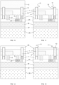
- the etch stop layer 6 itself is removed, resulting in the situation illustrated in Figure 11 , with the sacrificial rails 13, including the liner 11, protruding outward from the back surface of the Si layer 1. If necessary, the material of the Si layer 1 is slightly recessed in order to obtain this result.
- a dielectric layer 30 (e.g. SiO 2 ) is deposited on the wafer and planarized (see Figure 12 ), and thereafter etched back to expose a portion of the sacrificial rails 13. As shown in Figure 13 , said portion may protrude from the dielectric layer 30.
- the liner 11 is removed from the protruding portion of the rails 13, and the sacrificial rails 13 themselves are removed relative to the liner 11 and the capping layer 15, resulting in the view shown in Figure 14 .
- the sacrificial rails 13 are formed of W, the W may be removed using an APM (ammonia peroxide mixture) solution. The removal of the sacrificial rails results in trenches 31 formed through the back surface of the Si layer 1, with the capping layer 15 forming the bottom of these back side trenches 31.
- the capping layer 15 is then removed from the bottom of the trenches 31, which may be done by a dry or wet etch process, that is likely to also thin the dielectric layer 30 on the back surface of the Si layer.
- the initial thickness of the dielectric layer 30 in the view shown in Figure 13 must therefore be sufficient in order for this layer not to be removed completely when the capping layer 15 is removed from the bottom of the back side trenches 31.
- the back side trenches 31 are filled with an electrically conductive material, preferably a metal, followed by planarizing the back surface, as shown in Figure 16 , thereby forming the conductive buried power rails 32 which are electrically connected to the VBPRs 22 and thereby to the MOA connections 23, i.e. to the active devices on the front surface of the Si layer 1.
- the choice of the material for the power rails 32 is much more free compared to the prior art methods, in which the power rails are formed prior to the formation of the FEOL and BEOL portions of the IC. This allows a choice of materials with lower resistivity compared to prior art devices.
- Metallization steps are then performed on the back side to form the back side power delivery network, starting for example with the formation of metal tracks 33 connected to the power rails, see Figure 16 , showing these tracks embedded in a dielectric layer 34.
- these tracks are to be connected to power supply terminals from which power may be supplied, through the PDN and the power rails 32, to the active devices arranged in standard cells between the power rails 32.
- the dielectric layer 30 could be recessed relative to the power rails 32, which enables to increase the contact surface between the rails and the tracks.
- Such steps include singulating the device wafer for example by cutting or sawing, to obtain separate IC chips.
- the invention is not limited to an IC comprising fin-based devices.
- the method can be applied in the production of any type of known active devices on the front surface of the Si layer 1.
- the devices could be nano-sheet based devices, well known in the art, wherein stacks of nano-sheets are processed on the front surface of the Si layer 1, said stacks have a similar profile to the fins 2 and 2' shown in the drawings.
- the description of a layer being present, deposited or produced 'on' another layer or substrate includes the options of
Landscapes
- Semiconductor Integrated Circuits (AREA)
Priority Applications (2)
| Application Number | Priority Date | Filing Date | Title |
|---|---|---|---|
| EP21203706.3A EP4170706A1 (fr) | 2021-10-20 | 2021-10-20 | Procédé de production d'une puce de circuit intégré comprenant un réseau de distribution d'énergie arrière |
| US18/048,005 US12362236B2 (en) | 2021-10-20 | 2022-10-19 | Method of producing an integrated circuit chip including a back-side power delivery network |
Applications Claiming Priority (1)
| Application Number | Priority Date | Filing Date | Title |
|---|---|---|---|
| EP21203706.3A EP4170706A1 (fr) | 2021-10-20 | 2021-10-20 | Procédé de production d'une puce de circuit intégré comprenant un réseau de distribution d'énergie arrière |
Publications (1)
| Publication Number | Publication Date |
|---|---|
| EP4170706A1 true EP4170706A1 (fr) | 2023-04-26 |
Family
ID=78332640
Family Applications (1)
| Application Number | Title | Priority Date | Filing Date |
|---|---|---|---|
| EP21203706.3A Pending EP4170706A1 (fr) | 2021-10-20 | 2021-10-20 | Procédé de production d'une puce de circuit intégré comprenant un réseau de distribution d'énergie arrière |
Country Status (2)
| Country | Link |
|---|---|
| US (1) | US12362236B2 (fr) |
| EP (1) | EP4170706A1 (fr) |
Families Citing this family (1)
| Publication number | Priority date | Publication date | Assignee | Title |
|---|---|---|---|---|
| US20250239452A1 (en) * | 2024-01-19 | 2025-07-24 | Applied Materials, Inc. | Direct nitration for backside power deliver network isolation module |
Citations (4)
| Publication number | Priority date | Publication date | Assignee | Title |
|---|---|---|---|---|
| US20130175673A1 (en) * | 2012-01-11 | 2013-07-11 | Samsung Electronics Co., Ltd. | Integrated circuit devices including through-silicon-vias having integral contact pads |
| EP3324436A1 (fr) | 2016-11-21 | 2018-05-23 | IMEC vzw | Puce de circuit intégré avec réseau de distribution électrique sur la face arrière de la puce |
| US10354980B1 (en) * | 2018-03-22 | 2019-07-16 | Sandisk Technologies Llc | Three-dimensional memory device containing bonded chip assembly with through-substrate via structures and method of making the same |
| US20200152508A1 (en) * | 2018-11-12 | 2020-05-14 | Imec Vzw | Method for contacting a buried interconnect rail of an integrated circuit chip from the back side of the ic |
Family Cites Families (12)
| Publication number | Priority date | Publication date | Assignee | Title |
|---|---|---|---|---|
| US7968460B2 (en) * | 2008-06-19 | 2011-06-28 | Micron Technology, Inc. | Semiconductor with through-substrate interconnect |
| US8158456B2 (en) * | 2008-12-05 | 2012-04-17 | Taiwan Semiconductor Manufacturing Co., Ltd. | Method of forming stacked dies |
| US20110260248A1 (en) * | 2010-04-27 | 2011-10-27 | Peter Smeys | SOI Wafer and Method of Forming the SOI Wafer with Through the Wafer Contacts and Trench Based Interconnect Structures that Electrically Connect the Through the Wafer Contacts |
| US9018768B2 (en) * | 2010-06-28 | 2015-04-28 | Samsung Electronics Co., Ltd. | Integrated circuit having through silicon via structure with minimized deterioration |
| KR102493464B1 (ko) * | 2018-07-19 | 2023-01-30 | 삼성전자 주식회사 | 집적회로 장치 및 이의 제조 방법 |
| US10872818B2 (en) * | 2018-10-26 | 2020-12-22 | Taiwan Semiconductor Manufacturing Company, Ltd. | Buried power rail and method forming same |
| KR102904447B1 (ko) * | 2019-07-23 | 2025-12-29 | 삼성전자주식회사 | 반도체 장치 |
| KR102674033B1 (ko) * | 2020-05-29 | 2024-06-13 | 삼성전자주식회사 | 반도체 장치 |
| US11728244B2 (en) * | 2020-07-17 | 2023-08-15 | Taiwan Semiconductor Manufacturing Co., Ltd. | Semiconductor device and method for forming the same |
| EP4044218B1 (fr) * | 2021-02-11 | 2024-01-17 | Imec VZW | Procédés de fabrication d'un via traversant un substrat semi-conducteur |
| US11915966B2 (en) * | 2021-06-09 | 2024-02-27 | International Business Machines Corporation | Backside power rail integration |
| EP4135016B1 (fr) * | 2021-08-11 | 2026-02-25 | Imec VZW | Procédé de production d'un rail d'interconnexion enterré d'une puce de circuit intégré |
-
2021
- 2021-10-20 EP EP21203706.3A patent/EP4170706A1/fr active Pending
-
2022
- 2022-10-19 US US18/048,005 patent/US12362236B2/en active Active
Patent Citations (4)
| Publication number | Priority date | Publication date | Assignee | Title |
|---|---|---|---|---|
| US20130175673A1 (en) * | 2012-01-11 | 2013-07-11 | Samsung Electronics Co., Ltd. | Integrated circuit devices including through-silicon-vias having integral contact pads |
| EP3324436A1 (fr) | 2016-11-21 | 2018-05-23 | IMEC vzw | Puce de circuit intégré avec réseau de distribution électrique sur la face arrière de la puce |
| US10354980B1 (en) * | 2018-03-22 | 2019-07-16 | Sandisk Technologies Llc | Three-dimensional memory device containing bonded chip assembly with through-substrate via structures and method of making the same |
| US20200152508A1 (en) * | 2018-11-12 | 2020-05-14 | Imec Vzw | Method for contacting a buried interconnect rail of an integrated circuit chip from the back side of the ic |
Also Published As
| Publication number | Publication date |
|---|---|
| US20230142597A1 (en) | 2023-05-11 |
| US12362236B2 (en) | 2025-07-15 |
Similar Documents
| Publication | Publication Date | Title |
|---|---|---|
| US10985057B2 (en) | Method for contacting a buried interconnect rail of an integrated circuit chip from the back side of the IC | |
| EP3742487A1 (fr) | Circuit intégré avec réseau de distribution d'alimentation arrière et transistor arrière | |
| US9953857B2 (en) | Semiconductor device with buried local interconnects | |
| US12106969B2 (en) | Substrate thinning for a backside power distribution network | |
| EP3324436A1 (fr) | Puce de circuit intégré avec réseau de distribution électrique sur la face arrière de la puce | |
| US8883634B2 (en) | Package interconnects | |
| US9685434B2 (en) | Inter-level dielectric layer in replacement metal gates and resistor fabrication | |
| US10056293B2 (en) | Techniques for creating a local interconnect using a SOI wafer | |
| US12538779B2 (en) | Method for producing a buried interconnect rail of an integrated circuit chip | |
| US12538553B2 (en) | Contact structure for power delivery on semiconductor device | |
| JP2025531289A (ja) | 裏面電源供給ネットワークとの半導体裏面トランジスタの統合 | |
| US20080171419A1 (en) | Method for forming SOI device | |
| CN120917902A (zh) | 用于混合高度标准单元电路的背侧供电 | |
| US12362236B2 (en) | Method of producing an integrated circuit chip including a back-side power delivery network | |
| EP4044218A1 (fr) | Procédé de fabrication d'un via traversant un substrat semi-conducteur | |
| US8436425B2 (en) | SOI semiconductor device comprising substrate diodes having a topography tolerant contact structure | |
| TWI680533B (zh) | 藉由裝置隔離結構之後單一層轉移製造所形成的裝置及方法 | |
| EP4152381B1 (fr) | Puce de circuit intégré comprenant des pistes de distribution de puissance à l'arrière | |
| CN112435977B (zh) | 半导体器件及其制作方法 | |
| JP2002270611A (ja) | 半導体装置及びその製造方法 | |
| CN108122781B (zh) | 半导体结构及其制造方法 | |
| EP4535411B1 (fr) | Procédé d'amincissement d'un substrat semi-conducteur | |
| EP4391032A1 (fr) | Puces de circuit intégré comprenant des dispositifs de plaque de fourche connectés à des rails d'alimentation enterrés | |
| US20250022882A1 (en) | Transistor with trench isolated well for semiconductor device assemblies | |
| JP2000228445A (ja) | 半導体装置およびその製造方法 |
Legal Events
| Date | Code | Title | Description |
|---|---|---|---|
| PUAI | Public reference made under article 153(3) epc to a published international application that has entered the european phase |
Free format text: ORIGINAL CODE: 0009012 |
|
| STAA | Information on the status of an ep patent application or granted ep patent |
Free format text: STATUS: THE APPLICATION HAS BEEN PUBLISHED |
|
| AK | Designated contracting states |
Kind code of ref document: A1 Designated state(s): AL AT BE BG CH CY CZ DE DK EE ES FI FR GB GR HR HU IE IS IT LI LT LU LV MC MK MT NL NO PL PT RO RS SE SI SK SM TR |
|
| STAA | Information on the status of an ep patent application or granted ep patent |
Free format text: STATUS: REQUEST FOR EXAMINATION WAS MADE |
|
| 17P | Request for examination filed |
Effective date: 20231024 |
|
| RBV | Designated contracting states (corrected) |
Designated state(s): AL AT BE BG CH CY CZ DE DK EE ES FI FR GB GR HR HU IE IS IT LI LT LU LV MC MK MT NL NO PL PT RO RS SE SI SK SM TR |